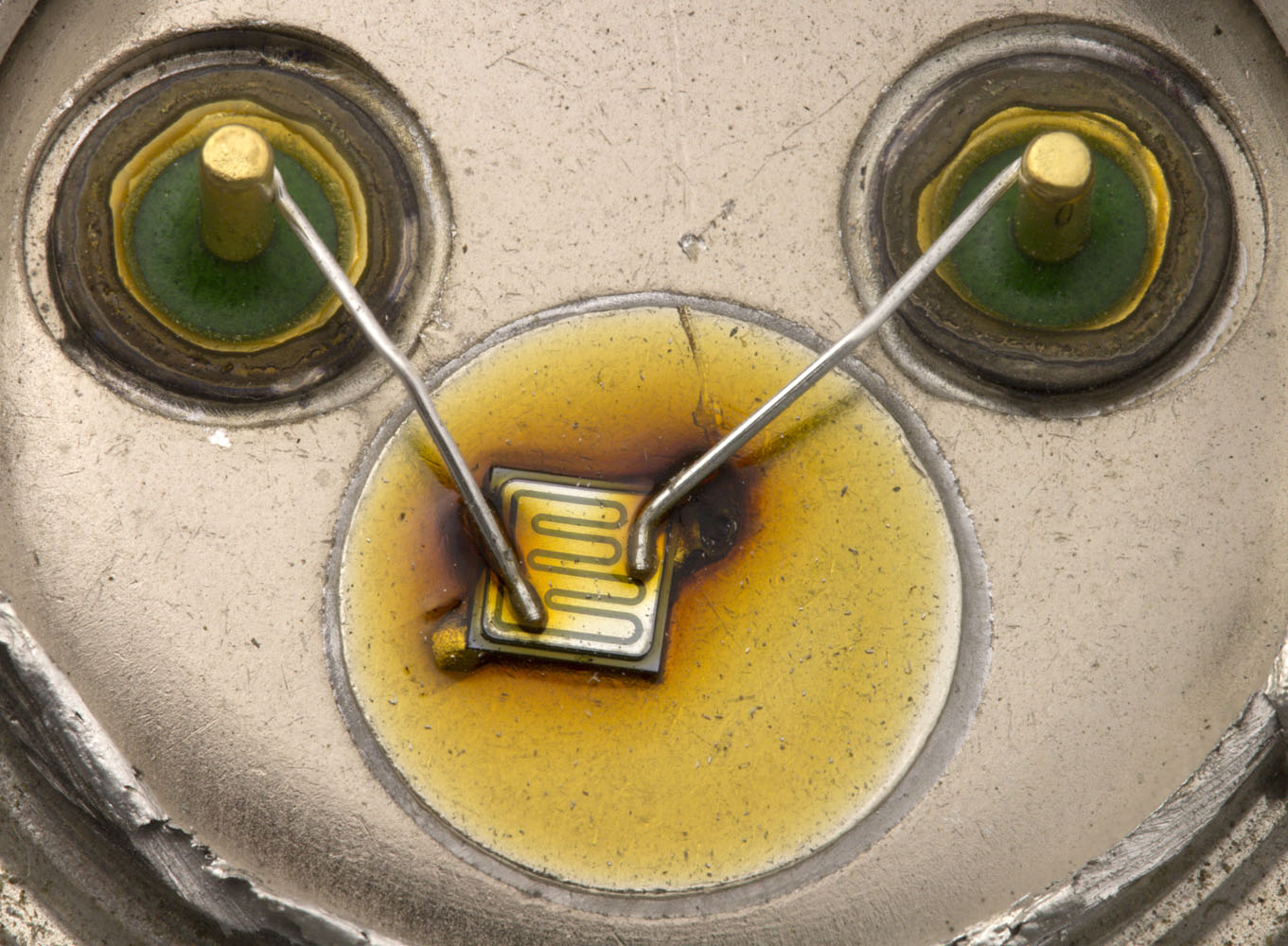
Wow looks beautiful.. must have cost a fortune to assemble/manufacture ! 
If you like to watch pictures of semiconductor dies, then you should check out Richis Lab.
Here is an example from a Motorola 2N3055 transistor. What I really like about those pictures about power transistors is that one can see the barrier layer, because Richi is driving them in reverse mode and then the B-E diode becomes a Zener.

B-E diode working as a Zener at 300mA:

OK just sacrificed a 2N3055 and tried the same experiment. Doesn't work, die doesn't light up. VERY disappointed ! 

Maybe it can't be seen with the naked eye, or it needs a long exposure time to gather sufficient light, or it requires a special version of the 2N3055, I don't know.
All I can say it that it didn't work on my particular transistor, and I now have one less 2N3055, he died for nothing. I am sad now.
I have to correct myself regarding the B-E diode is becoming a Zener. This is only partially true. The main effect is, that the B-E diode is working in avalanche mode. Depending on the materials being used, the produced light can be anything from IR to blue (SiC for example). Richi states, that the light can be visible to the naked eye, but it is mostly very dim. So, if you want to see this effect, it is perhaps a good idea to sit in a dark room for about 10 minutes so your eyes can adapt to the darkness and then try again.
Here is a discussion about the glowing effect of B-E diodes working in avalanche mode:
https://www.eevblog.com/forum/projects/transistors-die-pictures/msg3068740/#msg3068740
Wow, a thread dedicated to the subject, with beautiful pictures at that ! So my little shitty experiment is pointless then !

.. but I did it ANYWAY, because nothing beats doing it YOURSELF, and seeing it with your own eyes !!

So I sacrificed yet another 2N3055 transistor... this time I took my time to hack saw it, exercising as much care as I could in a hope I would not destroy / damage the pins/bonding wires inside

So instead of trying to cut the very top of the cap, instead I cut it at the very bottom, because there is much more clearance with the pins, so less chances that the blade might catch them.
Also I removed the blade from the saw frame, and cut on pull, so I could control the blade better. It was a success, for the first time, 4th attempt, I now have a TO3 that survived its convertible top conversion !

That means I don't need to stick my SMD probes directly onto the die any more, which was hardly reliable and convenient, I experienced...
Now I can just use grabbers to connect to the outside pins, wire that to the power supply, and I have both hands free to play with the controls on the power supply, and hold the camera steady with both hands. It's getting luxurious can't you see ? !

Thanks to this much better controlled testing environment, I was able to achieve success, look at that !!!


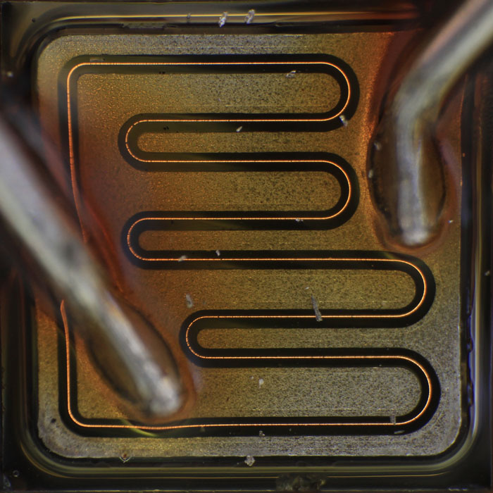
The B-E junction in reverse starts breaking down / conducting at about 15.2 Volts. To get this picture I put 1.2 Amp into it, Voltage rose to 18V or so. I closed the window shutters to make the lab dark. Then opened the shutters half way and noticed the camera could still pick-up the glow, using the highest ISO setting, 6400.
As you can see the glow does not spread across the entirety of the "path" / squiggly line, for some reason I am way too stupid to explain.
Upping the current has zero effect on this " issue " whatsoever. Past one ampere, upping the current does not increase the glow, it stays where it is. Past 2 amps, suddenly the glow disappeared and was reduced to one single tiny dot in a corner of the die. I thought OK I blew it, too much current, had to happen... but then I lowered the current limit on the power supply and the glow came back ! It's still alive and going, this transistor is a warrior !!!

Everyone should have a 2N3055 in his life !

Wow that was a cool and fun experiment ! Everyone should do that !

Think I will archive the pics and my test results/notes on it, it was that cool.
EDIT : The experiment cost me more than a few TO3 pacakges... cost me also one of my Hirschmann long grabbers ! Package got so hot during the experiment that it badly melted the tip of the insulation of the black grabber !!

-group-therapy-thread/?action=dlattach;attach=1496851;image)
-group-therapy-thread/?action=dlattach;attach=1496857;image)