One more analog switch?

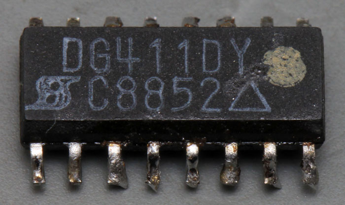
Siliconix DG411 contains four switches SPST-NO. You can buy DG412 with four NC or DG413 with two NO and two NC.
The DG411 can switch up to 40V while supplied with 44V. The resistance of the switch is 35

. Switching time is typically 100ns. Power consumption is less than 35µW.
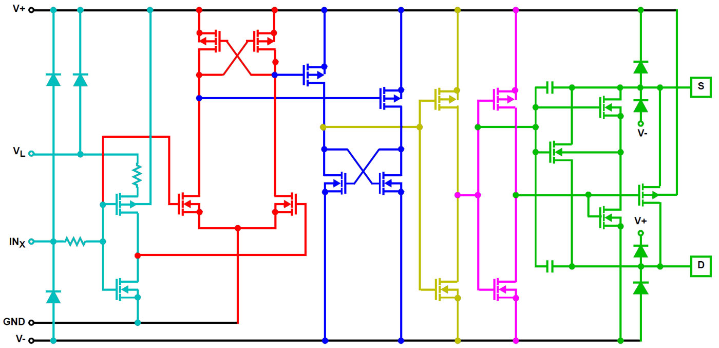
In the datasheet you can find a quite complete schematic. I have colored it.
The input stage can be driven with a different voltage level than the analog switch itself. There is an inverter in the first place (cyan). The input is protected with clamping diodes and a series resistor. There is an additional diode clamping VL against V+. That is important because the substrate is connected to V+. If there is a higher voltage than V+ there is current flow through the substrate.
The inverter generates a differential signal for the first differential amplifier (red). This amplifier converts the high level to V+. The second differential amplifier (blue) converts the low level to V-.
There are two inverters (yellow/pink). The first one probably can be bypassed to switch between a NO and a NC switch. We will talk about the analog switch itself later (green).
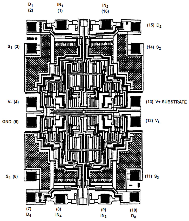
Datasheet contains a pictures of the metal layer. Datasheet states the size with 2760µm x 1780µm x 485µm. There is even a specification of the metal layer. It´s SiAl with a thickness of 1,2µm +/-0,1µm. Adding silicon is important so the aluminium doesn´t migrate into the silicon structures shorting them. Passivation is 0,8µm +/-0,1µm of silicon nitride.
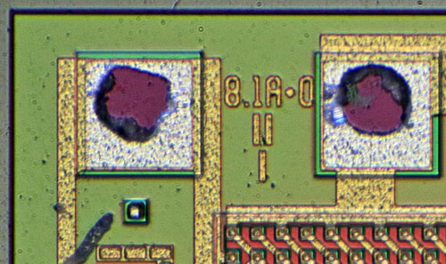
Siliconix

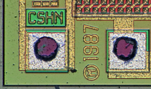
Design is from 1987. CHSN could be initials of the developers.
I assume switching between DG411, DG412 and DG413 was done by changing the metal layer. These characters could be markings for the different variants.
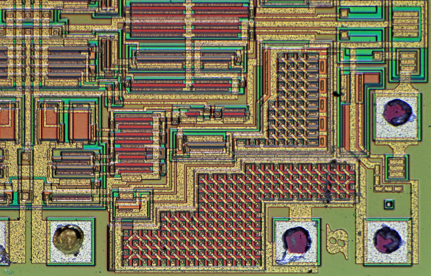
Except for the power supply there are four perfect symmetrical areas containing the four analog switches.
Most of the area is occupied by the two big transistors, the NMOS and the PMOS.
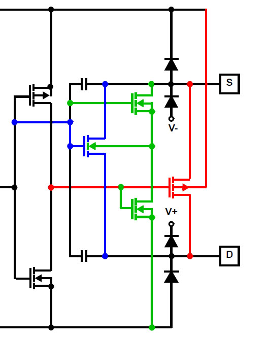
The analog switch itself looks quite complex but it isn´t. You have the NMOS (blue) and the PMOS (red). Bulk of the PMOS is connected to V+. Bulk of the NMOS is switched between the S pin and V- (green) like we have seen in the other analog switches.
We have clamping diodes to protect the structure.
I´m not sure why they have integrated the capacitors.

I assume they stabilize the gate potential against the input signal.
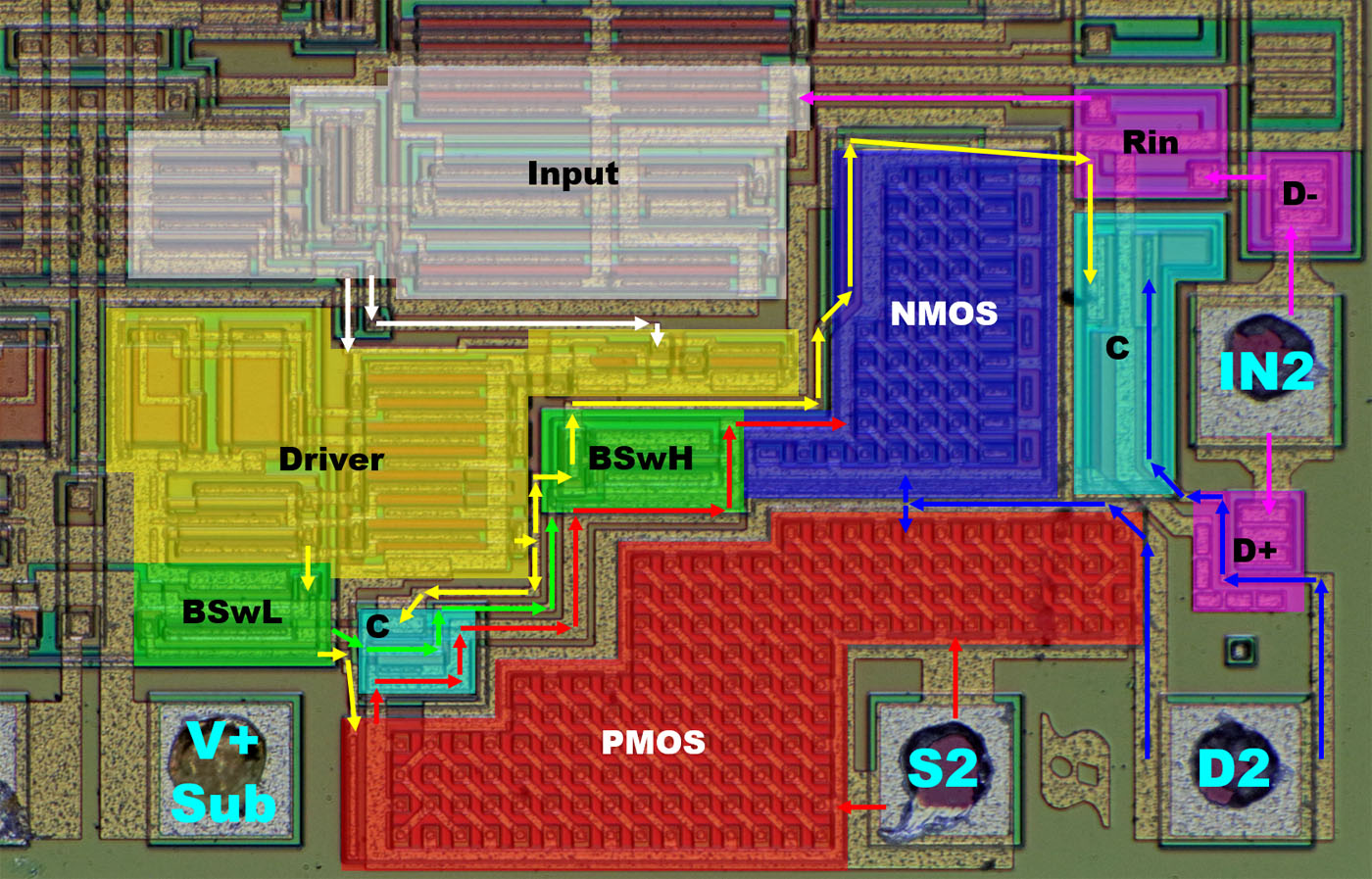
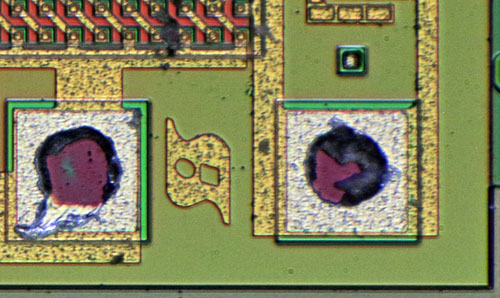
You can find nearly everything we talked about on the die. There are the protection diodes and the series resistor of the control input (pink).
There is the input stage supplied with VL and GND (white) and the rest of the driver stage (yellow) supplied V+ and V-.
You can find the two bulk switches (green) and the capacitos (cyan). One of the capacitors is bigger. That´s probably because on the other side there is one of the bulk MOSFETs increasing the capacitance of this path.
But there is no (clearly visible) protection diode at the input of the analog switch. That´s strange.

Of course it´s possible that these diodes are parasitic elements but I don´t see a straight path to the supply. That´s even more puzzling compared to the accurate input protection of the control input.
https://www.richis-lab.de/aswitch06.htm 


