Hi all!
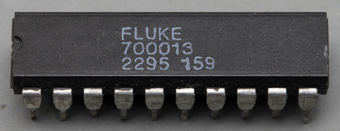
TiN had sent me a 700013 and I have taken some pictures of the die.

Well you know what it does...
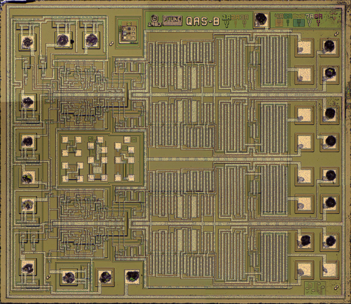
The die is 2,6mm x 2,3mm.
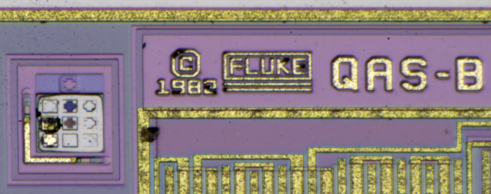
A 1982 Fluke design.
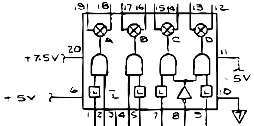
QAS-B seems to be the name of the switch. In the servicemanual of the 8842A the chip is named "IC CMOS, QAS, PLASTIC, HIGH, B Grade". Sounds feasible!

Fluke used eight masks to manufacture the switch.
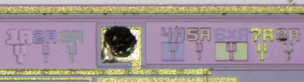
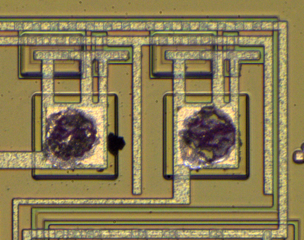
Some test structures.
On the right side there are three different type of the resistors.
On the left side it seems like there are complementary MOS transistors. You can see the small spot in the middle of the cross where the thin gate oxide is placed.
In the middle perhaps some bipolar transistors?
Let the music play!

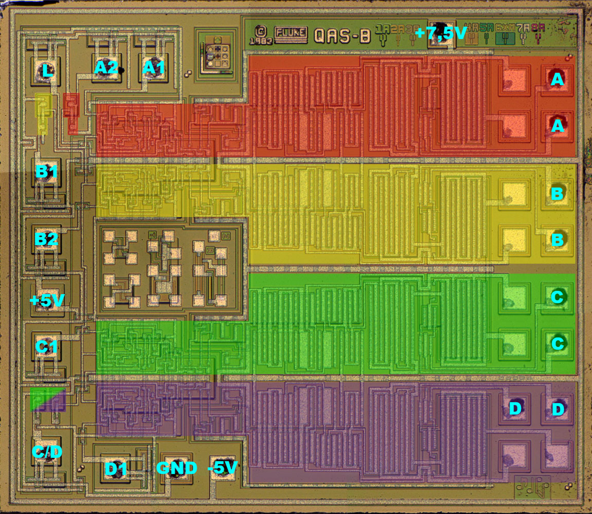
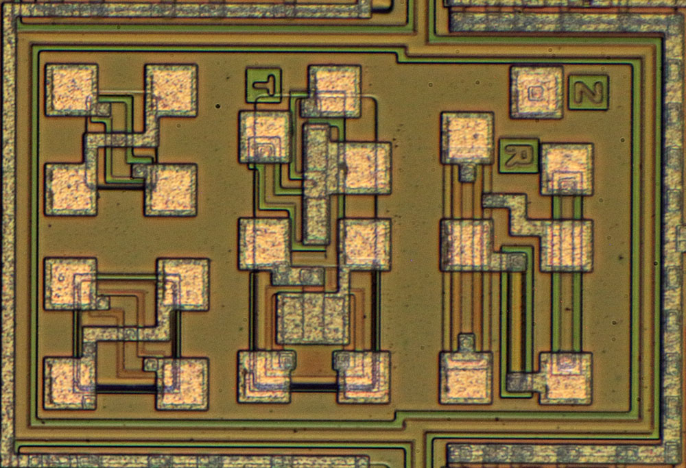
The four switches are easy to spot.
You can see that the left control side is supplied with +5V and 0V while the right switching side is supplied with +7,5V and -5V (of course other voltages are possible).
Some protection at the input pins.
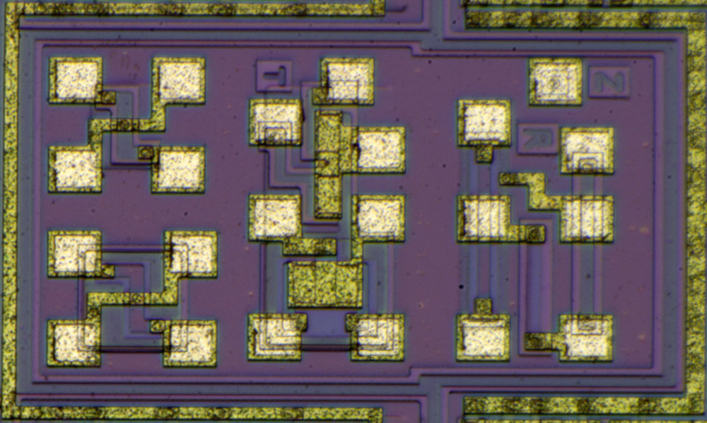
On both sides of the analog switches there are metal lines to isolate the switches. On the left side +5V/0V and on the right side +7,5V/-5V.
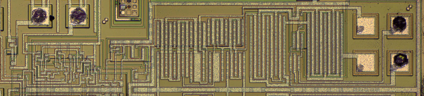
The inputs without the latches are fed into a kind of a push-pull-stage before reaching the control circuit.
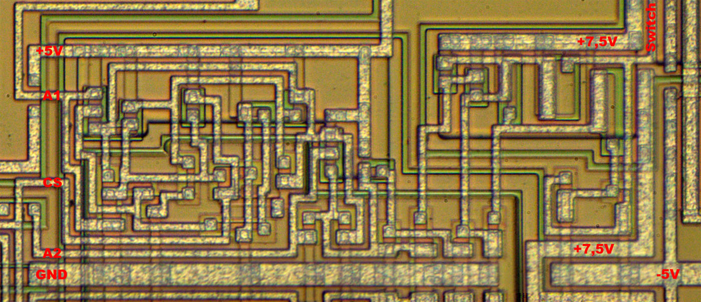
The control circuit contains the latch, the AND gate and the chip select.
The upper area is connected to +5V, the lower area is connected to 0V.
On the right side of the picture there is the transition from +5V/0V to +7,5V/-5V.
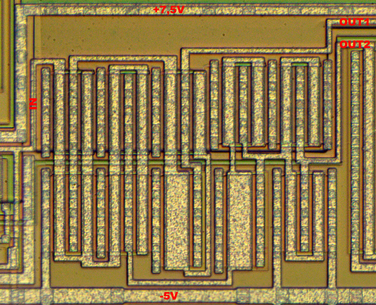
To control the analog switch quite a big differential push-pull-stage was integrated.
It seems like the transistor areas were optimized for ideal switching behaviour.
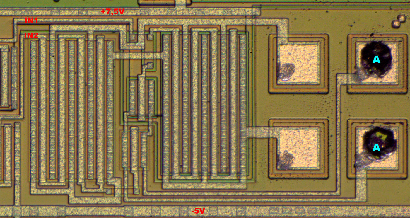
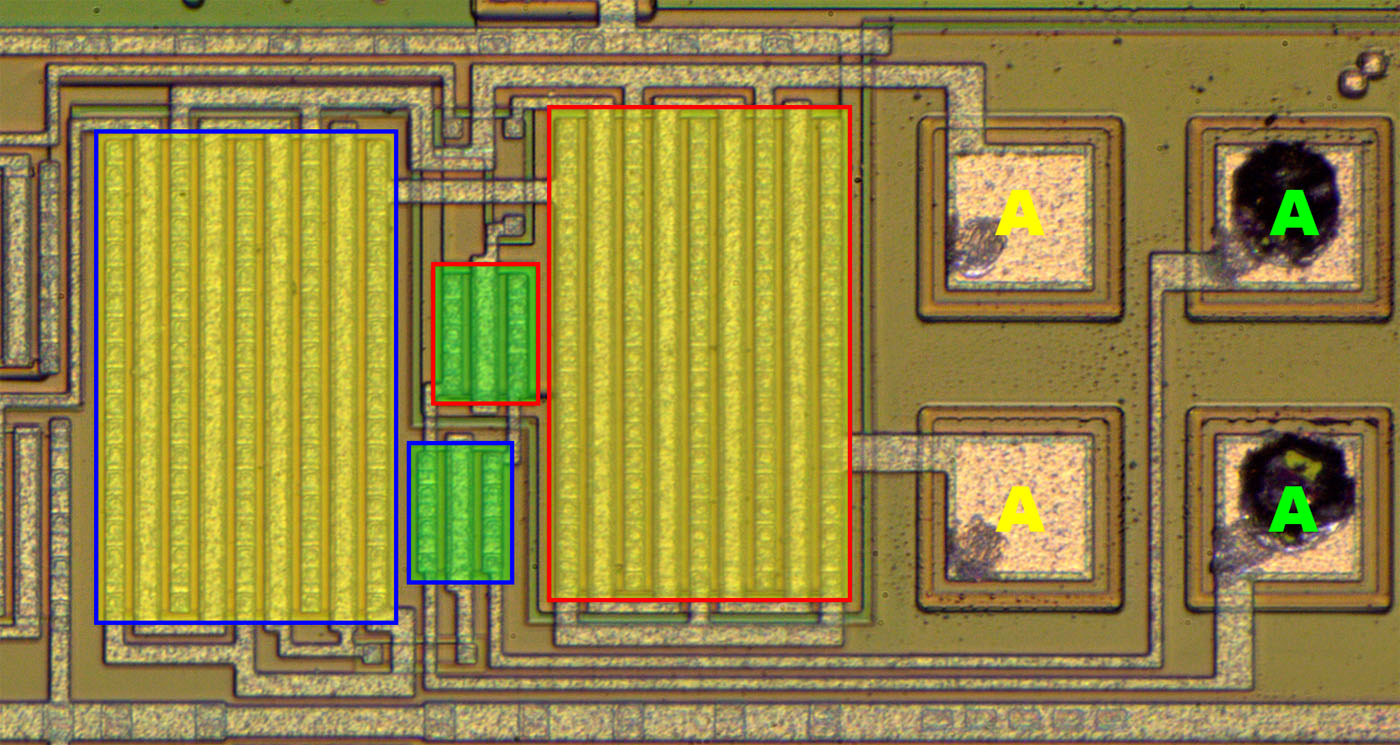
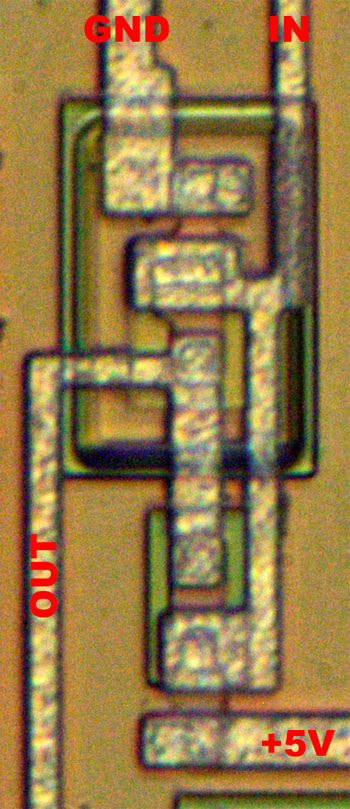
Now that is interesting: There are two small MOSFETs doing the switching of the analog channel. But there are two additional bigger MOSFETs connected to two unused bondpads. It seems like you can choose which transistor you like: a big one with low resistance but with a high leackage current and parasitiv capacitance or a small one with a higher resistance but with lower leackage and capacitance.
https://www.richis-lab.de/aswitch01.htm 


