I was able to get my hands on a USRP2920 thru my university (University of New Haven), and I decided (with prior permission of course) to tear-down the SDR and have a look what's inside, as well as take (what I hope are) decent quality images of the inside.
The picture dump can be found in this Google Drive folder:
https://drive.google.com/drive/folders/16ghueGa5GzQUGbBPaUof810jEpiQ5hHx?usp=sharingI would have written a blog post about it and post-processed the pictures (I have the RAW files), but it is 2am as I am typing this and am too tired to do so.
If you are interested in seeing what is underneath the input PCB where the FPGA lives, let me know. I didn't go that far in this teardown...yet.
Here are a couple of things that I found that are interesting so far, not a complete list and not in any particular order:
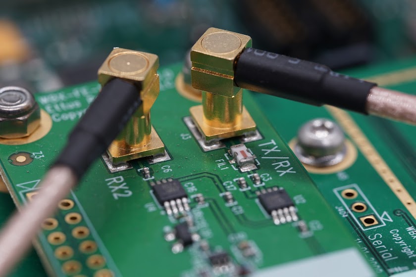
- The RF input is attached to the input PCB with coax instead of a direct-connection. This probably makes sense for the high speed we are dealing with, maybe. Makes it look like a heart

- Some inductor porn

- The TX/RX1 input has a filter in series before the connector, but RX2 doesn't
- One of the jumpers is a genuine marked M3 jumper, which I have never seen before neither did I know that M3 made jumpers


