Author Topic: Looking inside an aerospace DC-DC converter module  (Read 4563 times)

0 Members and 1 Guest are viewing this topic.

Online D StraneyTopic starter

  • Frequent Contributor
  • **
  • Posts: 255
  • Country: us
Looking inside an aerospace DC-DC converter module
« on: December 22, 2023, 03:30:51 am »
Here's an old Interpoint (now part of Crane Electronics) DC-DC module that I got for very cheap recently and opened up, for a look at power conversion in the aerospace world:


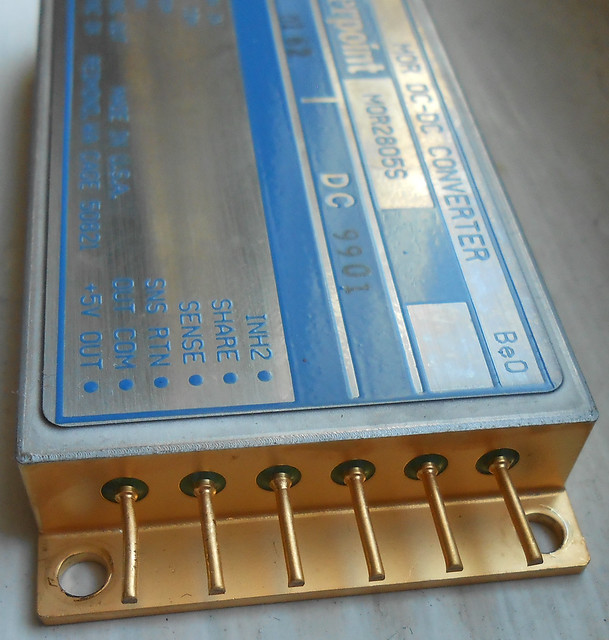
Sealed package with gold plating, hermetic feed-throughs, all the nice expensive stuff.

Once the lid is sawed off, very very carefully to not chip any ceramic substrates considering there's BeO inside, this is the inside:

The blue ceramic block is the control section, while the white ceramic at the top-left holds the input circuitry and the white ceramic at the right holds the output circuitry, with magnetics in the middle.  The input and output ceramic substrates are likely the BeO, as it's used for its high thermal conductivity.

You can see that the input and output are isolated, from the way that the blue control section is split down the middle with a very clear gap.  I'm not sure whether most of the control loop is on the input or output side, but it does have an interesting control-signal-isolation scheme with a small transformer (visible at the right side of the blue section), instead a normal optoisolator.  I hear that optoisolators have a more severe lifetime limit, as the insulating material becomes more and more opaque over time, and the CTR eventually drops unusually low... It's possible this becomes a limiting factor in these type of applications, and that's why they're using a pulse transformer instead.  There's lots of possibilities for sending a control signal through a transformer: you can amplitude- or frequency-modulate an oscillator, or do some PWM with simple square pulses.  Analog Devices makes some digital isolators with tiny on-chip transformers and 100 Mhz+ frequencies.

Here's a closer look at the input...

...and the output...

...and the thin magnet wire from the current transformer (two secondaries, most likely?) that runs to both input- and output-side controls, probably for current-mode feedback on one side and over-current protection on the other side.


The connections to the pins (besides the power input and output) are done with a wide piece of flex circuit that wraps around the front and back, and solders down to the control board in various places:


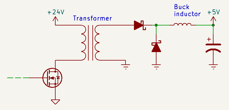
Here's a high-level schematic, along with the corresponding parts:


The output might look a bit weird, but if you re-arrange some components while keeping it functionally equivalent, you end up with a standard forward converter:

Edit: replaced bad flash-heavy photos with better ones
« Last Edit: June 12, 2024, 03:49:54 pm by D Straney »
 
The following users thanked this post: SeanB, TimNJ, radar_macgyver, Neomys Sapiens, schmitt trigger, 5U4GB, Dan123456

Offline Faringdon

  • Super Contributor
  • ***
  • !
  • Posts: 2124
  • Country: gb
Re: Looking inside an aerospace DC-DC converter module
« Reply #1 on: December 22, 2023, 02:04:11 pm »
Thanks, it looks like long life at  hi temperature are the requirements.
I wonder if they used a reset winding  in the 2TF trxformer.
Ayk, Sometimes people just put the control on  the sec side and drive the pri fets with isolated gate drivers.
They put the output inductor in the low side...which gives you 2 transformer switching nodes on the sec side, which  doesnt appear optimal.

Page 26 of this shows how you can easily  use a transformer to do feedback isolation...
https://www.ti.com/lit/ds/symlink/ucc28c50.pdf?ts=1703264959296&ref_url=https%253A%252F%252Fwww.ti.com%252Fproduct%252FUCC28C50

Lots of ceram caps right near the board edge...so hope they are de-panelising with a laser

Pretty sorrowful to see no synchronous rectifiers being used...but then again, there are literally no "good" offTheShelf solutions for synchronous rectifiers for 2TF....i have discussed that before on this forum on multiple postings...i have even provided a solution to the problem, but no one is interested....the West buys all its PSUs from China, so why should they be...no criticism of China, who are simply good upstanding hardworking people. Our western middle men are getting themselves nice and fat...so why should anything be done about it. Makes Western military PSUs worse...but who cares?
« Last Edit: December 22, 2023, 05:33:29 pm by Faringdon »
'Perfection' is the enemy of 'perfectly satisfactory'
 

Online D StraneyTopic starter

  • Frequent Contributor
  • **
  • Posts: 255
  • Country: us
Re: Looking inside an aerospace DC-DC converter module
« Reply #2 on: December 22, 2023, 08:01:53 pm »
I wonder if they used a reset winding  in the 2TF trxformer.
I was wondering about that too, that's the part that really doesn't make sense to me: none I can see, so as drawn it would just dump all the stored magnetization energy into the snubber.

Ayk, Sometimes people just put the control on  the sec side and drive the pri fets with isolated gate drivers.
Yeah there's enough ICs on both sides of the gap that I'm not sure whether it's a matter of sending gate drive pulses, or sending voltage feedback, or even sending a peak-current setpoint I guess if the control loop is split across the gap and it's not just using a dedicated all-in-one SMPS controller.
The "SYNC IN" and "SYNC OUT" pins are connected to the input side, but the "SHARE" pin (presumably for current sharing between multiple units) is connected to the output side...which would only make sense if the voltage control loop was on the output side but the oscillator was on the input side, and the feedback through the signal transformer (like I just speculated about, not expecting it to be true) is the peak current setpoint.

They put the output inductor in the low side...which gives you 2 transformer switching nodes on the sec side, which  doesnt appear optimal.
Was also wondering about the reasoning for that, the only thing I can think of is that maybe it improves the common-mode noise.  There could very easily be a flaw in my reasoning here, but see if this makes sense...
In the standard grounded-secondary configuration, the "bottom" side of the secondary is permanently connected to ground, so the "top" side bounces back and forth between, let's call them, Vpos and Vneg.  That puts a net AC voltage across the distributed inter-winding capacitance and creates a common-mode current which has to be returned through an input-to-output cap (or in this case, through the housing).
If you have this low-side buck inductor though, then one switching state has the "top" of secondary @ +5V, and the other switching state has the "bottom" of secondary @ +5V.  Even though the instantaneous voltage across the winding has flipped, the average voltage on the winding is actually staying in the same place (@ +2.5V), and so I think you'd reduce the common-mode current pushed through the inter-winding capacitance pretty significantly.

What's "2TF", by the way?

Offline Faringdon

  • Super Contributor
  • ***
  • !
  • Posts: 2124
  • Country: gb
Re: Looking inside an aerospace DC-DC converter module
« Reply #3 on: December 22, 2023, 10:19:34 pm »
Thanks, woops i meant 1TF in your schem ("1 transistor forward")
Yes i think your explanation about the CM noise is correct, but that a y cap would be needed anyway...and with a solid ground connected to the transformer secondary, its a much better place for a y  cap...but in your kindly  shown schem, both nodes of sec coil are switching nodes...not good for y cap connection. So yes, if no y cap allowed, then the way kindly shown above is best.
« Last Edit: December 22, 2023, 10:24:04 pm by Faringdon »
'Perfection' is the enemy of 'perfectly satisfactory'
 

Offline David Hess

  • Super Contributor
  • ***
  • Posts: 17232
  • Country: us
  • DavidH
Re: Looking inside an aerospace DC-DC converter module
« Reply #4 on: December 23, 2023, 03:01:45 am »
I have seen a few others which were pretty much the same with no aluminum or tantalum electrolytics, but they did not use a Kapton flexible board for interconnections.

I wonder what they do to maintain stability with such a low ESR on the output capacitor.  Old high reliability stuff used hermetically sealed dry or wet tantalum capacitors so had a free "zero" in their response for stability.  Linear integrated circuit regulators can play some tricks with their output transistor to do the same thing.

Hybrid construction and welded connections are good for reliability.

The white substrates look like alumina.  I thought BeO was a reddish-tan color, but apparently it is colorless or white.
« Last Edit: December 23, 2023, 03:03:23 am by David Hess »
 

Offline Faringdon

  • Super Contributor
  • ***
  • !
  • Posts: 2124
  • Country: gb
Re: Looking inside an aerospace DC-DC converter module
« Reply #5 on: December 23, 2023, 06:35:02 pm »
Ayk, current mode control , with say a type 2 compensator, means you have a power stage with a pole (Load r and output cap c) and a esr zero....so the type 2 gives you 2 poles (one at the origin), and a zero......so you just put the pole and zero at low enough frequency to bring the phase down enough at crossover....no matter  where the esr zero is.

Voltage mode is very different of course, since the output has two zeros. A type 3 compensator gives you two pole and 2 zeros to deal with it though. Problem with voltage mode is you cannot have crossover below 2 or 3 times the output LC resonance frequency. Unless you want crossover below the output LC resonance frequency , in which case your transient response will be horrendously slow.
'Perfection' is the enemy of 'perfectly satisfactory'
 

Offline Njk

  • Frequent Contributor
  • **
  • Posts: 311
  • Country: ru
Re: Looking inside an aerospace DC-DC converter module
« Reply #6 on: December 24, 2023, 10:07:14 pm »
A nice work. BTW in some industries, one design rule was that a soldering joint shall bear no mechanical load. Solder provides only electrical connectivity and it shall not be the mean that holds the component on its place. Not a concern for a small smd parts as the weight is negligible, but those beefy smd caps in the output filter area, they're standing like a high-rises. The green dots can be seen, suggesting the caps are glued to the board before soldering. Perhaps the lying position would show better results during vibration testing. On an aircraft, standing places are only for horses, and for good reason. Besides, there are red flexible cables near the terminals. I'm afraid at certain frequencies, because of resonance, the flexes will start flapping like a birds' wings. Not good. Kapton has good thermal performance but poor wear resistance. Just my notes.
 

Online tszaboo

  • Super Contributor
  • ***
  • Posts: 8035
  • Country: nl
  • Current job: ATEX product design
Re: Looking inside an aerospace DC-DC converter module
« Reply #7 on: December 24, 2023, 11:51:37 pm »
Out of curiosity, how many watts/amps is this rated?
 

Offline berke

  • Frequent Contributor
  • **
  • Posts: 259
  • Country: fr
  • F4WCO
Re: Looking inside an aerospace DC-DC converter module
« Reply #8 on: December 27, 2023, 04:40:20 pm »
Out of curiosity, how many watts/amps is this rated?
100W https://www.craneae.com/sites/default/files/resources/MOR_DC_DC_Converters.pdf

Case operating power: +125°C max at full power!  And probably in vacuum too.
 
The following users thanked this post: tszaboo

Offline GridWork

  • Contributor
  • Posts: 36
  • Country: us
Re: Looking inside an aerospace DC-DC converter module
« Reply #9 on: January 02, 2024, 07:07:11 pm »
My first job was testing/designing these exact type of supplies for a different company. The control is split primary/secondary. The error amp is on the secondary side fed power by the control transformer. The reset voltage of the control transformer carries the control voltage back across the isolation boundary to be decoded on the primary side. This is if I am remembering correctly, it has been a few decades.
 
The following users thanked this post: D Straney

Online D StraneyTopic starter

  • Frequent Contributor
  • **
  • Posts: 255
  • Country: us
Re: Looking inside an aerospace DC-DC converter module
« Reply #10 on: July 11, 2024, 03:06:39 am »
An update: finally got this module under a microscope and had an up-close look.

Here's the gate driver section:


...with the first-stage gate driver IC (Microchip TC4427) - most of the die area is used for the large-surface-area output driver transistors:


...and the second-stage discrete gate driver transistors:


Here's some miscellaneous ICs in the control section.

Judging by label & only 2 connections, this is probably a 2.5V shunt voltage reference:

Judging by logo, labels, and pin count, this is probably an LT119 dual fast comparator, probably used for peak-current control:

Not sure what this one is but "MOT INC" might be for Motorola?
« Last Edit: July 11, 2024, 04:13:37 pm by D Straney »
 
The following users thanked this post: SeanB, pardo-bsso

Offline AnalogTodd

  • Regular Contributor
  • *
  • Posts: 115
  • Country: us
Re: Looking inside an aerospace DC-DC converter module
« Reply #11 on: July 11, 2024, 04:51:14 pm »
An update: finally got this module under a microscope and had an up-close look.

Judging by logo, labels, and pin count, this is probably an LT119 dual fast comparator, probably used for peak-current control:

Not sure what this one is but "MOT INC" might be for Motorola?

Definitely the RH version of the LT119 (minor process tweaks with almost all the same masks to give better RH performance.

As for the MOT INC part, I would hazard a guess that it is a dual op amp given the mirroring between the two sides of the die as it is. Looks like the inputs go together to matched pairs of devices towards the center and all biasing comes from pads on centerline.
Lived in the home of the gurus for many years.
 
The following users thanked this post: SeanB

Online D StraneyTopic starter

  • Frequent Contributor
  • **
  • Posts: 255
  • Country: us
Re: Looking inside an aerospace DC-DC converter module
« Reply #12 on: July 19, 2024, 04:11:02 pm »
Oh good insight, that makes sense.  The lighting isn't good enough to make out the silicon-layer shapes very well, but the transistors in those diff pairs under the metal look circular, which I think makes this a bipolar-input op-amp with PNP inputs? (narrows it down a bit)  Looks like there's a couple interconnected transistors right next to the diff pair which could very plausibly be the "differential-to-single-ended current mirror".  There's also some kind of mystery device in the path of the inputs, before they reach the diff pair, (left-center) which might be some kind of input clamping like anti-parallel diodes?


Share me

Digg  Facebook  SlashDot  Delicious  Technorati  Twitter  Google  Yahoo
Smf