Author Topic: Transistors - die pictures  (Read 221730 times)

0 Members and 2 Guests are viewing this topic.

Online T3sl4co1l

  • Super Contributor
  • ***
  • Posts: 21972
  • Country: us
  • Expert, Analog Electronics, PCB Layout, EMC
    • Seven Transistor Labs
Re: Transistors - die pictures
« Reply #900 on: June 27, 2024, 04:35:20 am »
I think I've seen Vgs(max) by characteristic (zener voltage) rather than rating before, but I can't recall a specific example so it's probably been a while -- uncommon.

They should do fine, being small zeners, but beware the voltage might not be well controlled, the current rating quite small, and the breakdown voltage is usually pretty high besides, and you might not want to idle the gate at 20V or whatever, when all you need is 5 or 10V.

Tim
Seven Transistor Labs, LLC
Electronic design, from concept to prototype.
Bringing a project to life?  Send me a message!
 

Online David Hess

  • Super Contributor
  • ***
  • Posts: 16897
  • Country: us
  • DavidH
Re: Transistors - die pictures
« Reply #901 on: June 27, 2024, 10:20:35 am »
I wondered if it was Control Data Corp? but they didn't use house-labelled that I could find. I got them from a surplus store around 1976, they had bushels and couldn't give them away almost. Some on mainframe looking huge PC boards.
Minimum Cost Semiconductor Silicon Survey (April 1969) of Fairchild TO-105, TO-106 parts. 2N5136 $0.11 "Not recommended", " need not supply a data sheet for publication... none of the readers of 73 would be interested."  :-DD

That is what I was thinking; maybe Fairchild house numbered them for Control Data Corp.

I just checked and the small white CDC ones that I can find immediately are marked CDC CS2923 and CDC CS2924, and also I have these part numbers as 2N in the older "top hat" style TO-92, and probably in real TO-92.  The all black ones seem to all be Fairchild, and some of those are also marked Singapore.  All appear to have date codes through the 1970s.

Somewhere I am sure I have some of the larger packaged white CDC ones.  I might have pulled all of the white CDC ones off of forgotten boards, but many appear new with the original lead lengths.

Here we see a transistor built by Continental Device Corporation similar looking to ours with a "CDC" on the side of the white ceramic:

https://archive.org/details/bitsavers_ElectronicignV15N1419670705_116901282/page/72/mode/2up?q=%22Continental+Device+Corporation%22

That resolves who CDC is, but I notice something else in that advertisement which explains why CDC is not listed in my transistor D.A.T.A BOOK.  That advertisement also shows RTL ICs with the Fairchild part numbers and packaging.  Is there any reason not to think that CDC was simply reselling Fairchild products with a CDC house numbers and markings?

I did not know that the Electronic Design trade magazine went back that far.
« Last Edit: June 27, 2024, 10:24:39 am by David Hess »
 

Offline exe

  • Supporter
  • ****
  • Posts: 2599
  • Country: nl
  • self-educated hobbyist
Re: Transistors - die pictures
« Reply #902 on: June 27, 2024, 02:07:27 pm »
I don't think anyone ever actually put any rating datapoint on them; max shunted current/energy, reverse leakage, etc.

No, and I'd say most transistor parameters are loosely specified. Like, leakages, or threshold voltage.

My expectation is that  VGS(MAX) should be safe to apply for extended time, and built-in zenner should not leak more than maximum leakage current over the whole temperature range. However, I'd also derate gate voltage for two reasons: 1) I don't know if this is harmful or not (some DS have disclaimer that working at maximum specs reduce reliability, but others don't have it) 2) transients etc can make it exceed the specs.

On the other hand, zener should start conducting below dangerous for mosfet voltages, right?) So, if gate current is limited, then it should be safe at all times). But I wouldn't bet on this.
 

Online NoopyTopic starter

  • Super Contributor
  • ***
  • Posts: 1825
  • Country: de
    • Richis-Lab
Re: Transistors - die pictures
« Reply #903 on: June 27, 2024, 07:12:53 pm »
Regarding the protected MOSFETs:
It´s always the same: If it is not specified in the datasheet you can´t be sure.  >:D
Nevertheless I would expect that the abolute maximum rating of Vgs should be possible without relevant leakage current.
For the PMPB19 it´s not a bigger problem. The absolute maximum rating is +/-10V. That is pretty low. I assume the Gate can withstand 15V or even 20V. Between 10V and 20V there is enough room for zener breakdown voltage tolerance and leakage current.
More interesting is something like the STY60NM60 (https://www.st.com/resource/en/datasheet/sty60nm60.pdf): Absolute maximum rating Vgs=30V!  :o
But here the datasheet states that the zener doesn´t break down below 30V and up to this voltage up to 1mA leakage is allowed.


That resolves who CDC is, but I notice something else in that advertisement which explains why CDC is not listed in my transistor D.A.T.A BOOK.  That advertisement also shows RTL ICs with the Fairchild part numbers and packaging.  Is there any reason not to think that CDC was simply reselling Fairchild products with a CDC house numbers and markings?

Well that´s of course possible. Perhaps these transistors are Fairchild parts with a CDC branding.

Offline floobydust

  • Super Contributor
  • ***
  • Posts: 7197
  • Country: ca
Re: Transistors - die pictures
« Reply #904 on: June 27, 2024, 07:44:49 pm »
Transistor reliability was poor back then, Fairchilds known to fail if you tapped them on the side... it must have been interconnects/bonding wires or something.
As well as the die design and fab not performing or competing well. Motorola was giving them a very good run back then. Competition was fierce.
So they would likely have a sales/surplus channel to sell off the poor performers at discount pricing. Perhaps CDC was that.
 
The following users thanked this post: Noopy

Offline SeanB

  • Super Contributor
  • ***
  • Posts: 16344
  • Country: za
Re: Transistors - die pictures
« Reply #905 on: June 27, 2024, 07:56:46 pm »
Found a board with those small white ceramic transistors, with IC's on it (TTL 54 series) that are dated 1977. White ceramic are marked E111, dated 7726, next to a LM218 from National, dated 7809, and an odd transistor from Vactek, partial part number VTL2??? wonder what that 4 leg device is, and looked it up and it is an optocoupler, LED driving a CDS cell, looking like an IR silicon LED.

https://www.datasheetarchive.com/pdf/download/distributors/Datasheets-8/DSA-152236.pdf?h=838accbe3c51ebcbb1e90291f22d175b%3A6eb27fe37141c7c2ba00cc294ac7594ee0%3Ae0393f1b8a637e5dd423f997a5749c5e

Interesting little unknown part. Should see about popping it into an envelope if anybody wants to decap it. The R&S boat anchor it comes from is both a dead item, and was heavy. But really interestng design wise though, and dating from around 1979, though it looks like there were some infant mortality on a lot of IC's, with them having 1984 to 1986 date codes, and not mil spec or industrial range on random ones that likely failed. Looks like the LM1558 IC's all failed in warranty, all changed out with 1980 date codes. Must have had a leaky batch, or they all got purple plague.
 
The following users thanked this post: Noopy

Online NoopyTopic starter

  • Super Contributor
  • ***
  • Posts: 1825
  • Country: de
    • Richis-Lab
Re: Transistors - die pictures
« Reply #906 on: June 28, 2024, 07:52:41 am »
This VTL2 part sounds interesting. I can take a closer look at it if you want me to...  :-/O ;D
 
The following users thanked this post: quince

Offline SeanB

  • Super Contributor
  • ***
  • Posts: 16344
  • Country: za
Re: Transistors - die pictures
« Reply #907 on: June 29, 2024, 11:37:29 am »
Well PM me a postal address and I will drop it into the black hole that is called SA Post office. Might be there possibly Christmas 2025.
 
The following users thanked this post: Noopy

Online NoopyTopic starter

  • Super Contributor
  • ***
  • Posts: 1825
  • Country: de
    • Richis-Lab
Re: Transistors - die pictures
« Reply #908 on: June 29, 2024, 12:18:16 pm »
Done!
I will wait patiently.  :)

Online NoopyTopic starter

  • Super Contributor
  • ***
  • Posts: 1825
  • Country: de
    • Richis-Lab
Re: Transistors - die pictures
« Reply #909 on: July 03, 2024, 12:08:53 pm »


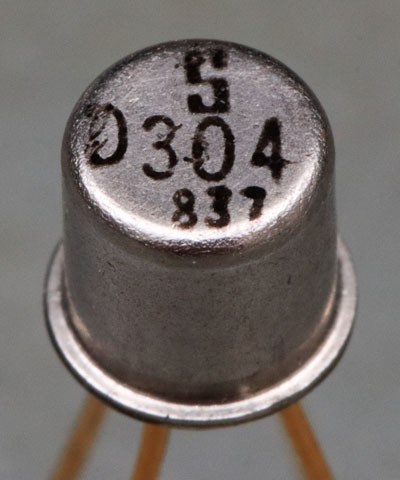
The Signetics SD304 is a dual-gate n-channel MOSFET. It is a DMOS transistor. The gate electrodes are protected against overvoltage by Zener diodes. In addition to the SD304, the datasheet also lists the SD303, the SD301 and the SD300. These are probably different bins. The SD304 can be used at frequencies up to 1GHz. It blocks up to 25V and conducts up to 50mA.


Several scratches and remnants of bondwires can be seen on the bottom of the SD304 package.


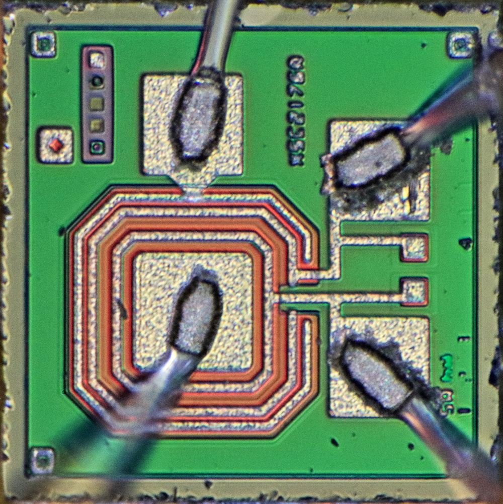
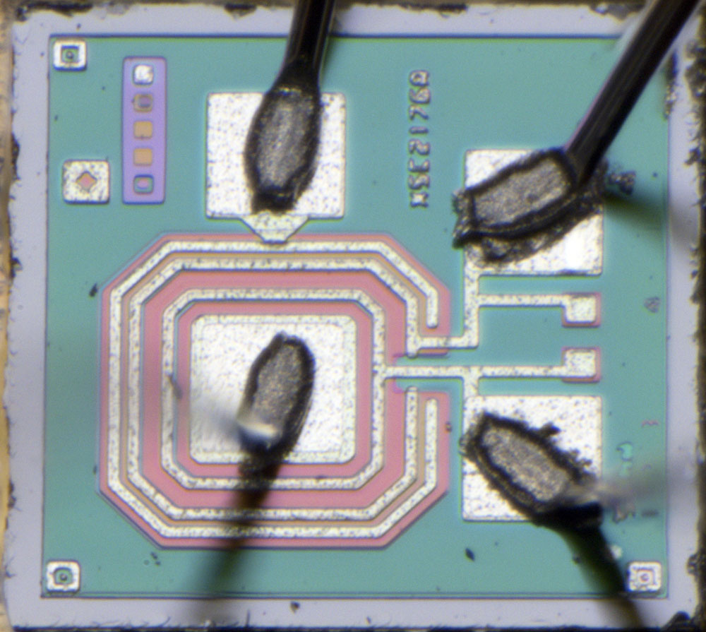
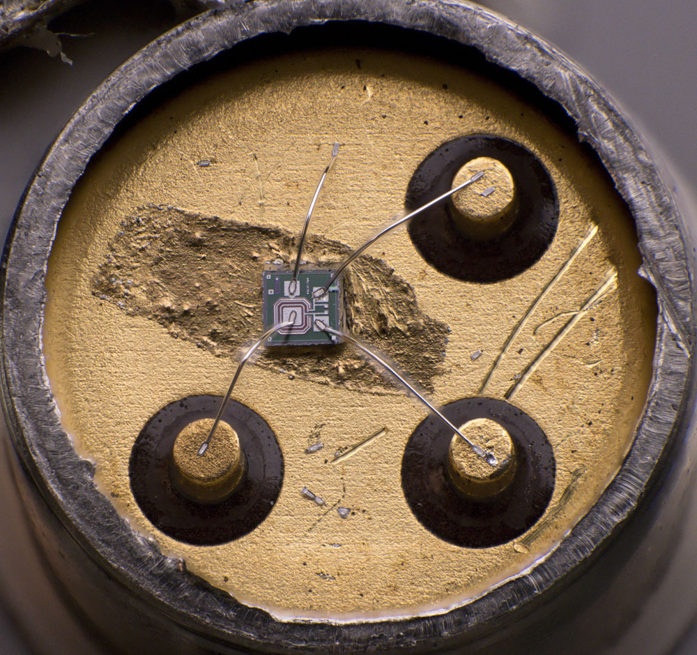
The edge length of the die is 0,50 mm. Square structures in the corners make it easier to place the masks. The auxiliary structure in the top left-hand corner makes it possible to check the alignment of the masks against each other after production. On the right edge, numbers appear to be shown in different levels. However, the characters are so small that the process could not work them out cleanly. There is a string of characters in the upper area. This could be an internal project name.


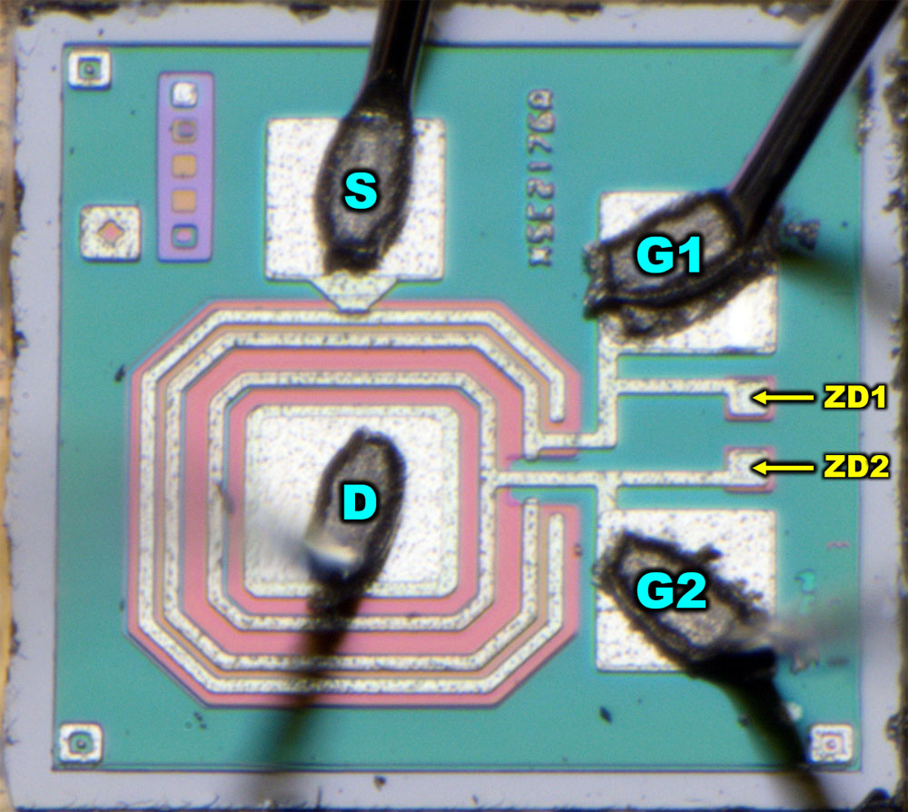
The MOSFET structures are clearly visible. In the center is the drain potential, which is surrounded by two gate electrodes. The outermost ring transmits the source potential. The two protective diodes are integrated at the right-hand edge.

The structures are similar to those in the SM200 (https://www.richis-lab.de/FET45.htm), but here the additional strips that increase the active area are missing. This has a noticeable effect on the transconductance. While 12-24mS are specified for the SM200, the SD304 is specified with just 10mS.


https://www.richis-lab.de/FET48.htm

 :-/O
 
The following users thanked this post: exe, RoGeorge, ch_scr, D Straney

Online NoopyTopic starter

  • Super Contributor
  • ***
  • Posts: 1825
  • Country: de
    • Richis-Lab
Re: Transistors - die pictures
« Reply #910 on: July 06, 2024, 06:56:49 pm »


Like the SD304, the Signetics SD305 is a DMOS transistor with two gate electrodes. It is specified for applications in the range of 200MHz. It is therefore somewhat slower than the SD304. The maximum reverse voltage is 20V. The drain current may increase up to 150mA. In addition to the SD305, the datasheet also lists the SD306. The specifications of the components show that they are not just different bins. The SD306 has a lower current carrying capacity, lower parasitic capacitance, a lower transconductance and a higher channel resistance. Everything indicates that the SD306 contains a significantly smaller transistor.


The source potential of the MOSFET is connected to the package via two bondwires.


The cross-shaped structure of the MOSFET offers a significantly larger active area than in the SD304. This explains the higher current carrying capacity and the higher transconductance, but also the higher parasitic capacitances. The auxiliary structures in the corners and at the upper edge are the same as those found in the SD304.


The slightly thicker metal strip on the right-hand source bondpad does not appear to have any electrical function. It could be an auxiliary structure that facilitates the correct alignment of the die. The Zener diodes, which protect the gates against overvoltage, are integrated near the bondpads.


https://www.richis-lab.de/FET49.htm

 :-/O
 
The following users thanked this post: RoGeorge, D Straney


Share me

Digg  Facebook  SlashDot  Delicious  Technorati  Twitter  Google  Yahoo
Smf