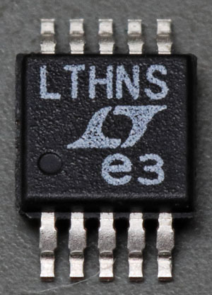
The Linear Technology LT3750 is a switching regulator in an MSOP package. The device is specialized to charge a capacitor to a high voltage. The datasheet lists warning lights, photo flashes, security systems, high voltage sources, electric fences and igniters as possible applications.
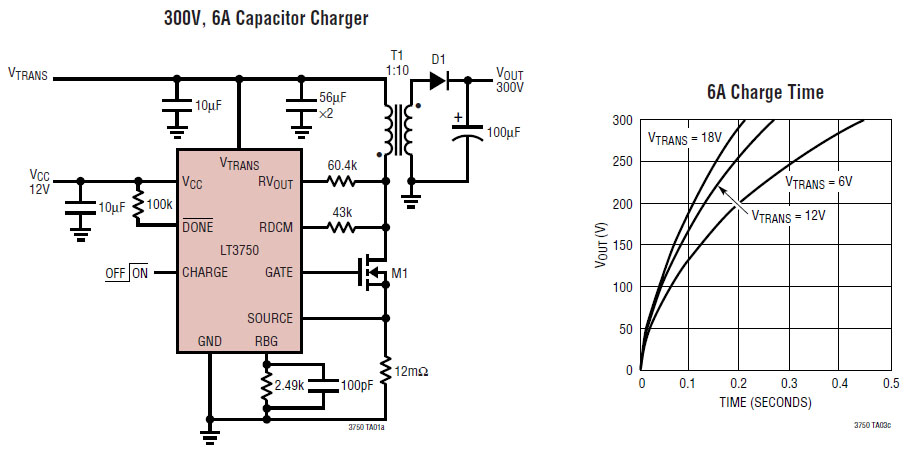
An application example in the datasheet charges a 100µF capacitor to 300V in half a second. It is basically just a flyback converter with a primary side measurement of the secondary voltage. However, the regulator is optimized to charge a capacitor. The datasheet refers to patents 6518733 and 6636021 but these do not describe exactly how the LT3750 works.
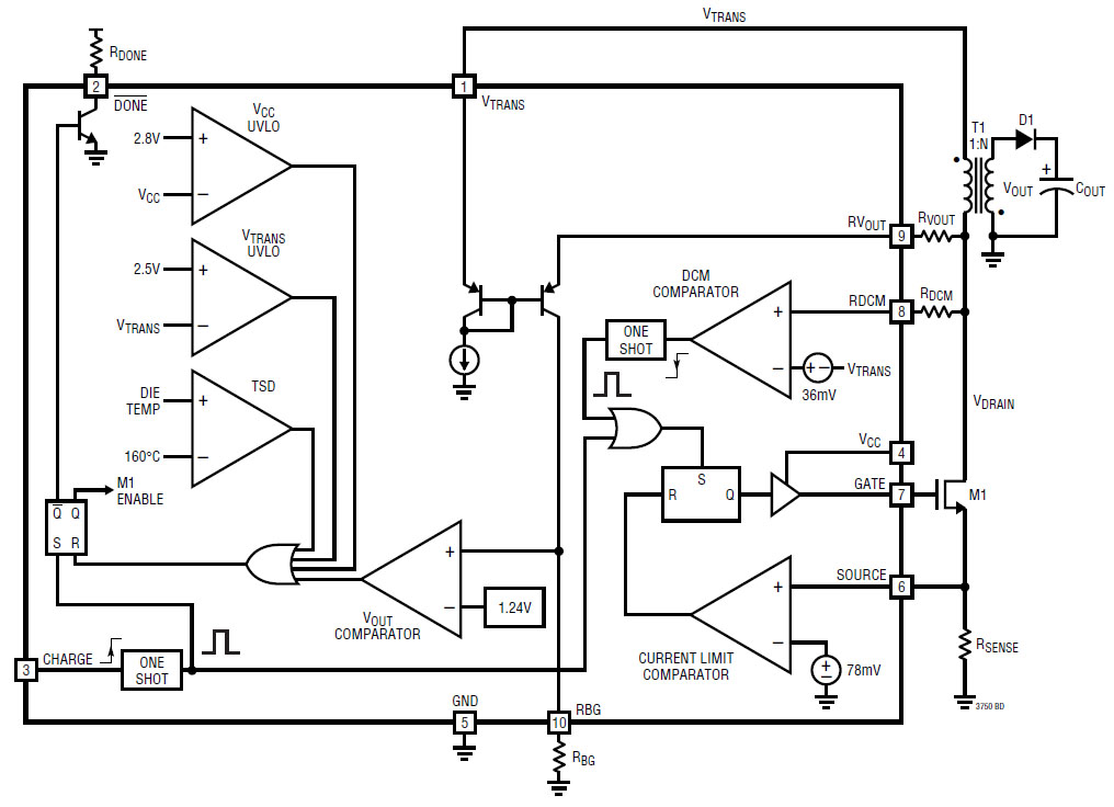
The block diagram in the datasheet shows the operation of the controller. Pulling pin 3 high generates a pulse which enables the control of the power transistor M1 via the left flip-flop and switches the power transistor on at the same time via the right flip-flop. As a result the current through the transformer increases linearly to the limit set by the resistor Rsense. The current limit comparator then ensures that the power transistor is switched off again via the right flip-flop.
The energy stored in the transformer as a magnetic field charges the capacitor Cout via the diode D1 in the blocking phase. In this phase the voltage of the secondary is transferred to the primary in proportion to the turns ratio. When the current flow ends the voltage at the power transistor drops again to the supply voltage Vtrans, whereupon the DCM comparator again activates the right flip-flop and thus the power transistor. The switching frequency ranges between 100kHz and 300kHz.
The secondary voltage transformed to the primary side is monitored via pin RVout. For this purpose the resistor RVout generates with the internal current mirror a current proportional to the transformed voltage. The current mirror is not used in this circuit to simply duplicate a current. It ensures that resistor RVout operates with Vtrans as the reference potential. Thus, the current through resistor RVout becomes independent of the supply voltage of the primary side and is only proportional to the transformed secondary voltage. Equally advantageous the potential at the upper contact of resistor Rbg is independent of the potentials at Vtrans and RVout. The voltage drop across Rbg, proportional to the secondary voltage, switches the Vout comparator when the desired secondary voltage is reached. As a result, the left flip-flop is reset and the Done output signals that charging is complete.
Three other comparators serve as protection circuits and can abort the charging process. Abort occurs when the temperature exceeds 160°C and when the supply voltages drop below 2,5V and 2,8V respectively. The usefulness of the Vcc lower limit is questionable, since the output voltage of the gate driver can already drop to 3V at a supply voltage of 5V. Unfavorably, the Done output is also activated in the error state, suggesting that the charging process was successful.

The primary side measurement of the secondary voltage is particularly advantageous here because a voltage divider on the secondary side would discharge the capacitor. However, many flyback regulators are capable of this primary-side measurement. The LT3750 has the additional advantage that it is optimized for charging an empty capacitor once. It does not need to regulate the secondary voltage, but permanently transfers the same energy packets and deactivates when the desired voltage is reached. This process can be better optimized for minimum charging time than an ordinary regulation. Switching off the regulator may cause a drop in the secondary voltage but this avoids a prolonged dwell in inefficient operating points.
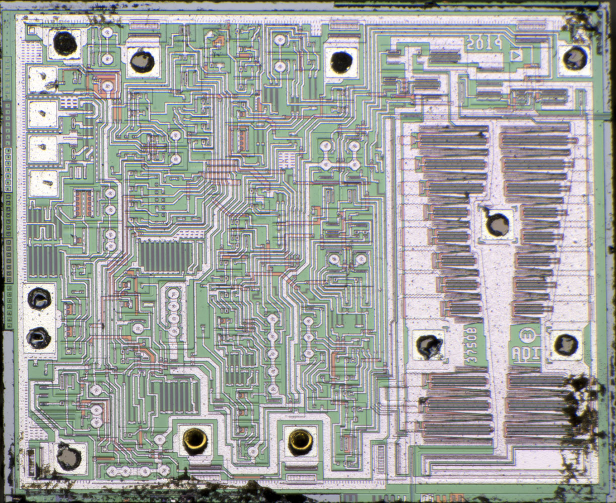
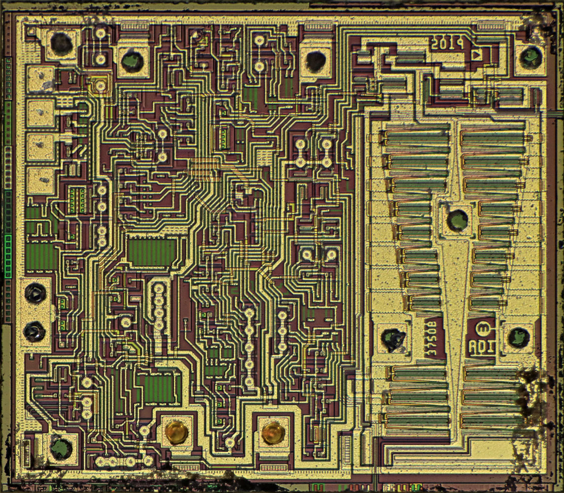
The die is 1,6mm x 1,4mm in size. The large transistors of the driver stage are clearly visible in the right area. The remaining elements are also still quite clear. It would be quite possible to analyze the circuit completely.
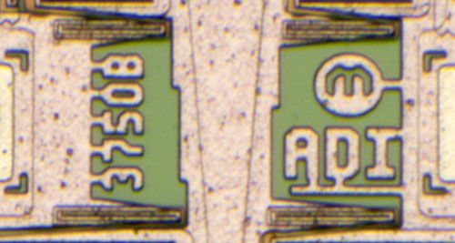
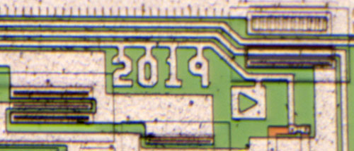
The LT3750 was developed by Linear Technology. However the abbreviation ADI shows that the design has been revised by Analog Devices in the meantime. The B at the end of the designation 3750B probably stands for a second revision.

On the edge there are some patterns that allow to check the alignment of the masks against each other.
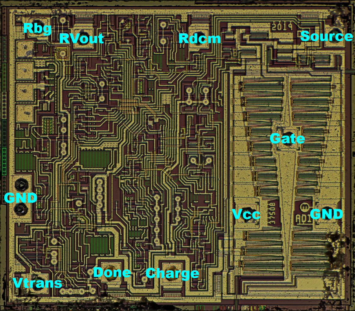
The bondpads can be assigned to the pins of the module relatively unproblematic. The ground potential contacts the device twice, once in the control area and once at the driver transistors.
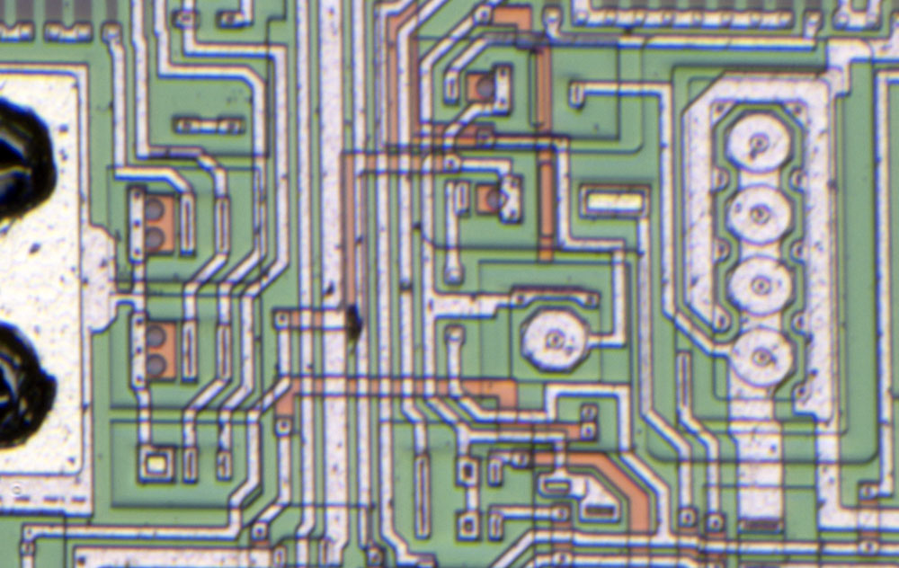
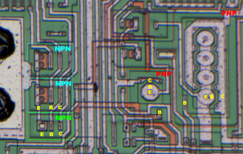
The PNP transistors (red) of the integrated circuit have the usual round structures, where the emitters are located inside. Around the emitter the collector is integrated. Both are separated by a base ring, which is contacted slightly outside.
There are also the usual NPN transistors (green). One thinks to be able to recognize the outlines of a buried collector supply line. The base area is also not visible in color, but can be guessed by the contours, just like the emitter.
Besides the usual NPN transistors there are other, very strange NPN transistors (cyan). Their emitter consists of an orange area with one or more dark circles. The contacting of the emitter apparently takes place in the orange area. Since the orange material is also used as a conductor it must be highly doped. It seems most likely that the orange material is heavily n-doped and the dark circles are even slightly more heavily n-doped. It may also be that they are just dimples. It could be that this generates a low-lying base-emitter interface, similar to a buried Zener diode.

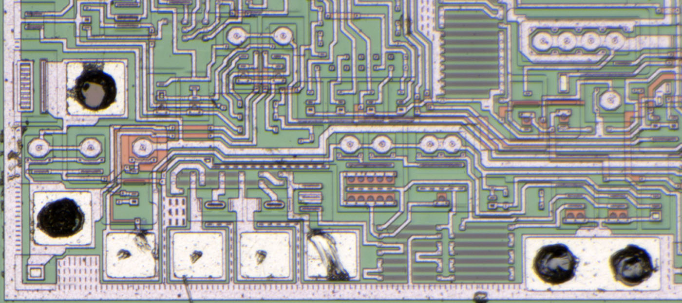
In the upper left area of the die (here rotated by 90°) are four testpads. The many resistors to the right of the testpads and the two very differently sized transistors above them are reminiscent of a bandgap reference voltage source. However, if you analyze the circuitry, you can see that the current sink of the current mirror is located in this area. The current mirror itself is built with three PNP transistors, which are located on the left between the bond pads Rbg and RVout. The current value in the reference path of the current mirror should not be too critical. However, the current sink also determines the switching threshold of the Vout comparator and this threshold should be hit reasonably accurately for all devices, for which an adjustment makes absolute sense.
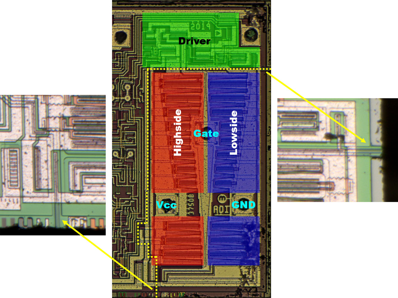
The gate driver consists of a highside and a lowside transistor (red/blue). Above this are the drivers for this push-pull stage (green). The gate driver area is isolated from the rest of the circuit (yellow), which presumably is done to reduce interfering feedback.
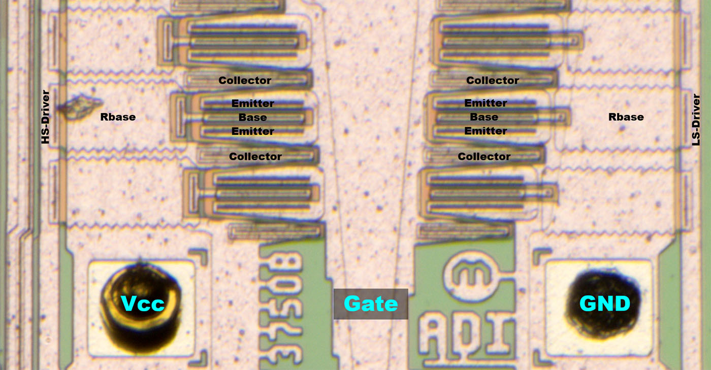
The details show that the output stage transistors have an unusual structure. Both Lowside and Highside contain NPN transistors. However, the base terminal is located in the center and is surrounded by two emitter contacts. The emitter is shaped like a ring.
Also unusual is the large area resistor. One would expect emitter resistors, which provide an even current distribution. However, the resistors are located at the base connections. The current distribution could be influenced in this way, but only as long as the transistors are not operated in saturation, which is certainly the case here. In addition, the control of the emitter current via the base resistors would be subject to very large fluctuations. As will be shown in a moment, there is even more to be said for the fact that these are not measures for uniform current distribution. This means that the individual transistors are constructed in such a way that the current is distributed sufficiently evenly even without balancing resistors.
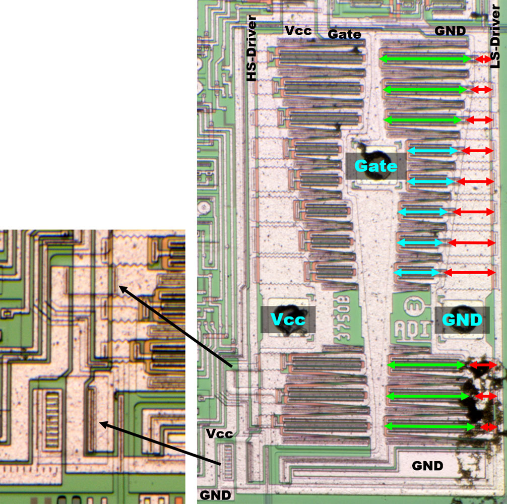
The lines of the potentials Vcc, Gate and GND are designed in such a way that they become wider according to the increasing current load. At first glance, one gets the impression that different transistor sizes have been deliberately integrated here (green/cyan), but in fact one has merely filled in the areas that resulted between the necessary trace widths.
In this context no meaningful correlation between the length of the base resistor and the remaining conditions can be seen. In combination with the very wide design and the use of heavily doped areas, it can be assumed that the strips merely serve as an undercrossing of the metal layer and that their resistance is more of a parasitic property.
The ground potential is connected to the base of the gate driver at the bottom right. It also represents a kind of screen at the left edge. The Vcc potential is led out to the left in the lower area and used to power the rest of the circuit. At the lower edge an element connects Vcc and GND. This could be a Z-diode that dissipates overvoltages. The highside and lowside transistors are controlled from above.
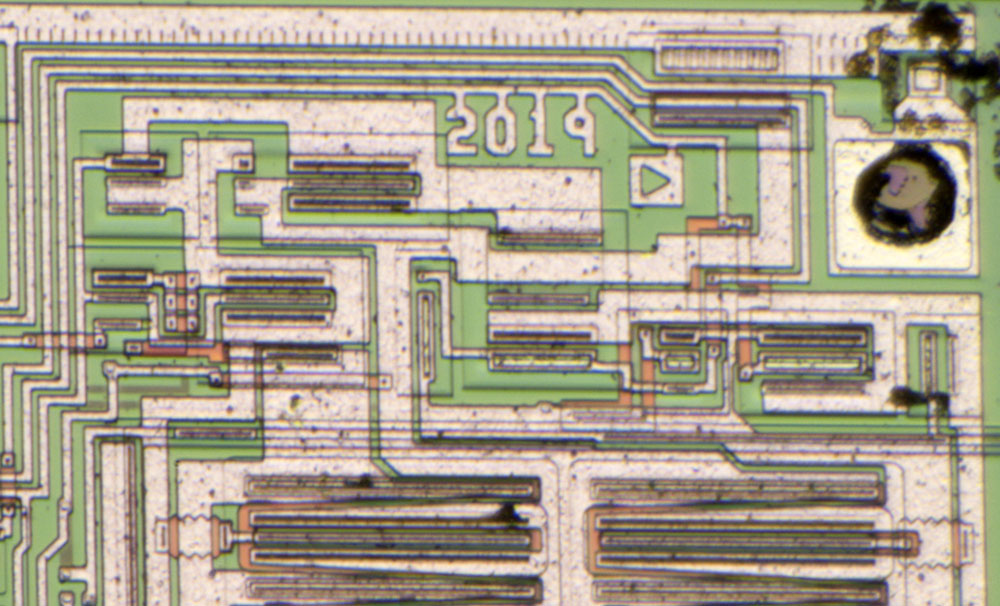
The circuit for controlling the gate driver is located on the upper edge of the die.
https://www.richis-lab.de/voltageregulator18.htm 