Hi all!
Today I have a LM300 for you:
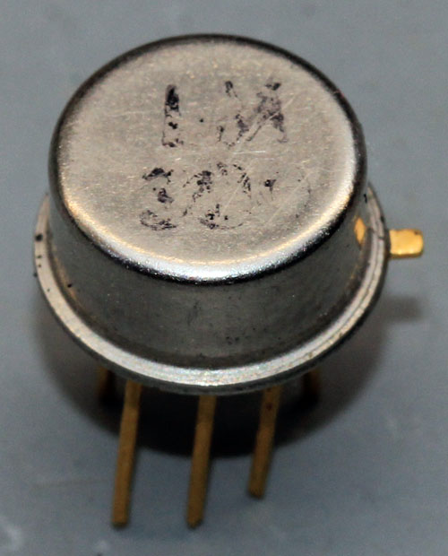
You can barely read LM300.
A nice old design.
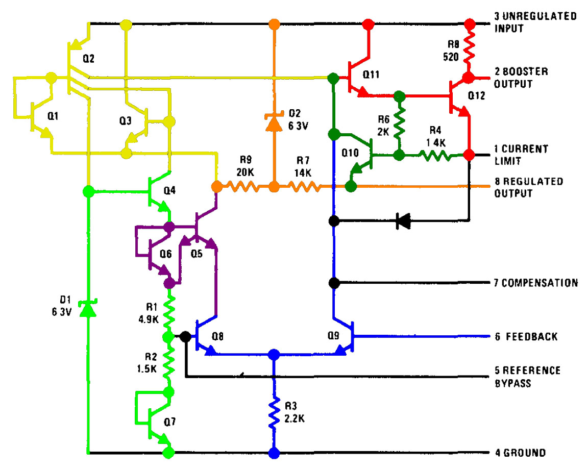
The bright green circuit generates the voltage reference. The reference is based on the zener D1 which causes a constant current through Q4, Q6/Q5, R1, R2 and Q7. At the base of Q8 the voltage is 1,7V.
The transistors Q6/Q5 look like a current mirror but the current in the left emitter of Q5 is also flowing into the reference path.
The current through the left path of the differential amplifier and the current mirrored from the reference path are flowing through the collector of Q5 and are controlling the transistor Q2. Q2 is supplying the regulator. Low output voltages and high voltage drops increase the supply currents. The zener D2 limits the effect of the voltage drop. Probably that stabilizes the bias point.
The red part is the regulator if you short Pin 3 and Pin 2. Without the short you can also use the Transistor Q12 as a driver for an external power transistor.
The dark green part is the overcurrent protection.
The unnamed diode seems to protect the regulator from high voltages at the output.
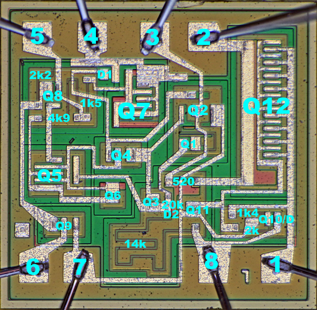
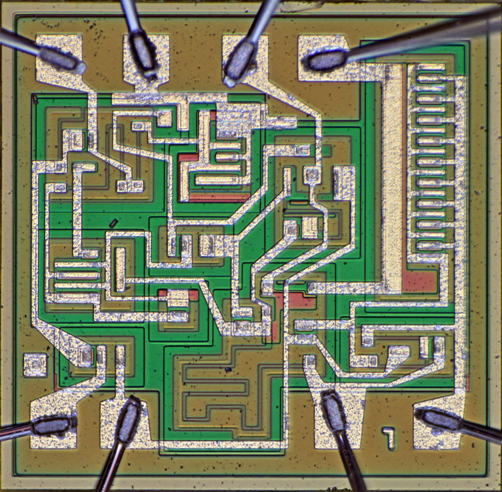
You can find every part of the schematic on the die.
Some of them are quite interesting to identify:
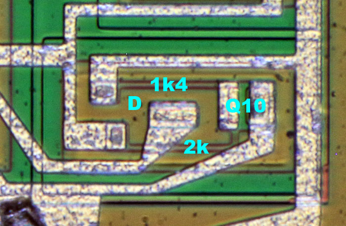
The unnamed diode is a parasitic part in the collector area of Q10 created by the 1,4k resistor.
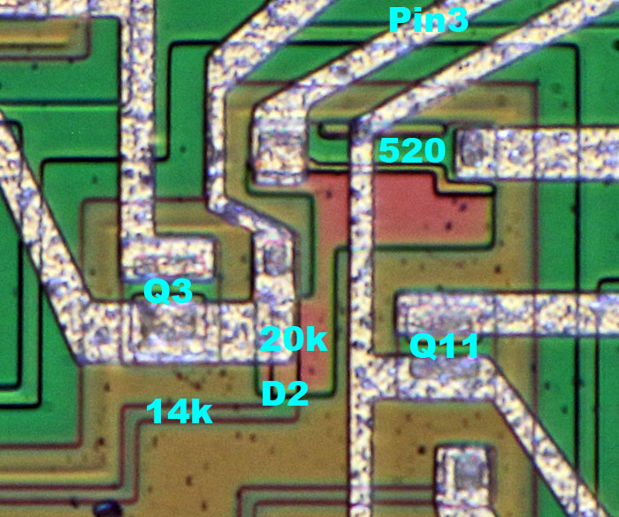
Why is the 520-resistor not connected directly to the Pin 3 metal contact?

The 20k-resistor is quite small but has an n-type overlay. The junction gives us the zener D2.
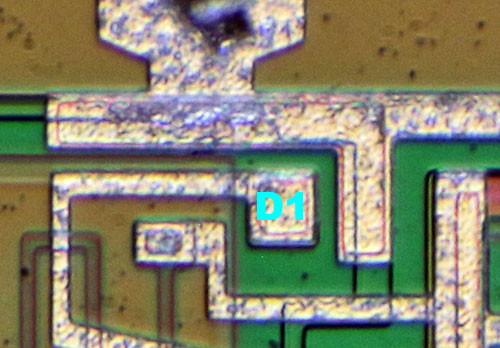
The zener D1 is located near the ground connection in a p-type area.
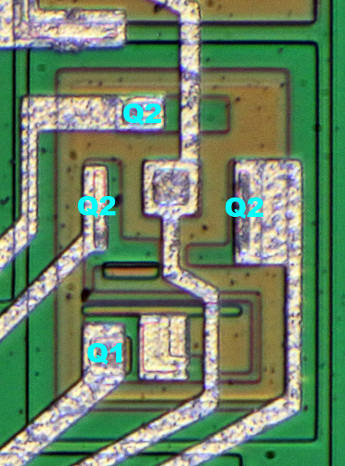
Between the left collector of the pnp Q2 and the base of the npn Q1 there is a small resistor (=high value) which we can´t find in the schematic. Probably the resistor supports start-up.
https://www.richis-lab.de/voltageregulator04.htm 


