Author Topic: Transistors - die pictures  (Read 257122 times)

0 Members and 2 Guests are viewing this topic.

Offline NoopyTopic starter

  • Super Contributor
  • ***
  • Posts: 1895
  • Country: de
    • Richis-Lab
Re: Transistors - die pictures
« Reply #200 on: September 07, 2020, 05:47:22 pm »

I have taken pictures of a Motorola 2N3055I:


It seems like the Motorola 2N3055I has a bigger die than the Motorola 2N3055 (https://www.richis-lab.de/2N3055_07.htm). Perhaps the 2N3055I was a more robust version. Perhaps it´s a different generation of the 2N3055.  :-//
I didn´t find a 2N3055I in the Motorola data books, only a 2N3055A which seems to indicate parts with less ft).  :-//


https://www.richis-lab.de/2N3055_10.htm


 :-/O
 
The following users thanked this post: daqq

Offline NoopyTopic starter

  • Super Contributor
  • ***
  • Posts: 1895
  • Country: de
    • Richis-Lab
Re: Transistors - die pictures
« Reply #201 on: September 09, 2020, 09:10:47 pm »
Hi all!

More power: Darlington-Halfbridge-Powermodul Powerex KD324510  8)


Ugly silicone potting...  :palm:


After a lot of cleaning...


The die is 16,0mm x 12,0mm. Two of them act as highside and two of them act as lowside.


Guard rings for the high voltage.


The diodes are 5,9mm x 3,9mm.
Constant current: 50A
Peak current: 500A


The diodes are also equipped with guard rings.


https://www.richis-lab.de/Bipolar19.htm

 :-/O
 
The following users thanked this post: Miyuki

Offline T3sl4co1l

  • Super Contributor
  • ***
  • Posts: 22436
  • Country: us
  • Expert, Analog Electronics, PCB Layout, EMC
    • Seven Transistor Labs
Re: Transistors - die pictures
« Reply #202 on: September 10, 2020, 12:14:49 am »
Hm, I wonder what the tradeoff is for metallized guard rings versus not.

Tim
Seven Transistor Labs, LLC
Electronic design, from concept to prototype.
Bringing a project to life?  Send me a message!
 

Offline NoopyTopic starter

  • Super Contributor
  • ***
  • Posts: 1895
  • Country: de
    • Richis-Lab
Re: Transistors - die pictures
« Reply #203 on: September 10, 2020, 05:51:48 am »
Perhaps that´s necessary because of surface charge effects?  :-//

Offline NoopyTopic starter

  • Super Contributor
  • ***
  • Posts: 1895
  • Country: de
    • Richis-Lab
Re: Transistors - die pictures
« Reply #204 on: September 10, 2020, 08:15:31 pm »
Today I have a 2N1613 for you:
https://www.richis-lab.de/Bipolar20.htm

The 2N1613 is the first planar transistor worldwide and it´s still produced today.  :clap:


This 2N1613 was built by Telefunken.


A small die (0,7mm x 0,7mm), nothing special...

 :-/O


Now you can find me on patreon: https://www.patreon.com/richis_lab
Do you like my pictures?  ;)
 
The following users thanked this post: RoGeorge, serg-el

Online RoGeorge

  • Super Contributor
  • ***
  • Posts: 6775
  • Country: ro
Re: Transistors - die pictures
« Reply #205 on: September 11, 2020, 07:06:13 am »
Is all the yellow inside a gold plating?  It might justify outside, so the terminals won't oxidize, but why would gold plating be used inside the transistor's case?

Offline NoopyTopic starter

  • Super Contributor
  • ***
  • Posts: 1895
  • Country: de
    • Richis-Lab
Re: Transistors - die pictures
« Reply #206 on: September 11, 2020, 07:22:13 am »
I assume that´s all gold plating.
I further assume that they used gold platingt to assure a good bonding even if the package is stored open some time before attaching the die and closing the package.

Offline T3sl4co1l

  • Super Contributor
  • ***
  • Posts: 22436
  • Country: us
  • Expert, Analog Electronics, PCB Layout, EMC
    • Seven Transistor Labs
Re: Transistors - die pictures
« Reply #207 on: September 11, 2020, 04:29:28 pm »
Might be a combination of bonding and contamination.  If it's bare metal, it's likely to spatter when spot-welded together.  Gold, copper, silver and alloys would be fine as a filler, spot-brazing it as it were.  Maybe just convenience as to putting it everywhere?

If the layer is very thin (as gold tends to be these days), it might not be enough to act as a filler; it might diffuse into the base metal, leaving little or no advantage for bonding purposes.  (It might simply be that a clean and smooth enough interface, with a well controlled welding process, doesn't spatter.  I'm sure this is relevant to later production; I have more than a few TO-39s that are full tin plated, so either would've been bonded like that, or bare and plated afterwards.  Hmm, and at that, most of them are smooth but a few Philips 2N4033 are starting to whisker..!)  If it was a heavier layer of gold, it could serve this way though.

It's interesting that only the base seems to be gold plated, which doesn't really go along great with either theory. :-DD

Tim
Seven Transistor Labs, LLC
Electronic design, from concept to prototype.
Bringing a project to life?  Send me a message!
 

Offline NoopyTopic starter

  • Super Contributor
  • ***
  • Posts: 1895
  • Country: de
    • Richis-Lab
Re: Transistors - die pictures
« Reply #208 on: September 15, 2020, 03:22:11 am »
I have forgotten to post the ITT 2N3055 here:

https://www.richis-lab.de/2N3055_11.htm


The hometaxial structure is easy to see.  :-+


Of course it´s glowing!  8) And the ITT 2N3055 has a high BE breakdown voltage (-18V) as it is typically for hometaxial transistors.


The current density is not perfectly uniform because of a lack of solder.

 :-/O

Online RoGeorge

  • Super Contributor
  • ***
  • Posts: 6775
  • Country: ro
Re: Transistors - die pictures
« Reply #209 on: September 15, 2020, 06:43:34 am »
Looks like the die of the ITT/2N3055 is not flat!   :o
Is that an optical illusion?  Is it even possible to make undulated chips?

Offline NoopyTopic starter

  • Super Contributor
  • ***
  • Posts: 1895
  • Country: de
    • Richis-Lab
Re: Transistors - die pictures
« Reply #210 on: September 15, 2020, 06:51:31 am »
That´s the hometaxial structure.

Where you want to contact the base you have to etch away the emitter diffusion. That gives you some "pretty high" steps on the die.

I have some eplaining pictures here:
http://www.richis-lab.de/2N3055_08.htm
(taken from RCA transistor, thyristor & diode manual 1971)

Offline NoopyTopic starter

  • Super Contributor
  • ***
  • Posts: 1895
  • Country: de
    • Richis-Lab
Re: Transistors - die pictures
« Reply #211 on: September 15, 2020, 07:31:54 pm »

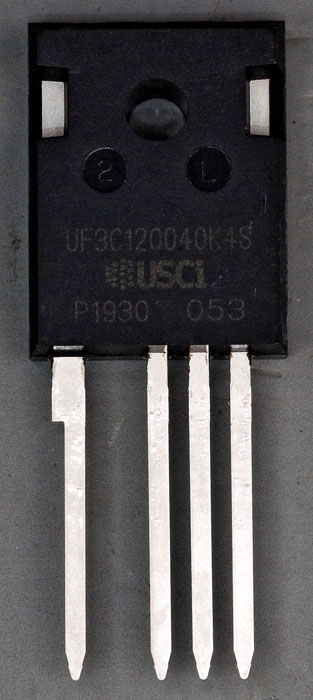
Recently I ordered a SiC-Cascode for burning it in my ofen...  >:D


A nice package for applications with higher voltages.
It also has a second source pin for more accurate gate control.
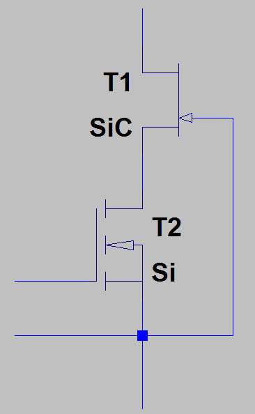


Manufacturing a SiC-J-FET is easier than a SiC-MOSFET. But for power electronics you usually want normaly off switches. Because of that UnitedSiC is building cascodes with a SiC-J-FET and a Si-MOSFET. With the Si-MOSFET we get the normal switching behaviour. Due to the SiC-J-FET the MOSFET has to carry the full current but only a small voltage.
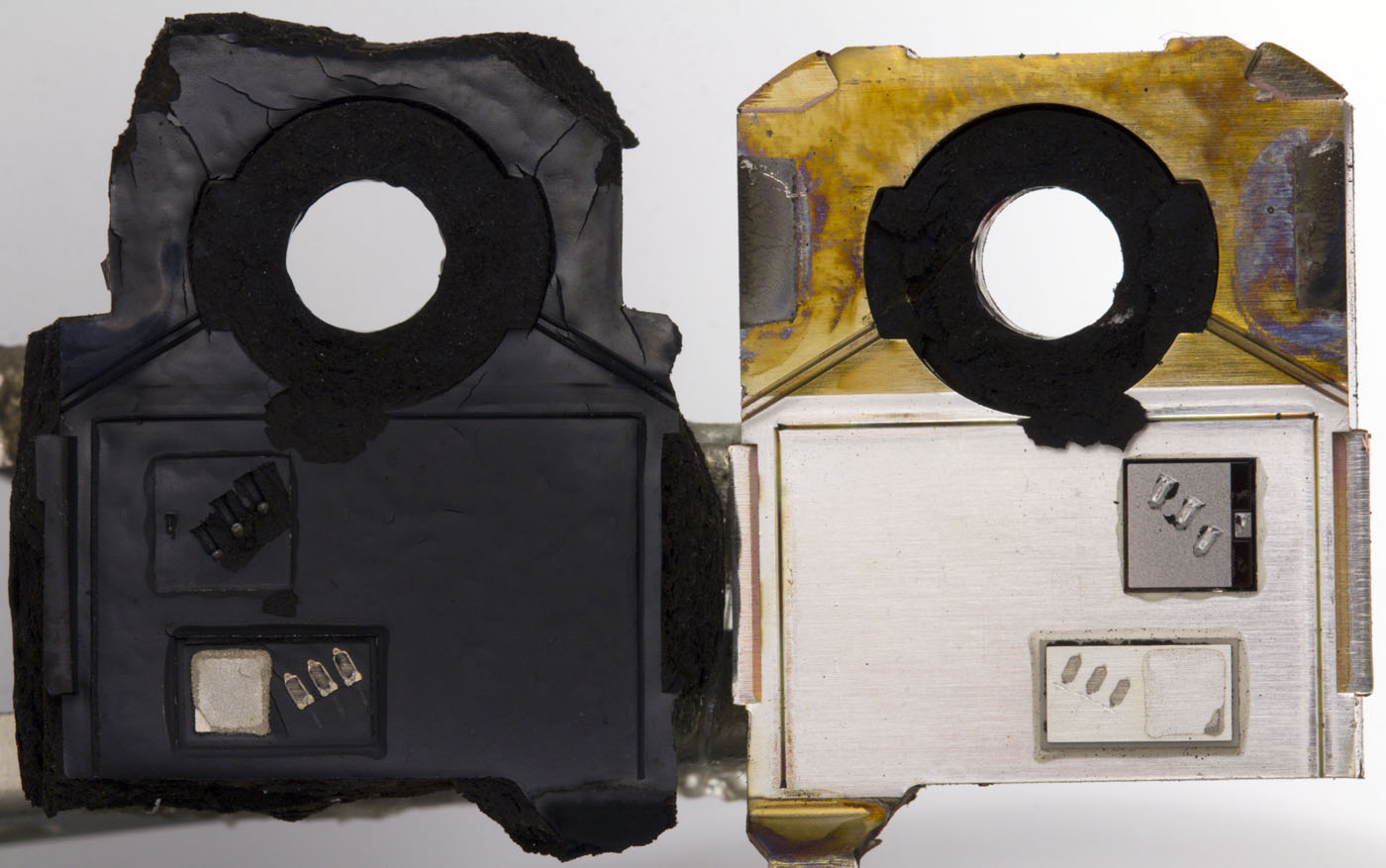


In the package we see the two dies. The lower MOSFET-die is still in the epoxy.
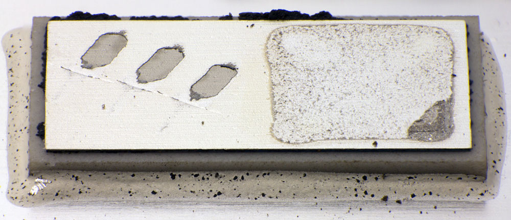


The MOSFET is placed on a ceramic insulator.
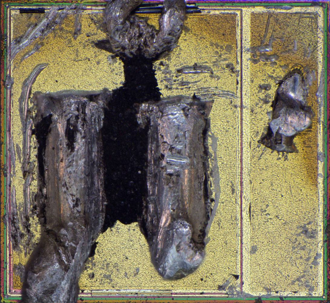


The MOSFET is quite small for this big bondwires!
It was not easy to clean the die and we can´t see very much of the mosfet. It´s clearly a low voltage mosfet because there is no bigger gap between the metal layer and the edge of the die.
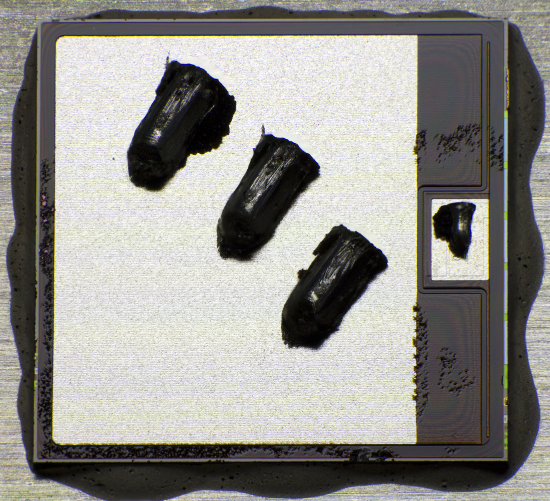
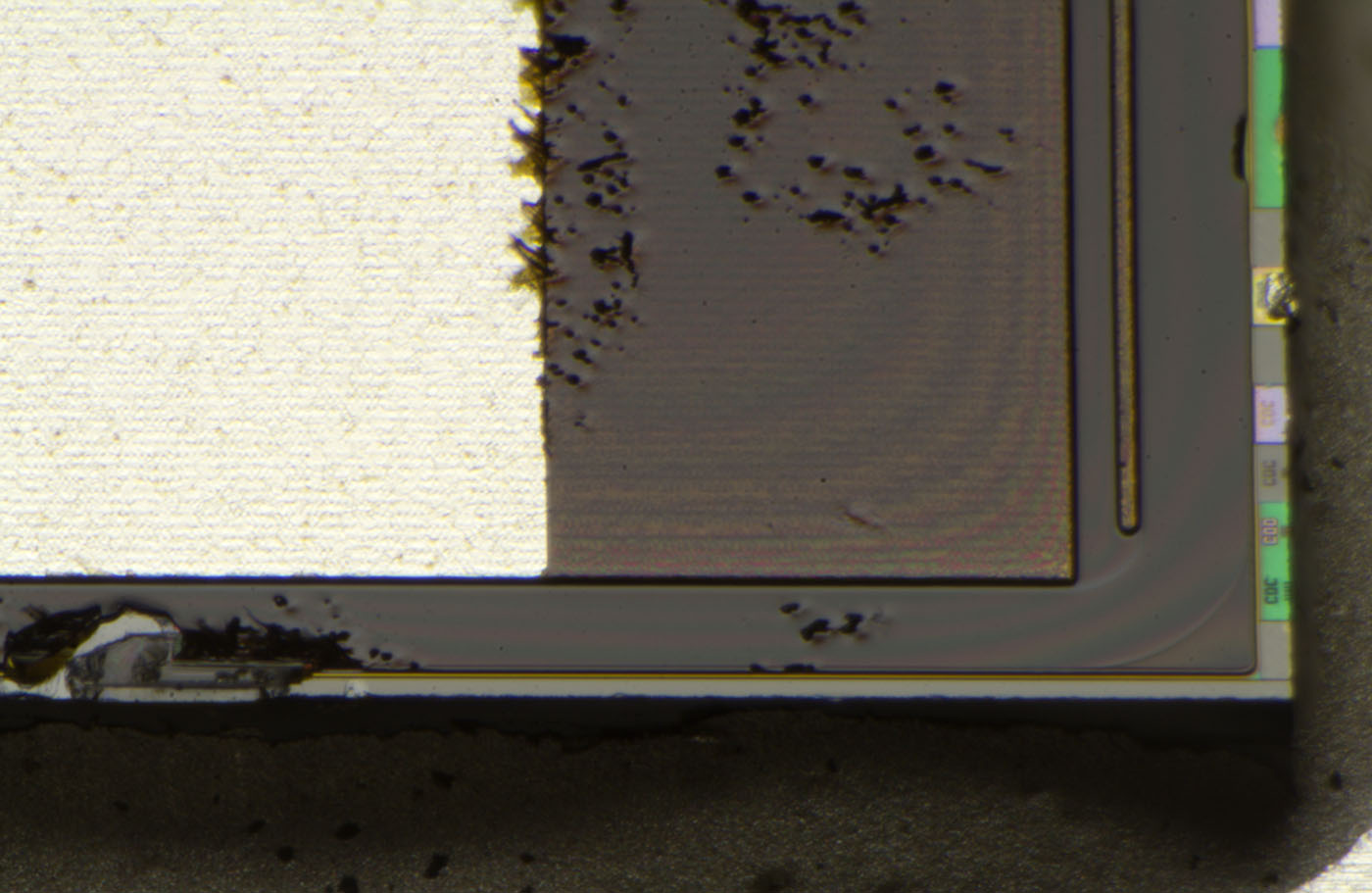


The SiC-FET-die is also not very spectacular, but...
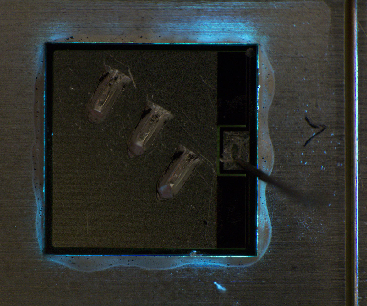


It glows blue when you put current over the gate-drain-junction!  8) 1A in this picture.
The forward voltage is 3,5V which is enough for blue light.


https://richis-lab.de/FET05.htm

 :popcorn:
 
The following users thanked this post: doktor pyta, Miyuki

Offline T3sl4co1l

  • Super Contributor
  • ***
  • Posts: 22436
  • Country: us
  • Expert, Analog Electronics, PCB Layout, EMC
    • Seven Transistor Labs
Re: Transistors - die pictures
« Reply #212 on: September 15, 2020, 08:27:02 pm »
Cool!  GaN FET next? :D

Tim
Seven Transistor Labs, LLC
Electronic design, from concept to prototype.
Bringing a project to life?  Send me a message!
 

Offline NoopyTopic starter

  • Super Contributor
  • ***
  • Posts: 1895
  • Country: de
    • Richis-Lab
Re: Transistors - die pictures
« Reply #213 on: September 15, 2020, 08:31:20 pm »
GaN is already sheduled!  :-+ ;D ...but it will take some time...
I also should take a closer look at a GaAs transistor...  :-/O

Offline exe

  • Supporter
  • ****
  • Posts: 2622
  • Country: nl
  • self-educated hobbyist
Re: Transistors - die pictures
« Reply #214 on: September 16, 2020, 09:31:10 am »
FERD diode please...
 

Offline NoopyTopic starter

  • Super Contributor
  • ***
  • Posts: 1895
  • Country: de
    • Richis-Lab
Re: Transistors - die pictures
« Reply #215 on: September 16, 2020, 10:16:54 am »
FERD diode please...

I can put it on my list.  :-+
(I still have some of your parts left...  ;))

Offline daqq

  • Super Contributor
  • ***
  • Posts: 2315
  • Country: sk
    • My site
Re: Transistors - die pictures
« Reply #216 on: September 16, 2020, 12:55:00 pm »
Awesome photos!

I'd love to see what's inside a Behlke module :)
Believe it or not, pointy haired people do exist!
+++Divide By Cucumber Error. Please Reinstall Universe And Reboot +++
 

Offline NoopyTopic starter

  • Super Contributor
  • ***
  • Posts: 1895
  • Country: de
    • Richis-Lab
Re: Transistors - die pictures
« Reply #217 on: September 16, 2020, 01:04:10 pm »
Thanks!  :-+ :)

The Behlke module seems a bit too big for my ofen...  ::)

Offline exe

  • Supporter
  • ****
  • Posts: 2622
  • Country: nl
  • self-educated hobbyist
Re: Transistors - die pictures
« Reply #218 on: September 16, 2020, 06:05:03 pm »
I can put it on my list.  :-+

Please do!
 

Offline NoopyTopic starter

  • Super Contributor
  • ***
  • Posts: 1895
  • Country: de
    • Richis-Lab
Re: Transistors - die pictures
« Reply #219 on: September 17, 2020, 08:55:45 pm »
I just did a small update of the ST Microelectronics TIP3055. I added a new (better) die picture:


https://www.richis-lab.de/Bipolar10.htm

Offline T3sl4co1l

  • Super Contributor
  • ***
  • Posts: 22436
  • Country: us
  • Expert, Analog Electronics, PCB Layout, EMC
    • Seven Transistor Labs
Re: Transistors - die pictures
« Reply #220 on: September 17, 2020, 10:17:50 pm »
That looks downright good, like, a... MJE15000-something? I already forget what else has the perf emitter... [well, the BUX22 most similarly, but other than that too]

Does that one measure well, particularly in terms of switching speed?  (Have you tried, or got more to test?)

Tim
Seven Transistor Labs, LLC
Electronic design, from concept to prototype.
Bringing a project to life?  Send me a message!
 

Offline NoopyTopic starter

  • Super Contributor
  • ***
  • Posts: 1895
  • Country: de
    • Richis-Lab
Re: Transistors - die pictures
« Reply #221 on: September 18, 2020, 03:16:40 am »
I have noted which transistor is using a perforated emitter in my overview:
https://www.richis-lab.de/Transistoren.htm
Sorry, german...  ;)

That is the:
2SC2922 (Sanken) https://www.richis-lab.de/2SC2922.htm
(The 2SC2922 is especially interesting because the perforation is different. Sanken is splitting the emitter in small areas.)
BD911 (ST) https://www.richis-lab.de/Bipolar12.htm
BUX22 new (ST) https://www.richis-lab.de/Bipolar08.htm
MJL21193 (ON) https://www.richis-lab.de/Bipolar15.htm
TIP2955 (ST) https://www.richis-lab.de/Bipolar11.htm
TIP3055 (ST) https://www.richis-lab.de/Bipolar10.htm

I didn´t test the switching speed but the TIP3055 is one of a batch that exe gave to me to take pictures. I think he did some measurements.
exe?

Offline exe

  • Supporter
  • ****
  • Posts: 2622
  • Country: nl
  • self-educated hobbyist
Re: Transistors - die pictures
« Reply #222 on: September 18, 2020, 09:26:59 am »
I didn´t test the switching speed but the TIP3055 is one of a batch that exe gave to me to take pictures. I think he did some measurements.
exe?

I did some measurements, not sure how accurate they are. I also cannot find measurements for tip2955, showing tip3055 here. I was choosing a bjt for a power supply. I wanted the fastest one, so I bought ten or twenty different bjts and measured them I simply hooked base to a siggen (ad2), and measured collector or emitter current with 1 Ohm shunt (I forgot which configuration I used for these plots). My figure of merit was frequency at which the phase shift reaches 45 degrees.

Conditions: collector current Ic=2A, Vce ~=1V (plus 2V drop on 1ohm resistor, that's why in filename it says "3V", that's total psu output).

As one may see, the 45 phase shift happens at following frequencies:
tip3055: 47 kHz
2ta1943: ~18kHz
2sd882: 450 kHz (this transistor is much less beefy than prev two, hence the difference)

NB: Increasing Vce often helps, but I wanted to see performance when Vce is 1V and less.
« Last Edit: September 18, 2020, 09:29:01 am by exe »
 

Offline T3sl4co1l

  • Super Contributor
  • ***
  • Posts: 22436
  • Country: us
  • Expert, Analog Electronics, PCB Layout, EMC
    • Seven Transistor Labs
Re: Transistors - die pictures
« Reply #223 on: September 18, 2020, 02:33:59 pm »
Hmm, do you know what h_fe was under that condition?

That should be the cutoff point, where it transitions from flat h_fe (from down to DC) to asymptotic (constant fT) behavior.  Which means fT = h_fe * Fc.

Tim
Seven Transistor Labs, LLC
Electronic design, from concept to prototype.
Bringing a project to life?  Send me a message!
 

Offline exe

  • Supporter
  • ****
  • Posts: 2622
  • Country: nl
  • self-educated hobbyist
Re: Transistors - die pictures
« Reply #224 on: September 18, 2020, 05:09:30 pm »
Hmm, do you know what h_fe was under that condition?

That should be the cutoff point, where it transitions from flat h_fe (from down to DC) to asymptotic (constant fT) behavior.  Which means fT = h_fe * Fc.

Tim

Looking at plots, I kind of see it. The top plot is gain in db, and one can see it 20db/decade (very roughly). That is, when frequency increases for 10x, the gain falls by factor of 10. I attach the picture where it's more obvious. For some reason there is raise in gain at the end of slope. May be there is some sort of cross-talk. I also notice that the yellow line (base current) goes down at high frequencies. I don't know if it's a measurement artefact, or it's Miller capacitance, or something, but for some transistors it is quite high. May be I'm overdriving avg on ad2 as it can only supply 10mA. I also use jumper wires, so I expect measurements above 1MHz are inaccurate.


I can repeat measurement in a more controlled environment if one wants. I also ordered a few more transistors to see how they perform: D44H8, D45VH10G, D45H8G, D45H11G,  MJF45H11G, 2SD1060S-1E, KSE44H11, BD911, BD912,  D45H11FP and KSB772YS .


Share me

Digg  Facebook  SlashDot  Delicious  Technorati  Twitter  Google  Yahoo
Smf