Author Topic: Transistors - die pictures  (Read 247612 times)

0 Members and 2 Guests are viewing this topic.

Offline NoopyTopic starter

  • Super Contributor
  • ***
  • Posts: 1883
  • Country: de
    • Richis-Lab
Re: Transistors - die pictures
« Reply #725 on: June 17, 2023, 06:05:45 am »
How is the SCT2450KE bonded to its package? I didn't see a leadframe.

There was a normal leadframe, nothing special. The die just didn't remain on the leadframe.
« Last Edit: June 17, 2023, 06:14:16 am by Noopy »
 

Offline NoopyTopic starter

  • Super Contributor
  • ***
  • Posts: 1883
  • Country: de
    • Richis-Lab
Re: Transistors - die pictures
« Reply #726 on: June 17, 2023, 06:22:25 am »
Very cool!  AFAIK, SiC are currently not Superjunction, just traditional planar stripe VDMOS or whatever.  The top grid pattern presumably is source connections (vias) dipping down to the die surface, through a grid (square mesh?) of gate connections.  Analogous to ye olde HEXFETs, as far as the top interconnect goes.  But with a square grid, and I assume a vertical trench structure below.  It's not clear if the FET cells would also be on a square grid, or are just stripes the whole width.

I agree with your interpretation.  :-+
But I don´t know if they even use trenches in SiC. Would be nice to have but I don´t know if that is already possible with SiC technology.


The size comparison is particularly apt, as the Si chips are also traditional planar technology -- which puts them at particular disadvantage at the higher voltage ratings.  For that technology, specific Rds(on) scaled something like Vds^2.2.

Thanks to the high breakdown field strength, comparable geometry (e.g. junction depletion widths) would give more like a 100V rating in Si, but more like 1000V in SiC.  That's basically a IRF520!

 :-+


Oh! I don't suppose that's still working to some extent?  Maybe not after the acid dip, but, I wonder if the body diode glows in forward bias? >:D

Well after furnace decapping lighting a junction should still be possible (like here: https://www.richis-lab.de/FET05.htm).
And of course I tried that with the SCT2450KE too. Unfortunately nothing happened. Perhaps I didn´t get good contact. Perhaps there was some major damage. I don´t know. I was very sad...  :'( ;D

Offline NoopyTopic starter

  • Super Contributor
  • ***
  • Posts: 1883
  • Country: de
    • Richis-Lab
Re: Transistors - die pictures
« Reply #727 on: July 04, 2023, 08:35:55 pm »


A new 2N3055! This one is built by Sescosem.
Since I didn´t find a datasheet I don´t know what TVCD means.  :-//


There is a heatspreader in the package that takes up almost the entire area. A relatively large amount of solder was used to attach the die to the heatspreader.


The transistor has a MESA structure and is covered with a transparent protective coating. At the lower edge you can see that it wasn´t cut out of the wafer a clean as they do it today.


The MESA structure is clearly visible.


There are some relatively deep holes on the MESA edge. The etching process of the MESA structure does not seem to have been very accurate.


In the upper left corner you can see an impressive manufacturing defect. A large trench has formed parallel to the MESA structure. The trench is so close to the active area that the metal layer in this corner became very narrow.


The surface of the transistor has no unusual structures. Under the outer metal surface, the contact area to the silicon seems to be somewhat larger than necessary. Towards the base-emitter interface, its edge can be seen a little.


For an epitaxial transistor, the breakdown of the base-emitter path occurs relatively late at -15V. This can probably be explained by the fact that this is an early model of an epitaxial transistor. Compared to modern transistors with their much more clean processes, the concentration of dopants had to be chosen lower in the past.

In the picture above, the current increases as follows: 5mA, 10mA, 20mA, 30mA, 40mA, 50mA, 100mA, 200mA, 300mA. The luminous effect is distributed fairly evenly across the junction.


Operation in the breakdown shows a strikingly large disturbance in the junction. The current flow you can see here is 100mA, 200mA, 300mA, 400mA, 500mA.


The semi-circular glow forms around a round disturbance near the junction. Many optical artefacts are merely impurities on the surface of the transistor or the protective coating. Here, however, there is actually a disturbance in the active area. It is impossible to be sure what is happening in this area. In any case, the junction has expanded to the right. It could be that the circle contains the emitter doping that has entered the base area due to a weakness in the manufacturing process.

In the lower area on the left side there is another disturbance, which is only noticeable by a relatively bright dot. This is probably a minor irregularity as seen in the BUX22 built by ST Microelectronics (https://www.richis-lab.de/Bipolar07.htm#defect).


The prolonged operation in the base emitter breakdown ultimately destroyed the junction in the lower left corner.

In detail, you can see that the surface on the edge of the outer metallisation has also been etched in the form of the MESA structure.


The path along which the current has concentrated after the junction has collapsed is clearly visible. Both on the side of the base and on the side of the emitter, a path can be seen that leads to the junction. The metal layer has melted on both sides and cracks can be seen in the surface between them.

Due to the damage, the contact area in the passivation layer is now also more clearly visible. Inside the recess, the silicon has melted a little. Presumably it has entered into an alloy with the metal layer. Where the passivation layer begins, the current path appears greenish. Following this, the current path narrows and the current density increases. According to the optical appearance, the material is more damaged in this area. The emitter area seems to be less damaged, perhaps because of the higher doping.


https://www.richis-lab.de/2N3055_17.htm

 :-/O
 
The following users thanked this post: SeanB, exe, RoGeorge, karpouzi9

Offline T3sl4co1l

  • Super Contributor
  • ***
  • Posts: 22368
  • Country: us
  • Expert, Analog Electronics, PCB Layout, EMC
    • Seven Transistor Labs
Re: Transistors - die pictures
« Reply #728 on: July 04, 2023, 08:46:49 pm »
I hope you weren't using a bench supply (CC/CV with big capacitor on the output) for that test...were you?  :horse:

Tim
Seven Transistor Labs, LLC
Electronic design, from concept to prototype.
Bringing a project to life?  Send me a message!
 

Offline NoopyTopic starter

  • Super Contributor
  • ***
  • Posts: 1883
  • Country: de
    • Richis-Lab
Re: Transistors - die pictures
« Reply #729 on: July 04, 2023, 08:55:12 pm »
I hope you weren't using a bench supply (CC/CV with big capacitor on the output) for that test...were you?  :horse:

Tim

 ;D
That wasn´t the problem. The problem was to much heat. I try to take the pictures without a bulky heatsink. Most of the time that works quite well but sometimes I´m too impatient and even a few watt generate a lot of heat...  >:D

Offline T3sl4co1l

  • Super Contributor
  • ***
  • Posts: 22368
  • Country: us
  • Expert, Analog Electronics, PCB Layout, EMC
    • Seven Transistor Labs
Re: Transistors - die pictures
« Reply #730 on: July 04, 2023, 10:10:05 pm »
I know, for the initial failure it's just straight up heat; I mean the subsequent melting. >:D

Tim
Seven Transistor Labs, LLC
Electronic design, from concept to prototype.
Bringing a project to life?  Send me a message!
 

Offline NoopyTopic starter

  • Super Contributor
  • ***
  • Posts: 1883
  • Country: de
    • Richis-Lab
Re: Transistors - die pictures
« Reply #731 on: July 05, 2023, 03:30:00 am »
I assume concentrating the power at such a small area would melt the structures independent of the bench supply.
...but yes, it was the cheap one...  ;D

Offline NoopyTopic starter

  • Super Contributor
  • ***
  • Posts: 1883
  • Country: de
    • Richis-Lab
Re: Transistors - die pictures
« Reply #732 on: July 13, 2023, 12:54:25 pm »


The BUX37 is a Darlington transistor with an integrated free-wheeling diode. The present model was produced by Thomson Semiconducteurs in 1980. The transistor blocks up to 400V and conducts up to 15A. If the case temperature remains below 100°C, up to 35W can be dissipated. The current gain is at least 20.


In the package there is a large heatspreader. Channels in the heatspreader allow excess solder to flow off.


The dimensions of the die are 6,0mm x 5,5mm. A transparent varnish protects the transistor against environmental influences. The particles on the protective varnish were created while opening the case.


It is obviously a MESA transistor. From the outside to the inside, parts of the surface have turned brown.


The protective coating can be removed relatively easily, allowing an unobstructed view of the structures.


The driver transistor is located in the right area (yellow), the transistor of the power path is integrated in the left area (red). The free-wheeling diode and the resistors are not visible here. A more detailed description of the structure and operation of such a Darlington transistor can be found within the documentation of the SU111 (https://www.richis-lab.de/Bipolar59.htm).


Under the thick protective coating, there is obviously an additional thin passivation layer on the transistor. Either the coating itself has turned brown or there is contamination underneath. Brown degradation of the silicon seems rather unlikely.

The outer edges of the transistor are very rough. It could be that the surface has been scored for singulation. In the valley of the MESA structure an additional step can be seen.


Some spots give the impression that the degradation has penetrated into the area of the semiconductor and not only has changed the protective layer. However, it could be that the passivation has changed especially at edges and that is why it looks like this.


https://www.richis-lab.de/BipolarA34.htm

 :-/O
 
The following users thanked this post: SeanB, RoGeorge, ch_scr

Offline T3sl4co1l

  • Super Contributor
  • ***
  • Posts: 22368
  • Country: us
  • Expert, Analog Electronics, PCB Layout, EMC
    • Seven Transistor Labs
Re: Transistors - die pictures
« Reply #733 on: July 13, 2023, 03:01:50 pm »
I wonder how they implemented the diode. P-region buried under the emitter contact, perhaps?  There's a faint outline under the emitter metal, but that could just be connections.

I wonder if a parasitic SCR (PNPN) breakdown mode could be activated, say with large dV/dt, or forward or reverse avalanche...

Tim
Seven Transistor Labs, LLC
Electronic design, from concept to prototype.
Bringing a project to life?  Send me a message!
 

Offline NoopyTopic starter

  • Super Contributor
  • ***
  • Posts: 1883
  • Country: de
    • Richis-Lab
Re: Transistors - die pictures
« Reply #734 on: July 13, 2023, 03:19:09 pm »
I wonder how they implemented the diode. P-region buried under the emitter contact, perhaps?  There's a faint outline under the emitter metal, but that could just be connections.

I assume that's the same as with the SU111:
https://www.eevblog.com/forum/projects/transistors-die-pictures/msg3585647/#msg3585647


I wonder if a parasitic SCR (PNPN) breakdown mode could be activated, say with large dV/dt, or forward or reverse avalanche...

I don't see an SCR but with that much p and n you can never be sure.

Offline T3sl4co1l

  • Super Contributor
  • ***
  • Posts: 22368
  • Country: us
  • Expert, Analog Electronics, PCB Layout, EMC
    • Seven Transistor Labs
Re: Transistors - die pictures
« Reply #735 on: July 13, 2023, 03:24:36 pm »
Ah, right, they could use the base layer; which also implements the B-E resistor, assuming the resistivity and geometry of the layer works out (which seems to be the case). Nice. :)

Any PNPN behavior would be driven by lateral motion, which is probably a very long shot over the width of this die, yeah.

Tim
Seven Transistor Labs, LLC
Electronic design, from concept to prototype.
Bringing a project to life?  Send me a message!
 

Offline NoopyTopic starter

  • Super Contributor
  • ***
  • Posts: 1883
  • Country: de
    • Richis-Lab
Re: Transistors - die pictures
« Reply #736 on: July 13, 2023, 03:35:32 pm »
These integrated Darlingtons are really a piece of art. A simpel looking piece of art but nevertheless a piece of art.  8)
 
The following users thanked this post: SeanB, T3sl4co1l, karpouzi9

Offline NoopyTopic starter

  • Super Contributor
  • ***
  • Posts: 1883
  • Country: de
    • Richis-Lab
Re: Transistors - die pictures
« Reply #737 on: August 04, 2023, 03:56:51 am »


The Intersil CA3096 is a transistor array with three NPN and two PNP transistors. The maximum collector-emitter voltage is at least 45/40V (NPN/PNP). Collector currents up to 50/10mA are specified. The current gain at a collector current of 1mA is in the range of 150-500 / 20-200.

The variant with the index A is an assortment with more closely specified characteristics. Less precisely specified variants carry the index C. The present component, without an index at this point, represents the basic variant. The second letter, here an E, stands for the housing variant.


The marking makes a somewhat unclean impression. However, as we will soon see, it is in fact a CA3096.


The datasheet contains a picture of the metal layer showing the arrangement of the transistors and the dimensions.


The edge length of the die is 0,99mm. 6270 is most likely the internal project designation. In the lower right area there is a structure with a cross that makes it possible to check the alignment of the masks against each other.

The NPN and PNP transistors show the familiar structure. Since PNP transistors in an NPN process are less efficient, they had to be made much larger. Each PNP transistor consists of seven individual elements. This is the only way to achieve reasonably similar specifications.

The datasheet contains typical offset values for the case that one sets up a differential amplifier with the Q1/Q2 or Q4/Q5 transistors. The offset voltage of the PNP version is somewhat lower than that of the NPN version. The significantly larger areas of the PNP transistors ensure that the real base-emitter voltages that occur are closer to the typical value. With the smaller NPN transistors, the scattering of the doping has a greater effect.


https://www.richis-lab.de/BipolarA35.htm

 :-/O
 
The following users thanked this post: SeanB, doktor pyta, TurboTom, exe, Wolfgang, RoGeorge, ch_scr, slavoy

Offline NoopyTopic starter

  • Super Contributor
  • ***
  • Posts: 1883
  • Country: de
    • Richis-Lab
Re: Transistors - die pictures
« Reply #738 on: August 07, 2023, 04:24:23 am »


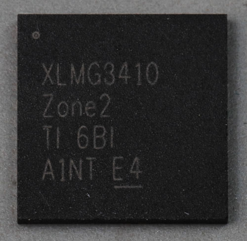
The LMG3410 from Texas Instruments is a transistor based on gallium nitride (GaN). Like silicon carbide, the semiconductor material gallium nitride has a large bandgap and is therefore very well suited to switching high voltages and high currents quickly and with low losses. Compared to SiC, the maximum permissible reverse voltage of GaN transistors is usually somewhat lower, but GaN transistors can be switched faster. In addition to a GaN power transistor, the LM3410 contains a driver and a silicon MOSFET, so that control is relatively straightforward.

Up to 480V can be applied to the LMG3410 continuously. The absolute maximum ratings specify 600V and even 800V transiently. The 800V pulses may only occur one million times. Edge steepnesses of up to 150V/ns are permissible. At a junction temperature of 125°C, 12A is specified as the maximum current flow. At 25°C, the Absolute Maximum Ratings specify up to 40A. Pulses applied for less than 100ns may rise to 100A. The resistance in the active state is given as 70mΩ/110mΩ (25°C/125°C).

The output capacitance of the GaN transistor is 71pF. However, the absence of a body diode is particularly interesting, which is why the reverse recovery charge can be specified as 0nC. This means that in the application in a half- or H-bridge, the reverse charge is much less critical. Although a GaN FET does not have an intrinsic diode like a silicon MOSFET, operation in the third quadrant, i.e. current flow from source to drain, is still possible.


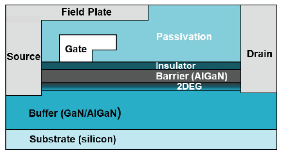
The above image is from an application report by Texas Instruments ("Does GaN Have a Body Diode? - Understanding the Third Quadrant Operation of GaN"). It shows how a GaN transistor can be constructed. A GaN transistor is a so-called HEMT, a High Electron Mobility Transistor. In it, one area contains a so-called two-dimensional electron gas ("2DEG"), in which electrons can flow with very little resistance.

On Wikipedia you can read that it is a special form of the MESFET, i.e. a J-FET in which the channel is not constricted by an inverse doping but by a metal contact. In the meantime, however, there are also variants with an insulated gate electrode. The sectional view shown here appears to contain such an insulating layer. The extension of the source and gate lead controls the electric field in the active area, resulting in a higher dielectric strength.


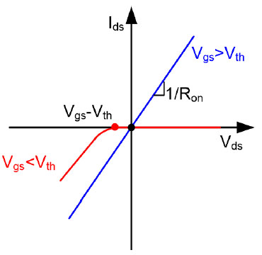
Texas Instruments also explains in the above document why GaN transistors behave as if they contain a body diode. If Vgs is above Vth, current can flow through the device in both directions (blue). If Vgs is below Vth (red), the transistor blocks positive Drain-Source voltages. If Vds is negative, however, the transistor becomes conductive again. The negative drain potential leads to a positive Gate-Drain voltage, which has the same effect in the third quadrant as a positive Vgs in the first quadrant. However, the characteristic curve is shifted by Vgs-Vth and the channel resistance is slightly higher.

Compared to a MOSFET with a body diode, the voltage drop across a GaN transistor in the third quadrant is relatively high. The LMG3410 datasheet specifies 7,8V at a current flow of 10A. This results in correspondingly high losses. Either the current-time area should be kept small in this quadrant or the transistor should be switched on.


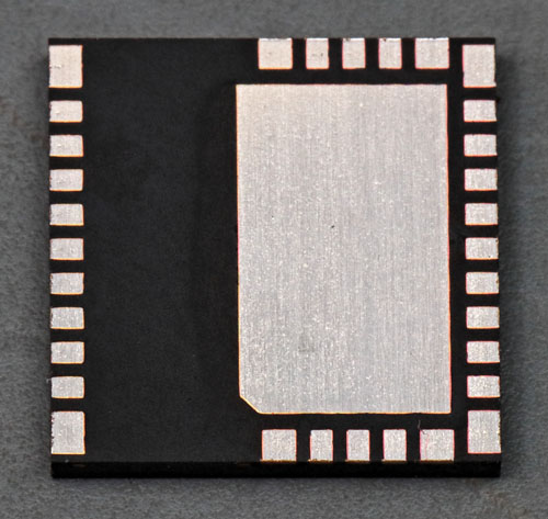
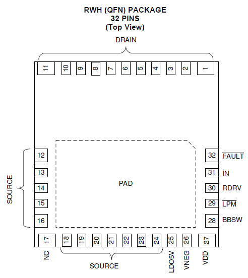
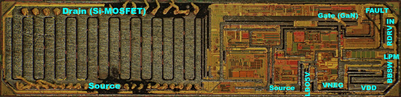
The transistor is in a VQFN package with an exposed pad. The datasheet shows the pinning of the LMG3410. The upper contacts all carry the drain potential. The lower area has a similar number of contacts for the source potential. In addition, there are pins for the supply and the control of the transistor.


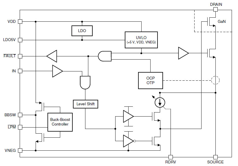
The datasheet contains a block diagram showing how the LMG3410 works. As with SiC transistors, the first GaN FETs were exclusively normally on. Here, such a normally on GaN FET is used. If you still want intrinsically safe behaviour, you can build a cascode, as in the case of the UnitedSiC UF3C120040K4S (https://www.richis-lab.de/FET05.htm). In the case of the LMG3410, a more complex approach has been taken. There is a normal Si MOSFET in series with the GaN transistor. Here, however, the two transistors do not form a cascode circuit, but are controlled independently of each other.

The LMG3410 requires a supply voltage between 9,5V and 18V. From this, a linear regulator generates a 5V supply for the controller. A switching regulator also generates a negative supply of -13,9V to safely switch off the GaN transistor. The current consumption is typically 43mA.

A push-pull stage either connects the gate of the GaN transistor to the source potential, thus making it conductive, or it connects the gate to the negative supply, thus switching it off. A resistor on pin RDRV allows the switching speed to be varied between 30V/ns and 100V/ns. The LMG3410 contains both an overcurrent and an overtemperature monitor that protects the device against overload.

If the LMG3410 is in the idle state (current consumption 80µA) or is not supplied, the Si MOSFET is switched off and the gate of the GaN transistor is connected to the source terminal of the device. In this state, the voltage across the Si MOSFET rises until the gate of the GaN transistor becomes so negative that it also blocks and thus carries most of the blocking voltage. In the meantime, it is possible to produce normally off GaN FETs too, which simplifies safe application.


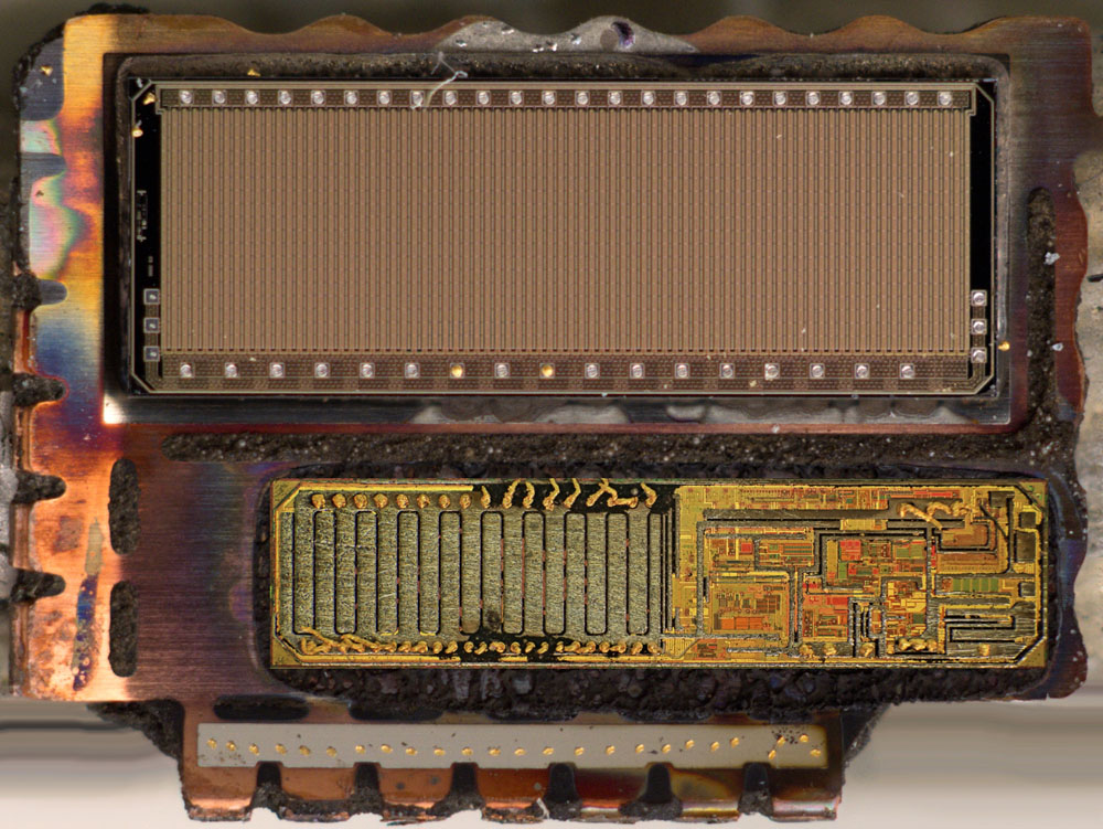
There are two dies in the package. The upper die is the GaN transistor (5,8mm x 2,1mm). The lower die is the control circuit, which also contains the Si MOSFET (5,2mm x 1,3mm). The control circuit detached from the carrier when the package was opened. It was later reinserted into the picture.


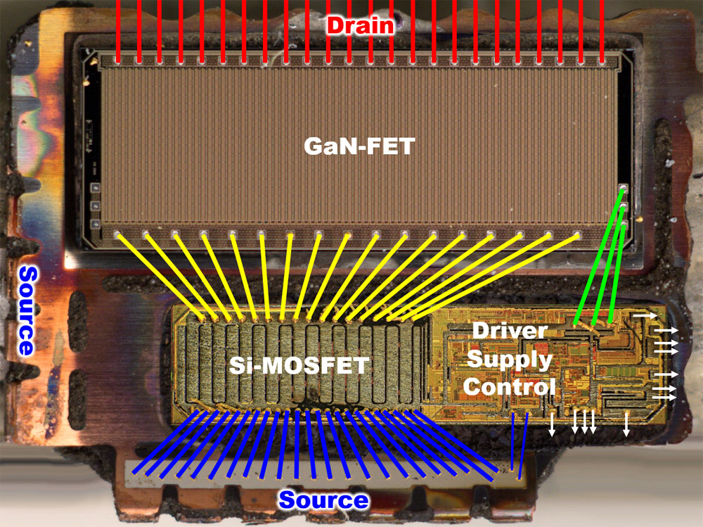
The bondwires can be reconstructed quite easily. GaN transistors usually conduct the current laterally. Here, the Si MOSFET is also constructed laterally. This is possible quite efficiently because the Si MOSFET must be able to carry the full current of the LMG3410 (40A), but no high blocking voltage rating is necessary. Probably a little more than 20V should be sufficient.


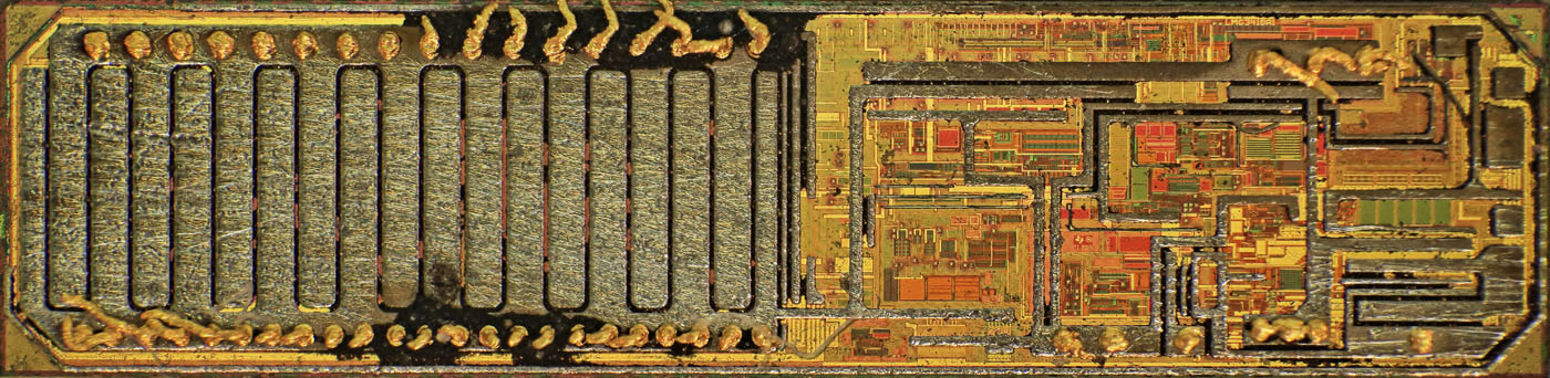
Half of the area of the control circuit is taken up by the Si MOSFET. The other half contains the supply circuits, the control and the drivers.


The die is 0,25mm thick and carries a very solid metal layer with a height of about 11µm.


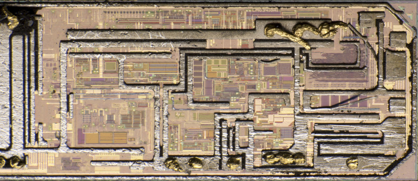
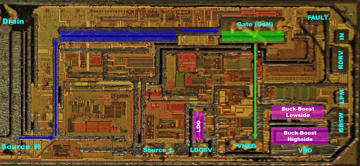
The structures of the control system are too small and too complex to be analysed in detail. However, some function blocks can be identified on the basis of the massive lines. The linear regulator of the 5V voltage regulator can be recognised by its contacting, as can the highside and the lowside transistor of the buck-boost converter (pink).

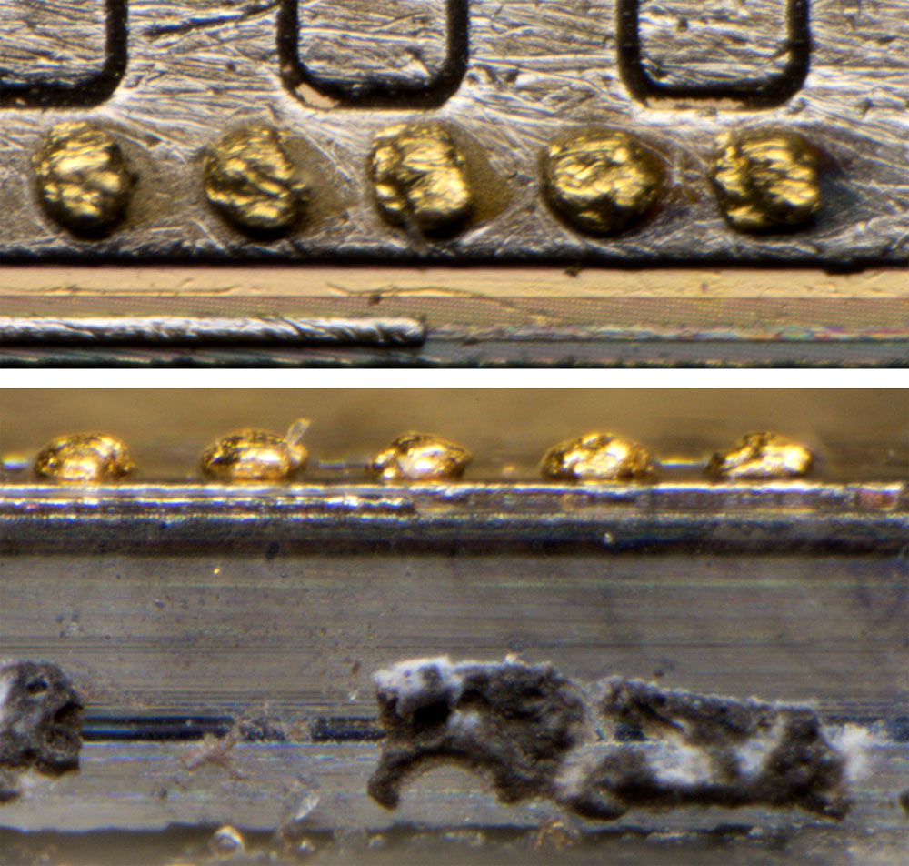
The gate contact of the GaN FET is connected to the source potential of the component via a very large transistor (blue). Another, not quite as large transistor connects the gate to the negative supply potential (green). The source potential is connected to the die via two paths. A whole row of bondwires leads to the Si MOSFET. Three more bondwires connect the control circuit to the source potential of the device. This keeps interference from the power path away from the control circuit.


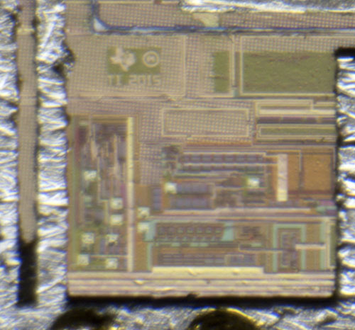
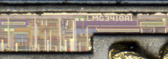
The design obviously dates from 2015 and the designation LMG3410A1 can be found on the die. A1 could stand for a first revision.

The LMG3410 switches off in case of an overcurrent event and remains switched off. The LMG3411 is listed in the same datasheet. However, in the event of an overcurrent this device switches off just for the current cycle. Most likely, the LMG3411 uses the same controller, which is simply configured differently in production.


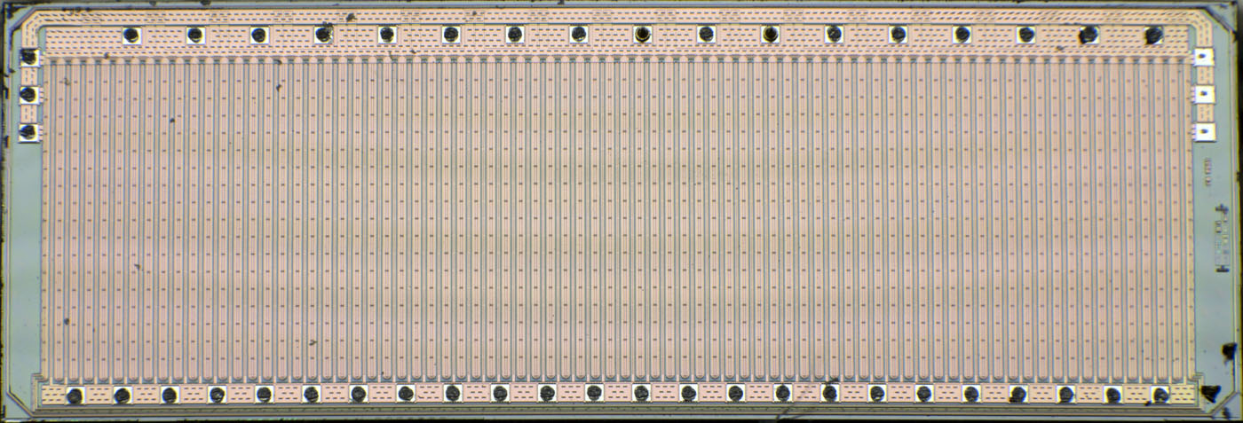
In this picture the GaN transistor is rotated 180° compared to the pictures above. It has a whole row of drain and source bondpads. On the left and right, you can contact the gate potential via three bondpads each, whereby only the left contacts are used in the LMG3410.


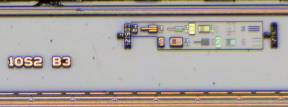
On the right edge, in addition to some designations, the masks are shown too.


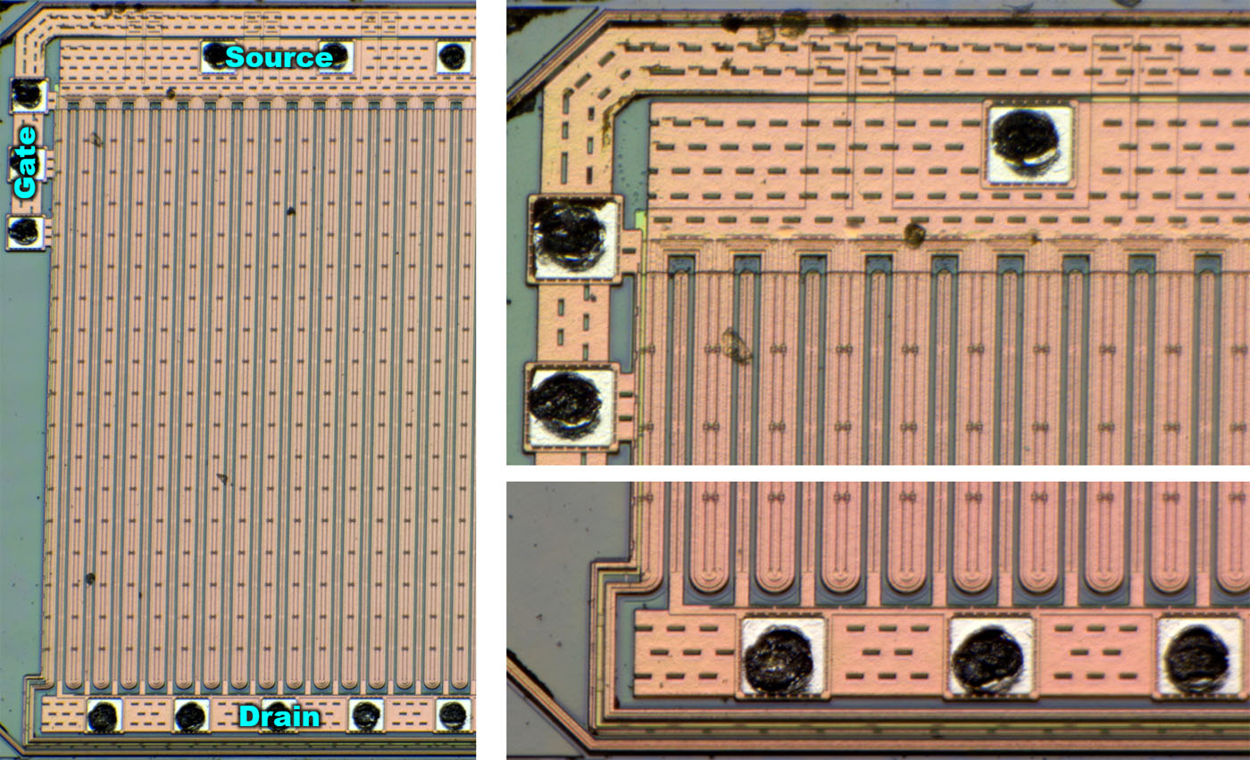
The drain potential is flanked by the source potential over the entire circumference. Regular undercrossings of the wide source lines lead the gate potential into the active area.


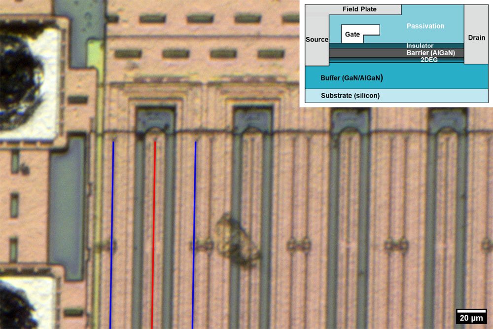
The structures can be easily identified by looking at the structure published by Texas Instruments. Thin vertical lines form the contacts of the source (blue) and drain (red) to the active area. The source metal line is wider. Underneath is the gate electrode.


https://www.richis-lab.de/FET33.htm

 :-/O
 
The following users thanked this post: SeanB, Vgkid, T3sl4co1l, TurboTom, RoGeorge, Miyuki, ch_scr, MegaVolt

Online RoGeorge

  • Super Contributor
  • ***
  • Posts: 6701
  • Country: ro
Re: Transistors - die pictures
« Reply #739 on: August 07, 2023, 05:30:23 am »
Thanks for the pics.  :-+
As TI wrote on it, it is now clear this AINT E4;D

Offline NoopyTopic starter

  • Super Contributor
  • ***
  • Posts: 1883
  • Country: de
    • Richis-Lab
Re: Transistors - die pictures
« Reply #740 on: August 16, 2023, 08:03:17 pm »


The RCA 2N3670 is a thyristor designed for use in 240V power supplies. A peak voltage of 400V is permissible on a permanent basis. For short periods, the reverse voltage may rise to 660V. An effective value of 12,5A and a peak value of 200A are specified for the current flow.

In addition to the 2N3670, the data sheet lists the three similar variants 2N3668, 2N3669 and 2N4103 with different blocking voltages (100V, 200V, 600V).


The electrical contacting is similar to that of germanium power transistors. The cathode potential is supplied from the left. The gate potential is transferred by a metal strip from the right to the centre of the assembly. Here, however, the semiconductor rests almost directly on the bottom of the housing and there is a metal ring above it. It could be that the ring not only bridges the distance between the semiconductor and the contact plate, but is also necessary to distribute the current evenly over the semiconductor.


Inside the metal ring, you can see the semiconductor itself between the gate contact in the middle and the outer cathode contact.


The protective lacquer obscures the view of the active area. You still can see the approximately 0,15mm thick semiconductor disc. There is a layer of solder above and below it. In the bottom of the base plate there is a flat socket.


https://www.richis-lab.de/BipolarA36.htm

 :-/O
 
The following users thanked this post: SeanB, TurboTom, RoGeorge, Miyuki, ch_scr

Offline NoopyTopic starter

  • Super Contributor
  • ***
  • Posts: 1883
  • Country: de
    • Richis-Lab
Re: Transistors - die pictures
« Reply #741 on: August 18, 2023, 04:02:22 am »


The KF517 is a PNP small signal transistor built by Tesla. Vceo is 30V. The collector current may be up to 500mA. The datasheet specifies a cut-off frequency of at least 50MHz. Without additional cooling, a power dissipation of 0,8W can be dissipated, with ideal cooling, 2,6W is possible. FX stands for production in May 1974. Although there is no index here, the KF517 have been sorted by their amplification factor: A offers a gain factor between 35 and 120, B guarantees 90 - 300 and C is specified with 60 - 160.


The edge length of the die is 1,0mm. The bondwires are welded to the metal layer in two places. The structures do not show any special features. The emitter surface appears brown. Around the emitter, the dark green base area can be seen, which is also located below the emitter. Below this, in turn, extends the collector area, which is recognisable around the base area in a somewhat lighter green. In the outer area are the usual simple auxiliary structures.


The base-emitter junction breaks down at 15V. If the transistor is operated with limited current in this area, the familiar glowing appears. At 10mA, the glow is still sporadic but already very uniform. From 20mA over 50mA, the glow spreads until at 100mA the junction on the surface lights up completely.  8)


https://www.richis-lab.de/BipolarA37.htm

 :-/O
 
The following users thanked this post: SeanB, TurboTom, RoGeorge, ch_scr

Offline konohimawm

  • Newbie
  • Posts: 5
  • Country: tr
    • Signal Elektronik
Re: Transistors - die pictures
« Reply #742 on: August 18, 2023, 11:02:32 am »
I like Tesla KF517 so clean    :-+
 

Online TurboTom

  • Super Contributor
  • ***
  • Posts: 1428
  • Country: de
Re: Transistors - die pictures
« Reply #743 on: August 19, 2023, 12:27:34 am »
The wrinkled bond wires made me laugh... But I guess that's just a collateral of cutting the case open. Very well done, Noopy, I really enjoy your contributions! Thanks so much for this  :-+
 

Offline NoopyTopic starter

  • Super Contributor
  • ***
  • Posts: 1883
  • Country: de
    • Richis-Lab
Re: Transistors - die pictures
« Reply #744 on: August 19, 2023, 03:08:19 am »
It is a pleasure!  8)  I still have pretty much to do.  :-/O

Actually i didn´t touch the bondwires. They are like they were before.  ;D
 
The following users thanked this post: TurboTom

Offline NoopyTopic starter

  • Super Contributor
  • ***
  • Posts: 1883
  • Country: de
    • Richis-Lab
Re: Transistors - die pictures
« Reply #745 on: August 24, 2023, 07:26:47 pm »


Here we have another BUX22. This BUX22 from ST Microelectronics seems to be newer than the refurbished BUX22 from 1988, whose initial marking still has an old format (https://www.richis-lab.de/Bipolar07.htm). At the same time, it is older than the BUX22 with the perforated emitter (https://www.richis-lab.de/Bipolar08.htm), since it still has the relatively thick, structured base plate.


As with the other BUX22, two dies were used here. The bondwires are not as unusually thick as in the refurbished BUX22 from 1988, but the emitters were contacted with two bondwires each.


It is a challenge to route the four emitter bondwires without collision in the limited volume and to connect them to the corresponding pin. In order to be able to weld all the wires at all, they have been lined up at the side of the connection pin.


In contrast to the newer BUX22 with the perforated emitter, classic transistor structures were used in this BUX22.


The BUX22 seen here does not contain an additional heatspreader due to the massive baseplate of the package. As with the refurbished BUX22 from 1988, however, there are metal plates under the dies. The different thermal expansion coefficients of the silicon and the base plate create mechanical stresses. The metal plates can absorb these tensions or equalize the different thermal expansion coefficients.


The transistors do not show any unusual structures, even in detail.


As with the other BUX22, the base-emitter junction breaks down relatively late. Here the breakdown voltage is -15V. The current rises from 10mA to 100mA to 500mA to 1A.

The glow speaks for a relativ even current distribution between the two transistors. On the die, the glow occurs first and intensified to the left of the emitter contact area.


https://www.richis-lab.de/BipolarA38.htm

 :-/O
 
The following users thanked this post: SeanB, doktor pyta, TurboTom, RoGeorge, floobydust, Miyuki, ch_scr, iMo

Offline floobydust

  • Super Contributor
  • ***
  • Posts: 7426
  • Country: ca
Re: Transistors - die pictures
« Reply #746 on: August 24, 2023, 07:58:53 pm »
BUX22 rated 250V 40A 350W hFE 20-60, fT 10MHz "silicon multiepitaxial planar NPN".
 

Offline NoopyTopic starter

  • Super Contributor
  • ***
  • Posts: 1883
  • Country: de
    • Richis-Lab
Re: Transistors - die pictures
« Reply #747 on: August 24, 2023, 08:05:00 pm »
BUX22 rated 250V 40A 350W hFE 20-60, fT 10MHz "silicon multiepitaxial planar NPN".

Peak current 50A (10ms).
 
The following users thanked this post: SeanB, TurboTom

Offline NoopyTopic starter

  • Super Contributor
  • ***
  • Posts: 1883
  • Country: de
    • Richis-Lab
Re: Transistors - die pictures
« Reply #748 on: August 30, 2023, 04:06:24 am »


The BD115 is an early silicon transistor that can block up to 180V. The development goes back to Valvo. Today, there are also models from younger manufacturers such as CDIL. This transistor has no logo and no manufacturer's name, but it seems to be very old, which indicates that it was made by Valvo.

The specified reverse voltage shows that it is still an early process. While the collector-base breakdown voltage is 245V, the collector-emitter breakdown voltage is specified with just 180V. At this voltage, the collector-base leakage current already increases so much that the transistor is overloaded. The datasheet gives a value of 0,55mA for a reverse voltage of 200V and a junction temperature of 200°C. At this operating point, 110mW are generated in the transistor.

The collector current may be up to 150mA. At a case temperature of 100°C, the TO-39 case can dissipate up to 6W. The DC gain is specified as 60 (100V/50mA). The cut-off frequency is 145MHz.


The actual transistor is located on a pedestal in the housing.


The edge length of the die is 0,75mm. It bears the typical structures of a power transistor. Base and emitter contacts mesh in a comb shape. The rounded corners of the base and collector area have a positive effect on the electric field, which improves the insulation capability. The distance between base and collector potential is relatively large.

An interesting artefact can be found at the upper right edge. The base metal layer is slightly discoloured at this point, the collector frame seems to have melted towards the base surface. Either there was a relatively low-energy flashover that did not damage the remaining structures or it was a weakness in the manufacturing of the transistor.


https://www.richis-lab.de/BipolarA39.htm

 :-/O
 
The following users thanked this post: SeanB, TurboTom, exe, RoGeorge, ch_scr

Online exe

  • Supporter
  • ****
  • Posts: 2611
  • Country: nl
  • self-educated hobbyist
Re: Transistors - die pictures
« Reply #749 on: August 30, 2023, 08:37:14 am »
The collector current may be up to 150mA. At a case temperature of 100°C, the TO-39 case can dissipate up to 6W. The DC gain is specified as 60 (100V/50mA). The cut-off frequency is 145MHz.

That's not bad specs at all! Though I'm a bit skeptical about 6W dissipation.


Share me

Digg  Facebook  SlashDot  Delicious  Technorati  Twitter  Google  Yahoo
Smf