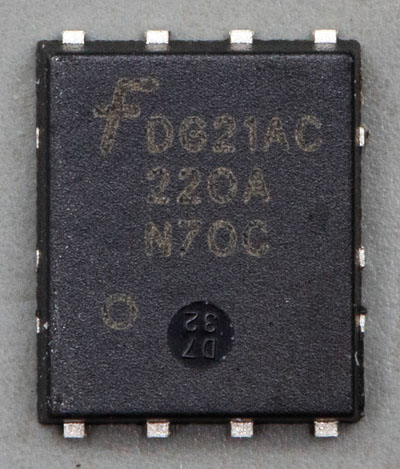
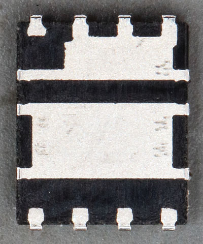

Now let us take a look into a more up to date transistor! The Fairchild FDMS3602S offers two asymmetric n-channel MOSFETs in a low-profile Power 56 package. The design is optimized for a buck converter. Transistor Q1 is the switching transistor. Q2 is the active rectifier. The integration in a package allows us to keep the traces short that carry switched currents. That reduces losses due to parasitic inductances and EMC problems.
The transistors own significantly different specs. Breakdown voltage is 25 for both transistors. Q1 offers a maximum on resistance of 8.1mΩ. The resistance of Q2 is significantly smaller with a maximum of 3.4mΩ. This is advantageous when the input voltage of a buck regulator is more than twice the output voltage. In this case, Q2 conducts current longer than Q1 and contributes more to the total loss. The datasheet states a permanent current carrying capability of 30A/40A (Q1/Q2, Tc=25°C). Up to 40A/100A are allowed for a short time.
The switching transistor Q1 has a higher impedance, but offers lower capacitances and faster switching. The rise and fall times are typically half those of Q2. This reduces switching losses in Q1 which is loaded with the input voltage.
As being the active rectifier Q2 has a Schottky diode connected in parallel to the intrinsic body diode. The lower forward voltage and smaller reverse capacitance reduce losses in the dead times when both transistors are blocked and in the transition phases. One could use the Schottky diode without driving the transistor. However the datasheet points out that typically for a Schottky diode the reverse current increases sharply with temperature. That can cause problems with the maximum power dissipation of the package. The Schottky diode is not a discrete element, but is located within the PowerTrench MOSFET. Fairchild calls these components SyncFETs.
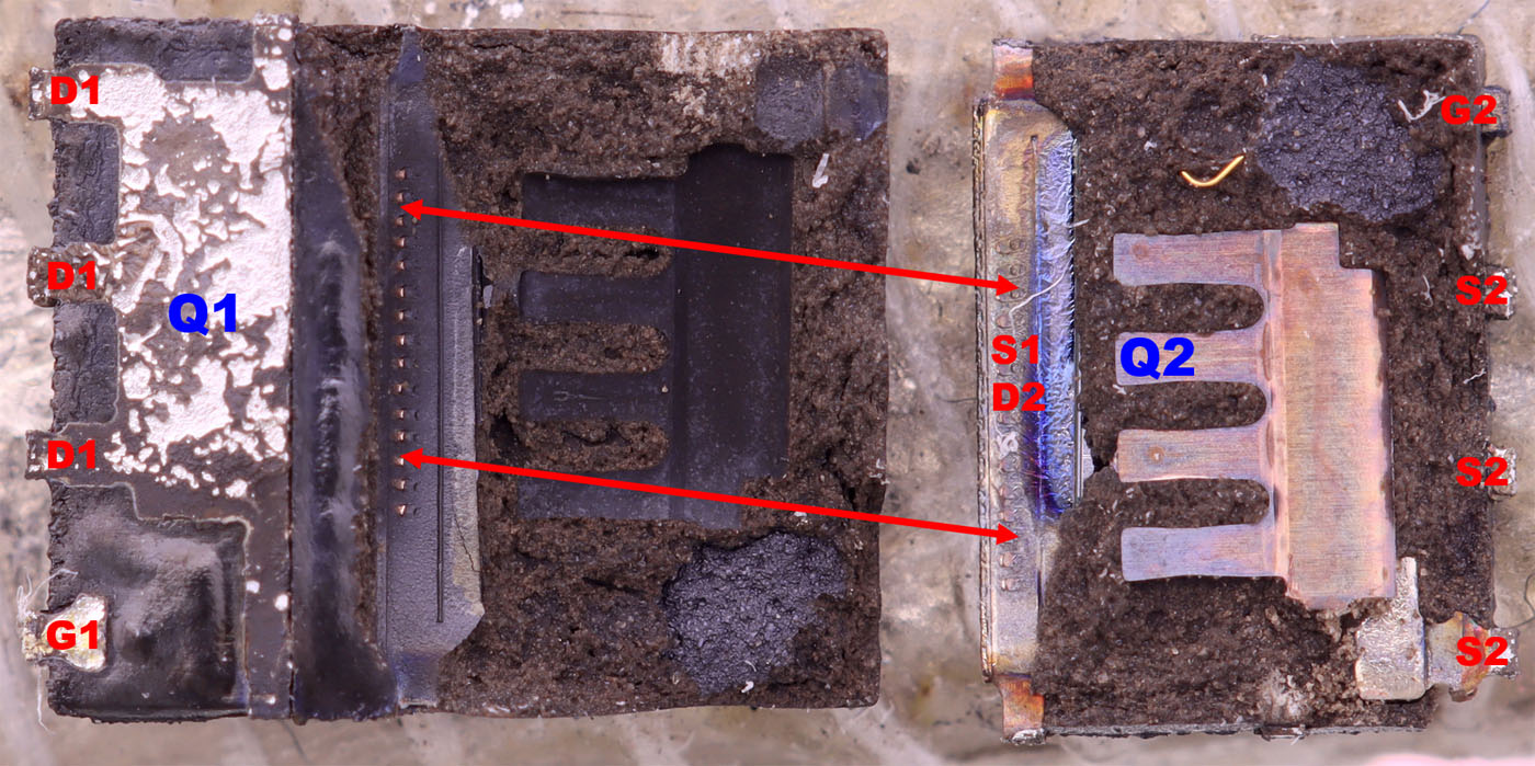
The transistor Q1 is located on the left leadframe. 15 bondwires connect the top of the transistor (source) with the leadframe in the middle. Q2 is placed here. Source of Q2 is connected with a comb-like sheet metal element. Above this contact sheet you can see the bondwire which connects the gate.
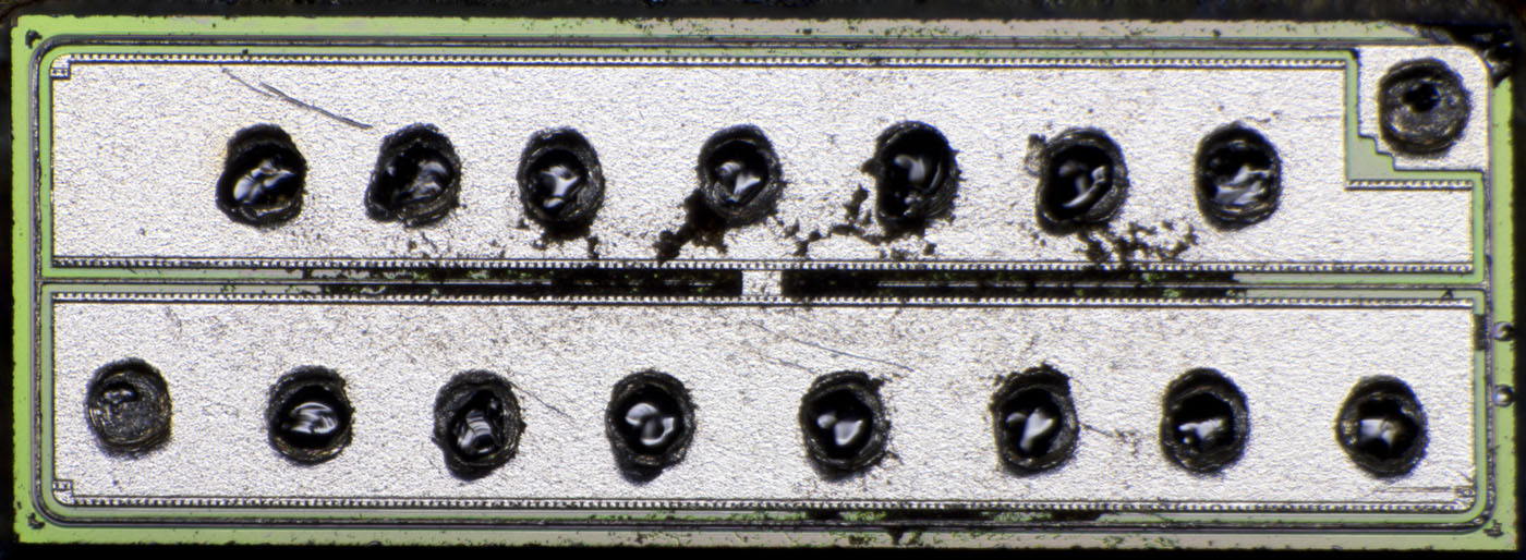
Q1 is 2.1mm x 0.8mm. The source metal layer is divided into two areas.
Vias are visible just at the upper and lower edges of these areas. Most likely the MOSFET consists of many small MOSFET cells as it is common for power MOSFETs (see for example BUK446:
https://www.richis-lab.de/FET07.htm). It is interesting that vias can just be seen on the sides.
The gate potential arrives in the upper right corner and is distributed over the die with a thin frame structure.
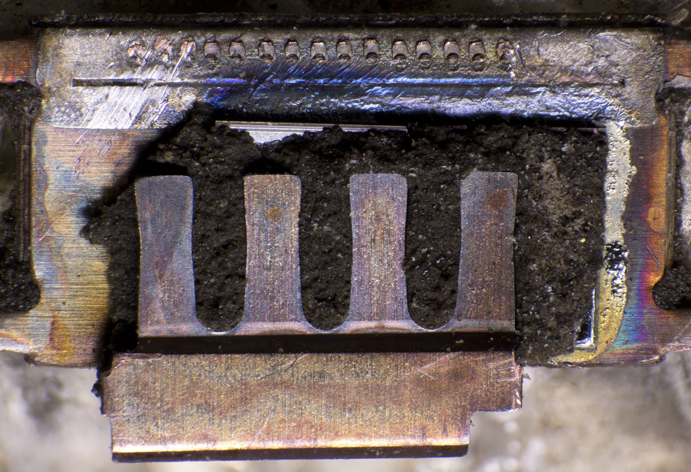
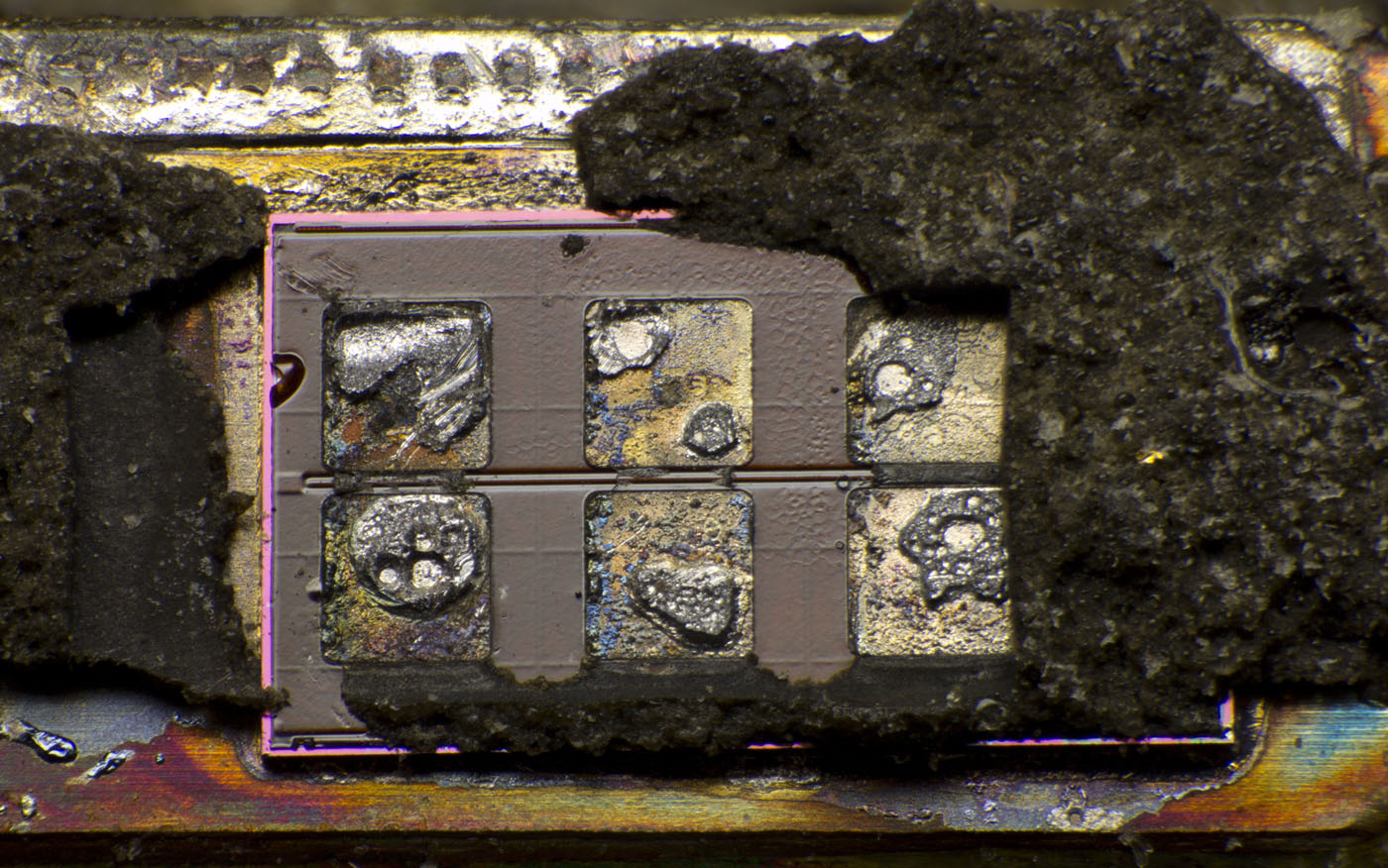
Q2 is 2.5mm x 1.5mm. The contact plate has four contact fingers but just three of them are connected to the die. Apparently this contact element is suitable for contacting wider MOSFETs.
The surface is covered with a protective layer, probably a polyimid. In the middle, at the upper and lower edge thin gate traces can be seen.
https://www.richis-lab.de/FET22.htm 