Author Topic: Transistors - die pictures  (Read 257063 times)

0 Members and 4 Guests are viewing this topic.

Online NoopyTopic starter

  • Super Contributor
  • ***
  • Posts: 1895
  • Country: de
    • Richis-Lab
Re: Transistors - die pictures
« Reply #275 on: December 20, 2020, 08:33:36 pm »
Hey, a glowing J-FET is missing!  ;D
Of course I had to change that:


Breakdown voltage is 45V (D&S -> G). Current is 30mA.


There is a light above and below of every gate electrode. One of the light strips of every gate electrode is mostly covered by the metal electrodes which are not perfectly aligned.


https://richis-lab.de/FET06.htm

 :-/O
 
The following users thanked this post: RoGeorge

Online NoopyTopic starter

  • Super Contributor
  • ***
  • Posts: 1895
  • Country: de
    • Richis-Lab
Re: Transistors - die pictures
« Reply #276 on: December 24, 2020, 04:49:01 am »
More power!  :box:


BUK446, a Power-MOSFET which can handle 800V (BUK446-800) or 1000V (BUK446-1000).
The B at the end makes it possible to conduct 1,5A (A gives you 1,7A). Peak current is 6A (6,8A).


The die is quite big for a TO220-package: 4,6mm x 4,5mm.


A lot of small MOSFETs as we know it.


They left the corners blank to reduce electrical stress. Sharp edges give you a high electrial field strenght which can lead to partial discharge and breakdown.
Around the active area there are potential steering rings for a smooth electrical field.  :-/O


https://www.richis-lab.de/FET07.htm

 :-+
 
The following users thanked this post: exe, SilverSolder, Miyuki

Online NoopyTopic starter

  • Super Contributor
  • ***
  • Posts: 1895
  • Country: de
    • Richis-Lab
Re: Transistors - die pictures
« Reply #277 on: December 26, 2020, 05:46:30 am »


Tesla KU605


In the package glued on the lid is a white cylinder. The cylinder probably absorbs humidity.


Still the die is potted with some red silicone.
Tesla used ribbon bonds. Interesting.


You can see the MESA-edge.
Tesla has put solder on the side of the die. I haven´t seen that in other power transistors.  :-//


The ribbon bond contact looks quite interesting.


And of course it glows!  ;D
7,5V / 1A


https://www.richis-lab.de/Bipolar31.htm

 :-/O
 
The following users thanked this post: BravoV, SilverSolder, RoGeorge, Miyuki

Offline BravoV

  • Super Contributor
  • ***
  • Posts: 7549
  • Country: 00
  • +++ ATH1
Re: Transistors - die pictures
« Reply #278 on: December 26, 2020, 06:43:36 am »
Great works and photos as usual, thank you.  :clap:  :-+

Still the die is potted with some red silicone.

What did you use or how did you clean the red silicone ? Using solvent ? Or else ?

Online NoopyTopic starter

  • Super Contributor
  • ***
  • Posts: 1895
  • Country: de
    • Richis-Lab
Re: Transistors - die pictures
« Reply #279 on: December 26, 2020, 07:03:51 am »
Thanks!  :)

You can peel away the red coating using tweezers, mostly in quite big parts. Thankfully it doesn't stick too hard and the ribbon bonds are quite robust.
The small remains didn't bother me.

Offline SilverSolder

  • Super Contributor
  • ***
  • Posts: 6126
  • Country: 00
Re: Transistors - die pictures
« Reply #280 on: December 26, 2020, 04:08:04 pm »

Those ribbons do look a lot more solid than the thin bond wires we normally see.  Wonder if they give any real advantages?
 

Online NoopyTopic starter

  • Super Contributor
  • ***
  • Posts: 1895
  • Country: de
    • Richis-Lab
Re: Transistors - die pictures
« Reply #281 on: December 26, 2020, 04:29:44 pm »
I assume back in these days every company had it's own special way of construction. Not everything was optimized to that extend it is today. These ribbon bonds have a pretty low resistance. But I'm afraid bonding such big metal work without damaging the die was not a easy task... :-/O

Offline BravoV

  • Super Contributor
  • ***
  • Posts: 7549
  • Country: 00
  • +++ ATH1
Re: Transistors - die pictures
« Reply #282 on: December 26, 2020, 04:32:04 pm »
And probably lower yield too compared to bond wires ?  :-//

Online NoopyTopic starter

  • Super Contributor
  • ***
  • Posts: 1895
  • Country: de
    • Richis-Lab
Re: Transistors - die pictures
« Reply #283 on: December 26, 2020, 04:38:01 pm »
Perhaps they wanted to keep the inductance low too.
OK, it´s a quite old and bulky part but after all it´s a switching transistor with a fg of at least 5MHz...

Online NoopyTopic starter

  • Super Contributor
  • ***
  • Posts: 1895
  • Country: de
    • Richis-Lab
Re: Transistors - die pictures
« Reply #284 on: December 26, 2020, 11:01:32 pm »

Let´s look inside a KU607 to compare it with the KU605:


210V vs. 200V
hFE and Ic are the same
70W vs. 50W
>9MHz vs. >5MHz
=> a little bit better than the KU605


Nothing special inside but there is no humidity absorber in this package.


Hey, the die area is the same as in the KU605 and also the structures look the same!
It seems Tesla has optimized the internal structures/doping...


https://www.richis-lab.de/Bipolar32.htm

 :-/O

Online NoopyTopic starter

  • Super Contributor
  • ***
  • Posts: 1895
  • Country: de
    • Richis-Lab
Re: Transistors - die pictures
« Reply #285 on: December 28, 2020, 04:36:04 am »


KU608
Uce: 250V, 40V more than the KU607.


In the package I found an absorber like in the KU605 but with a different shape. In the KU607 there was no absorber. Strange...  :-//


Looks familiar...


But the die is slightly smaller (5,6mm x 5,7mm) than the die of the KU605 and the KU607 (5,8mm x 6,0mm).
It seems Tesla was able to optimize it´s transistor design...


C-E-short...  :-BROKE


https://www.richis-lab.de/Bipolar33.htm

 :-/O

Online NoopyTopic starter

  • Super Contributor
  • ***
  • Posts: 1895
  • Country: de
    • Richis-Lab
Re: Transistors - die pictures
« Reply #286 on: January 04, 2021, 05:42:38 am »


Siliconix IRF640: 200V / 0,18 \$\Omega\$ / 18A / 72Ap


Quite a big die for a TO220-package: 5,8mm x 4,3mm  8)
Three metal lines are conducting the gate potential into the active area.


A lot of tiny MOSFETs.  ;D


In contrast to the high voltage MOSFET BUK446-1000B (https://richis-lab.de/FET07.htm) in the IRF640 the small transistors can also be found in the corners. Lower voltages => lower electrical field strength => less problems   ;D


https://richis-lab.de/FET08.htm

 :-/O
 
The following users thanked this post: RoGeorge

Offline David Hess

  • Super Contributor
  • ***
  • Posts: 17194
  • Country: us
  • DavidH
Re: Transistors - die pictures
« Reply #287 on: January 04, 2021, 11:03:49 am »
Quite a big die for a TO220-package: 5,8mm x 4,3mm  8)

Power MOSFETs brought on development of TO-220 packages which could hold larger dies, and eventually larger TO-220 style packages.  Later TO-220 packages had a lead frame which barely fit within the encapsulation.  Current became so high that separate bond wires to the drain were replaced with a single strip of copper.

I always wanted more powerful bipolar transistors in those enhanced TO-220 packages but if they existed, I never saw them.

Quote
A lot of tiny MOSFETs.

Since the manufacturer is Siliconix, that makes it MOSPOWER!

https://archive.org/details/bitsavers_siliconixdixMOSPOWERApplications_38092918

An International Rectifier part would be a HEXFET with a hexagonal arrangement of cells.  Do they still make these?  I blew up enough of them.
« Last Edit: January 04, 2021, 11:06:35 am by David Hess »
 
The following users thanked this post: Noopy

Online NoopyTopic starter

  • Super Contributor
  • ***
  • Posts: 1895
  • Country: de
    • Richis-Lab
Re: Transistors - die pictures
« Reply #288 on: January 04, 2021, 12:21:38 pm »
Power MOSFETs brought on development of TO-220 packages which could hold larger dies, and eventually larger TO-220 style packages.  Later TO-220 packages had a lead frame which barely fit within the encapsulation.

 :-+


Since the manufacturer is Siliconix, that makes it MOSPOWER!

https://archive.org/details/bitsavers_siliconixdixMOSPOWERApplications_38092918

Thanks for the link, that´s quite an interesting book!


An International Rectifier part would be a HEXFET with a hexagonal arrangement of cells.  Do they still make these?  I blew up enough of them.

I can´t answer that...  :-//

Offline SK_Caterpilar_SK

  • Regular Contributor
  • *
  • Posts: 137
  • Country: sk
Re: Transistors - die pictures
« Reply #289 on: January 04, 2021, 09:24:46 pm »
Man I love this place its absolutely great to just gaze at lighting up transistors. But really? KD501 at 1A? Those things can to 10A continues safely ! you should really try them on a heatsink low voltage low disspation high current lets go light the entire room up. I thought the inside of the TO3s were dark cold places, indeed wrong lit by the current :D I like it.

If you ever come across a tesla germanium transistor such as 7NU74 73 or 6NU Take a look at those. I have milled one 6NU74 (because some sadistic murderer broke its legs off) and it turned out to be a metal capsule in which the semiconducotr was located. The metal "can" was split in 3 parts acting as electrodes I guess. Oh and It also had a rattly absorband inside. I rock a pair of 7NU74s in a AB amp and they are very interesting :)
 

Offline jananetha

  • Newbie
  • Posts: 2
  • Country: in
Re: Transistors - die pictures
« Reply #290 on: January 05, 2021, 08:31:11 am »
can you share video link
 

Online NoopyTopic starter

  • Super Contributor
  • ***
  • Posts: 1895
  • Country: de
    • Richis-Lab
Re: Transistors - die pictures
« Reply #291 on: January 05, 2021, 08:46:53 am »
But really? KD501 at 1A? Those things can to 10A continues safely !

But not over their base-emitter-junction and even less when "working" in breakdown!  :D


I thought the inside of the TO3s were dark cold places, indeed wrong lit by the current :D I like it.

There is quite some light in some semiconductors!   8) Sometimes even in normal operation! More coming soon... ;D


If you ever come across a tesla germanium transistor such as 7NU74 73 or 6NU Take a look at those. I have milled one 6NU74 (because some sadistic murderer broke its legs off) and it turned out to be a metal capsule in which the semiconducotr was located. The metal "can" was split in 3 parts acting as electrodes I guess. Oh and It also had a rattly absorband inside. I rock a pair of 7NU74s in a AB amp and they are very interesting :)

Sounds like this one:
https://richis-lab.de/Bipolar27.htm


can you share video link

Which video link?  :-//


Online NoopyTopic starter

  • Super Contributor
  • ***
  • Posts: 1895
  • Country: de
    • Richis-Lab
Re: Transistors - die pictures
« Reply #292 on: January 05, 2021, 08:51:02 pm »


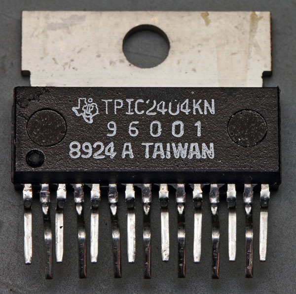
TPIC2404: four 1A-Smart-Transistors with overvoltage protection, overcurrent protection, freewheeling diodes to an external potential, enable input and error output.
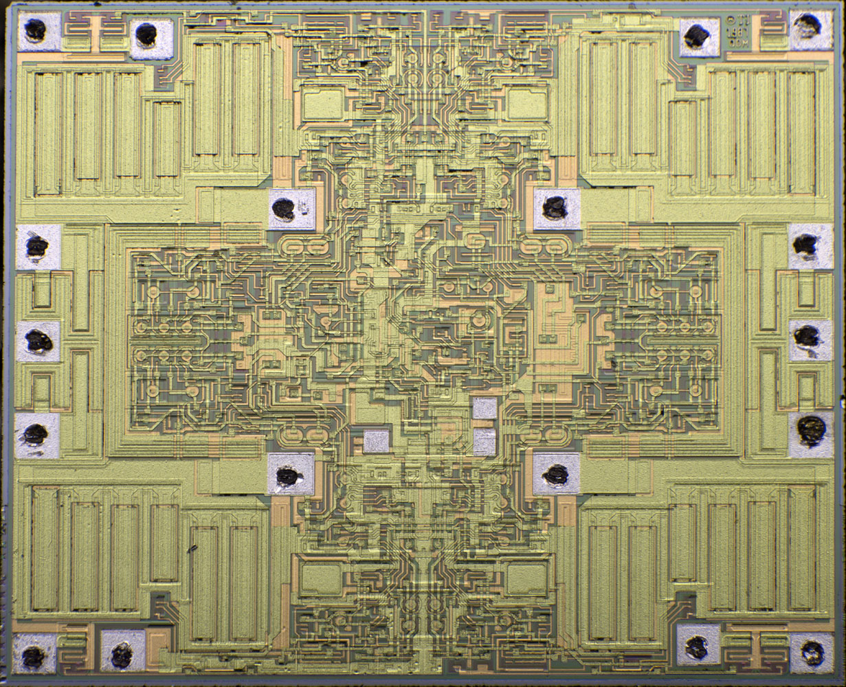


The die is 3,9mm x 3,4mm and uses two metal layers.
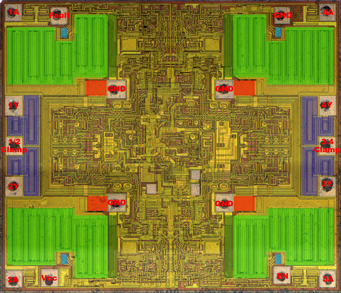


You can identify a lot of parts of the TPIC2404:
Green: Output transistor
Dark green: Output transistor driver
Dark blue: Freewheeling / Clamping diodes.
Red: Shunt for overcurrent protection
Blue: Overtemperature protection
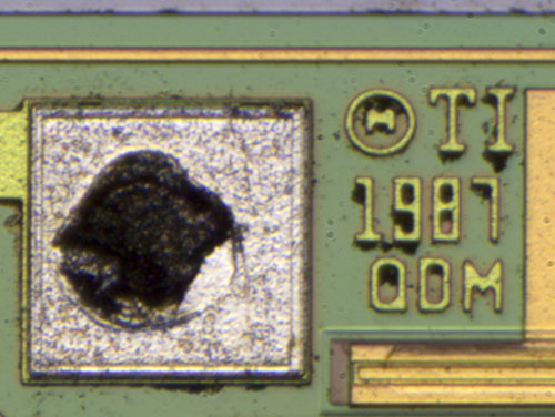


1987
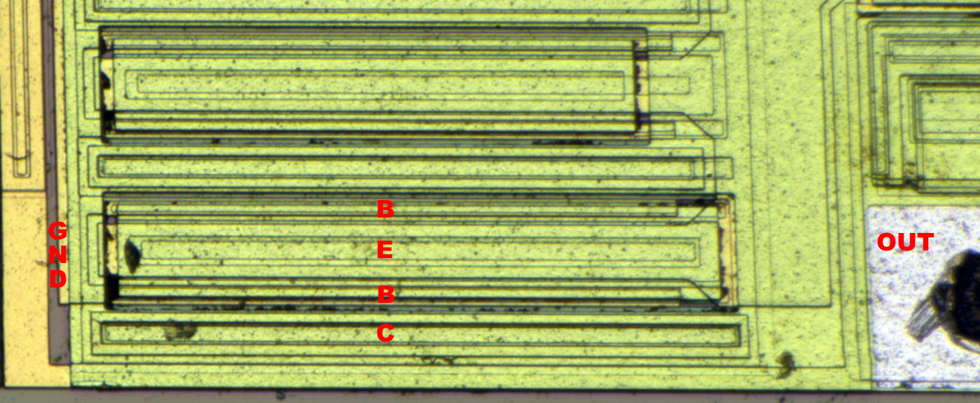


The parts of the output transistor are hard to identify because of the two metal layers.
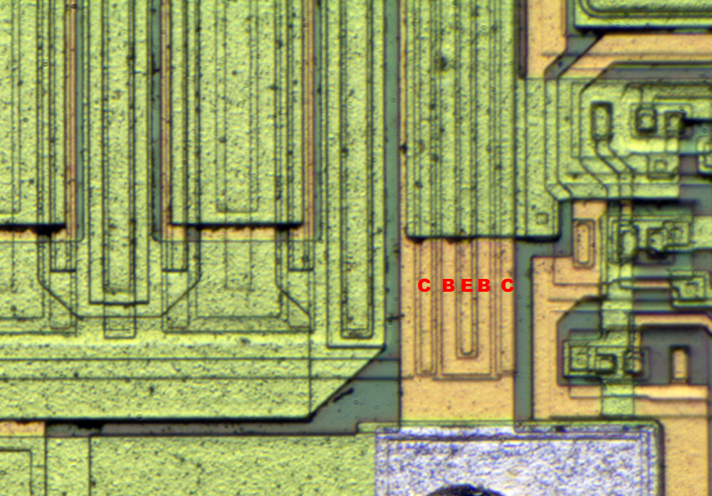


Same with the driver transistor.
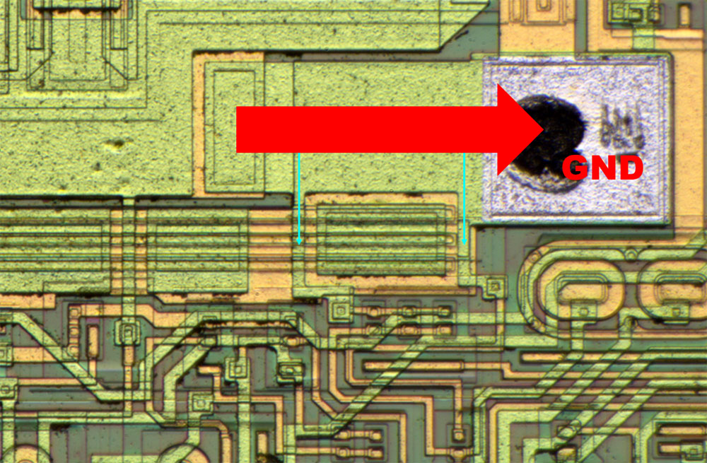


Shunt-Current-Measurement
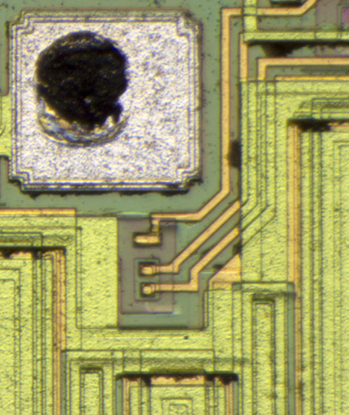


Temperature sensor
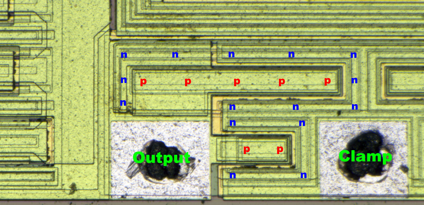


Freewheeling / Clamping diode
It uses the two metal layers in parallel to get a low resistance in this small area.
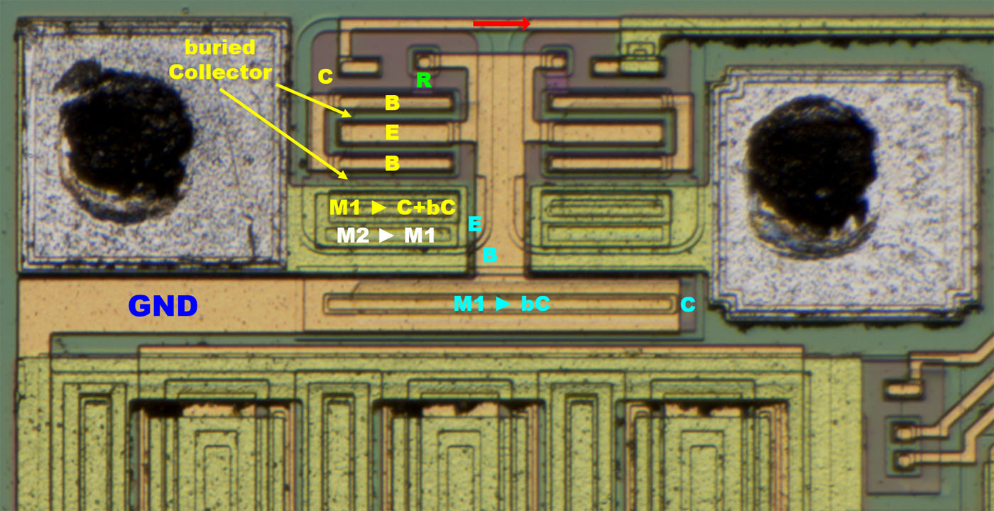
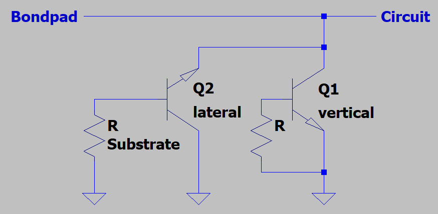


The input protection has a transistor at the bondpad with base and emitter connected (red). Base-collector gives you a diode with a high breakdown voltages and protects the circuit against negative voltages.
In the collector area there is a MOSFET which can switch to ground (black). The green resistor is a pull-down for the gate. Via a small capacitor (yellow) a voltage surge activates the MOSFET and is shunted to ground.  :-+


https://www.richis-lab.de/Bipolar30.htm

 :-/O
 
The following users thanked this post: exe, Rod

Online NoopyTopic starter

  • Super Contributor
  • ***
  • Posts: 1895
  • Country: de
    • Richis-Lab
Re: Transistors - die pictures
« Reply #293 on: January 07, 2021, 07:46:55 pm »


A little cursty.  :o It´s a Siemens AD133(-V), a Ge-PNP-Transistor: 32V, 15A, hfe 50-100 ("V" is the bin with the best hfe).


Pins with soldering eyelets  :-+
There is also a pin for the collector connection.  :-+


There is a white drying agent in the package and a black potting on the transistor.


IPA removes the black potting.


As seen in the 2N3055 (https://www.richis-lab.de/2N3055_01.htm) and the AD148 (https://www.richis-lab.de/Bipolar27.htm) Siemens used a single metal plate which is soldered into the package and then has been fused.


The die diameter is 4,4mm, only a little bit bigger than the diameter of the AD148 die (4,1mm).


https://www.richis-lab.de/Bipolar34.htm


Offline exe

  • Supporter
  • ****
  • Posts: 2622
  • Country: nl
  • self-educated hobbyist
Re: Transistors - die pictures
« Reply #294 on: January 07, 2021, 08:20:31 pm »
How much did the transistors cost back in the day? Say, in 60-x, 70-x, and 80-x. I assume in 90-x they were affordable. I also heard PNP transistors were more expensive than NPN.
 

Online NoopyTopic starter

  • Super Contributor
  • ***
  • Posts: 1895
  • Country: de
    • Richis-Lab
Re: Transistors - die pictures
« Reply #295 on: January 07, 2021, 08:28:05 pm »
How much did the transistors cost back in the day?

I don´t know that, would have to do some research.  :-//
But I´m sure one of the people reading this knows what you would have to pay back in the days.


I also heard PNP transistors were more expensive than NPN.

I´m pretty sure that´s wrong for Ge-transistors. PNP-transistors were easier to build. Not every manufacturer was even able to built npn power transistors.  :-/O

Online NoopyTopic starter

  • Super Contributor
  • ***
  • Posts: 1895
  • Country: de
    • Richis-Lab
Re: Transistors - die pictures
« Reply #296 on: January 11, 2021, 06:20:32 pm »


SMY51, a dual-pMOS built 1973 by Funkwerk Erfurt.


The die contains two zener to protect the gate.


On the die there is some gel potting.


You can see the comb-shaped drain and source. On top of drain and source there is the gate electrode. Under the transistors there are the z-diodes connecting the gates to the substrate.


https://www.richis-lab.de/FET09.htm

 :-/O
 
The following users thanked this post: serg-el

Online NoopyTopic starter

  • Super Contributor
  • ***
  • Posts: 1895
  • Country: de
    • Richis-Lab
Re: Transistors - die pictures
« Reply #297 on: January 15, 2021, 08:25:08 pm »
FERD diode please...

I have a FRED in stock.

But right now I can show you a IGBT with a "HEXFRED".


International Rectifier IRG4PH40K // 1200V // 30A continuous @25°C // 60A peak


I had a second one. The marking looked quite strange but it seems to be a genuine part because it has the same dies as the first one.


Interesting, the gate potential distribution lines are not symmetrical.
The die is 6,2mm x 4,3mm. It´s smaller than the die of the IXYS IXGH48N60C3D1 (7,2mm x 6,1mm / https://www.richis-lab.de/Bipolar26.htm) because it has to conduct less current. The IRG4PH40K has a bigger field control area because of the much higher voltage rating.
The brownish coating seems to be a protective layer.


Gate potential distribution over the silicon.


The field control looks interesting. In the corners the metal lines are a little wider and there is a via connecting the silicon underneath.
While most of the field control is coated the first two isolation gaps are left blank.


The marking on the die is mirror inverted. => 1997


And that´s the HEXFRED (4,0mm x 3,0mm).


Field control like on the IGBT.
In the active area there is a honeycomb structure.


https://www.richis-lab.de/Bipolar35.htm


 :-/O
 
The following users thanked this post: exe, RoGeorge, capt bullshot

Offline exe

  • Supporter
  • ****
  • Posts: 2622
  • Country: nl
  • self-educated hobbyist
Re: Transistors - die pictures
« Reply #298 on: January 15, 2021, 09:31:56 pm »
I have a FRED in stock.

You mean FERD, right? I'm in great anticipation! There is very little info on these beasts.

While searching for info, it seems there a newer generation called cc-ferd: https://www.semanticscholar.org/paper/A-New-Generation-of-Power-Diode%3A-Charge-Coupled-Lee-Ngwan/724f82fd90cbea5b81bb116e646b7105117ca701 . I'm trying to find a full paper. Although, looking at research papers, there seems to be many ideas, but few make into silicon.

UP: found pdf scholar.google.com
« Last Edit: January 15, 2021, 09:41:33 pm by exe »
 

Online NoopyTopic starter

  • Super Contributor
  • ***
  • Posts: 1895
  • Country: de
    • Richis-Lab
Re: Transistors - die pictures
« Reply #299 on: January 16, 2021, 04:17:48 am »
I have a FRED in stock.

You mean FERD, right? I'm in great anticipation! There is very little info on these beasts.

While searching for info, it seems there a newer generation called cc-ferd: https://www.semanticscholar.org/paper/A-New-Generation-of-Power-Diode%3A-Charge-Coupled-Lee-Ngwan/724f82fd90cbea5b81bb116e646b7105117ca701 . I'm trying to find a full paper. Although, looking at research papers, there seems to be many ideas, but few make into silicon.

UP: found pdf scholar.google.com

FRED, FERD,... ;D
Yes, I wanted to write FERD: https://www.mouser.de/ProductDetail/STMicroelectronics/FERD40H100SFP/?qs=ZSypp649SOX1Ct15PSJtkQ%3D%3D
CC-FERD, interesting...
 
The following users thanked this post: exe


Share me

Digg  Facebook  SlashDot  Delicious  Technorati  Twitter  Google  Yahoo
Smf