Author Topic: QFN footprint, soldermask between pads of 0.5 pitch or not  (Read 5614 times)

0 Members and 1 Guest are viewing this topic.

Offline mjkuwpTopic starter

  • Supporter
  • ****
  • Posts: 260
  • Country: us
  • mechanical engineering defector
    • The Mz Lab
QFN footprint, soldermask between pads of 0.5 pitch or not
« on: June 04, 2014, 11:55:07 am »
I have made a few versions of a board with VQFN-28 0.5 pitch footprint.  The footprint has worked out fine although I have had some minor difficulty soldering the part due to my lack of part-placing skills : |

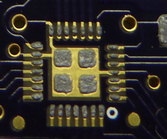
My question is whether the new footprint is OK (soldermask between pads and 3 areas of double-thickness) and if it is better than my old one (large area of soldermask removed).

I am in the USA and OSH Park has made all of my boards and I highly recommend their service.

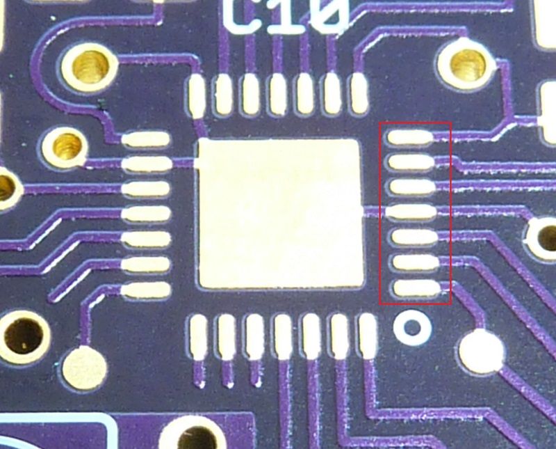
On the most recent production they have done something I have not seen before.  They modified a footprint on my board.  I had been leaving all the pads standing off the board without soldermask between them.  I found this recommendation somewhere.... but have forgotten where it came from.   With this build the board house or OSH Park changed the pattern. 

My biggest question is whether the extra thickness of copper + soldermask is likely to cause a problem in soldering being that it may raise the height of the chip.

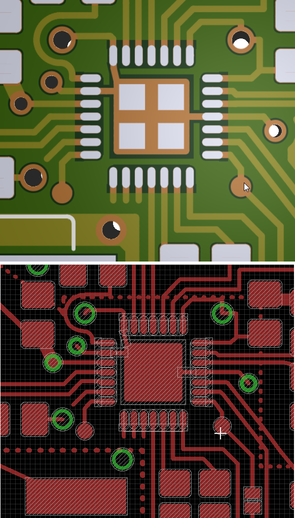
Here is an image of my footprint in Eagle and one from a Gerber Viewer from mayhewlabs.com


Here is an image of part of the very nice board that OSH Park produced.  I made a red rectangle to represent one of the areas I had removed soldermask.
I should say that this board is very high quality, the alignment is really good and the silkscreen is really beautiful.  no complaints at all : )

There are 3 places where pads are connected to the center pad.  This is where analog ground and digital ground meet.  Will the 3 spots where soldermask potentially lifts up the chip cause any trouble?


Below is an image showing an older board - my intended footprint


thanks!
Mark


PS - here is one reference.

http://cache.freescale.com/files/analog/doc/app_note/AN1902.pdf
 

Offline 8086

  • Super Contributor
  • ***
  • Posts: 1085
  • Country: gb
    • Circuitology - Electronics Assembly
Re: QFN footprint, soldermask between pads of 0.5 pitch or not
« Reply #1 on: June 04, 2014, 12:58:13 pm »
It should be fine. I've done plenty like that with no issues.
 

Offline nctnico

  • Super Contributor
  • ***
  • Posts: 27492
  • Country: nl
    • NCT Developments
Re: QFN footprint, soldermask between pads of 0.5 pitch or not
« Reply #2 on: June 05, 2014, 12:53:20 am »
I'd keep soldermask between the pads. Don't make the pad too wide. Narrow pads are less prone to bridging.
There are small lies, big lies and then there is what is on the screen of your oscilloscope.
 

Offline thm_w

  • Super Contributor
  • ***
  • Posts: 6827
  • Country: ca
  • Non-expert
Re: QFN footprint, soldermask between pads of 0.5 pitch or not
« Reply #3 on: June 05, 2014, 01:04:09 am »
I'm very surprised that they would have modified your footprint without asking.
Occasionally I have received some questions when gerber has a clear sign of mistake (in yours those traces going to nowhere might be flagged for example).

I think the new footprint is better than your old one. The extra exposed copped areas on old could leech solder away from the pins.
Profile -> Modify profile -> Look and Layout ->  Don't show users' signatures
 

Offline mjkuwpTopic starter

  • Supporter
  • ****
  • Posts: 260
  • Country: us
  • mechanical engineering defector
    • The Mz Lab
Re: QFN footprint, soldermask between pads of 0.5 pitch or not
« Reply #4 on: June 05, 2014, 01:49:12 am »
...
I think the new footprint is better than your old one. The extra exposed copped areas on old could leech solder away from the pins.

thanks for your thoughts.  I very much believe they had good intentions.  As you say this pattern may be better.  The extra exposed copper was in done by me to prevent shorting between pins - which had happened on an older build.  However, this was only because it was cheaper to re-spin the boards without bothering with a new stencil.  This solved the problem of shorting but the resulting solder joints were not so pretty.

I will be careful with this new build to not let any extra paste under the stencil and to level it off nicely.  hoping for really good results.


Offline mjkuwpTopic starter

  • Supporter
  • ****
  • Posts: 260
  • Country: us
  • mechanical engineering defector
    • The Mz Lab
Re: QFN footprint, soldermask between pads of 0.5 pitch or not
« Reply #5 on: June 11, 2014, 01:33:12 am »
turns out you were all correct! but I didn't really doubt that.  I made up 3 boards over the weekend in my toaster and the 3 ics look nearly perfect with just one short.  It will be easy to patch that up.  With my old footprint I had made functional joints but with this new pattern the joints have nice fillets on them.  The posts above might be a bit confusing.  The main point is that there is soldermask between the pads - an adjustment that OSHPark made to the design I submitted.

I used fresh paste lead solder from Digikey - Chipquik.


The other joints all look like the one above except without shorting.  I guess if anything next time I might just put slightly more pressure on the squeegee when I drag the paste across.

This build is also related to experiments with a tarnished copper sheet as the platen in my oven but that topic is for a different thread.


Share me

Digg  Facebook  SlashDot  Delicious  Technorati  Twitter  Google  Yahoo
Smf