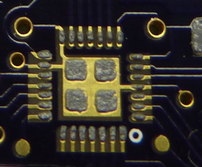
I have made a few versions of a board with VQFN-28 0.5 pitch footprint. The footprint has worked out fine although I have had some minor difficulty soldering the part due to my lack of part-placing skills : |
My question is whether the new footprint is OK (soldermask between pads and 3 areas of double-thickness) and if it is better than my old one (large area of soldermask removed).I am in the USA and OSH Park has made all of my boards and I highly recommend their service.
On the most recent production they have done something I have not seen before. They modified a footprint on my board. I had been leaving all the pads standing off the board without soldermask between them. I found this recommendation somewhere.... but have forgotten where it came from. With this build the board house or OSH Park changed the pattern.
My biggest question is whether the extra thickness of copper + soldermask is likely to cause a problem in soldering being that it may raise the height of the chip.
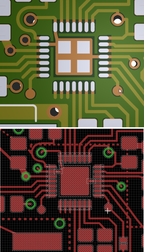
Here is an image of my footprint in Eagle and one from a Gerber Viewer from mayhewlabs.com
Here is an image of part of the very nice board that OSH Park produced. I made a red rectangle to represent one of the areas I had removed soldermask.
I should say that this board is very high quality, the alignment is really good and the silkscreen is really beautiful. no complaints at all : )
There are 3 places where pads are connected to the center pad. This is where analog ground and digital ground meet.
Will the 3 spots where soldermask potentially lifts up the chip cause any trouble?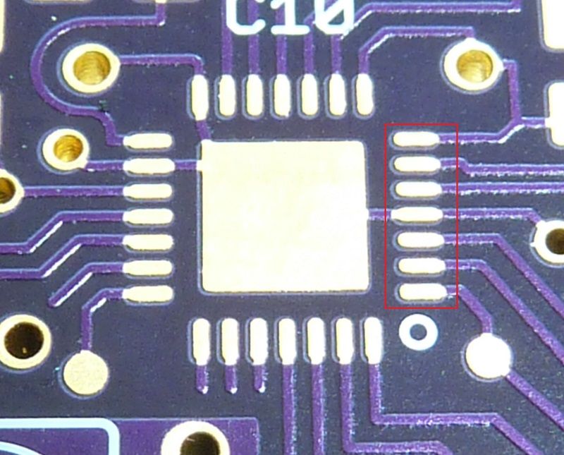
Below is an image showing an older board - my intended footprint
thanks!
Mark
PS - here is one reference.
http://cache.freescale.com/files/analog/doc/app_note/AN1902.pdf


