Part 5. Front End performanceThis part deals with the input stage of the scope, i.e. signal path from the BNC jack on the front panel through to the ADC input. Information presented here may be useful for troubleshooting/repair or learning. There is no design errors fixing in this part.
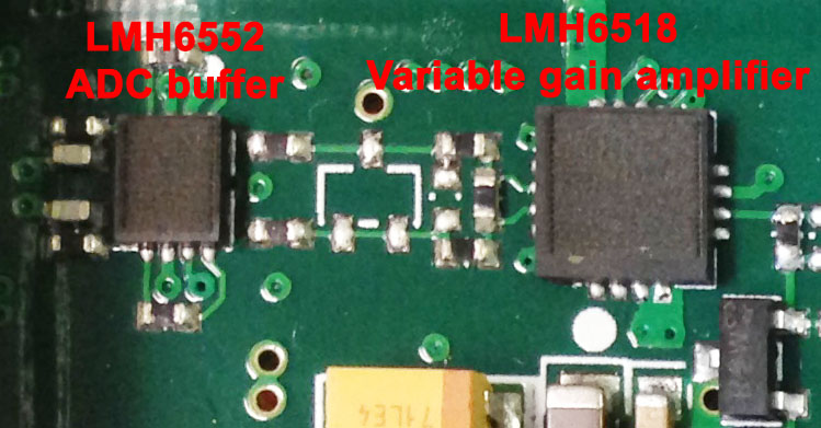
The two scope channels are identical, this is a photo of one channel:
DS2072A_input_stage.jpg

The input BNC jack is at the bottom, together with a relay that connects a 50 Ohm terminating resistor and the resistor itself. The signal travels up through two attenuator stages, passes through a FET transistor buffer, a variable gain amplifier IC with switchable bandwidth in the top part of the photo and exits on the top left via an ADC differential buffer IC. The signal then is routed straight to the ADC input pins.
Same as with the PLL chip, Yaigol made another foolish attempt to disguise the IC part numbers by lasering them off. But EEVBlog is here to uncovers these secrets for you. The VGA with controllable bandwidth is Texas Instruments
LMH6518 900 MHz, Digitally Controlled, Variable Gain Amplifier, and the ADC driver is
LMH6552 1.5-GHz Fully Differential Amplifier from the same company.
Gain_stage.jpg
DS2072A can switch input impedance between 50 Ohm and high impedance. However it also has a stupid bug causing the scope forget it was on 50 Ohm between power ups. You work with an RF circuit, you turn 50 Ohm input On, do you stuff, power off the scope for the night, come back couple days later, power it on, measure your circuit again and ...

the ends do not meet. Perhaps need to turn 50 Ohm termination? You go to settings, hmmm.... it shows 50 Ohm is On

, unless you realize you need to cycle the setting to get 50 Ohm termination back.

The stupid thing tells you it is on 50 Ohm whereas in fact it is not. I have not tested if the bug was fixed in the last firmware. It was not obvious in the earlier firmware either, I could not understand a pattern how/when that happened, it did not happen every time.
The following is a VNA screenshot of input impedance on 50 Ohm setting, Yaigol vs Tektronix 2467B 400MHz analog scope. Yaigol traces are red/green, Tek is blue/yellow. Above 100MHz Tek has a better 50 Ohm compliance.
S11 Yaigol vs Tek.jpg

The following is a VNA screenshot of Yaigol on High Impedance setting. Input impedance is capacitive with Cin about 18.5pF.
S11 Yaigol high impedance.jpg

The attenuator has two stages, a reverse engineered schematic is provided below. I cannot guarantee 100% correctness, I did not try very hard, but it gives you an idea about the overall topology.
DS2072A attenuator.gif
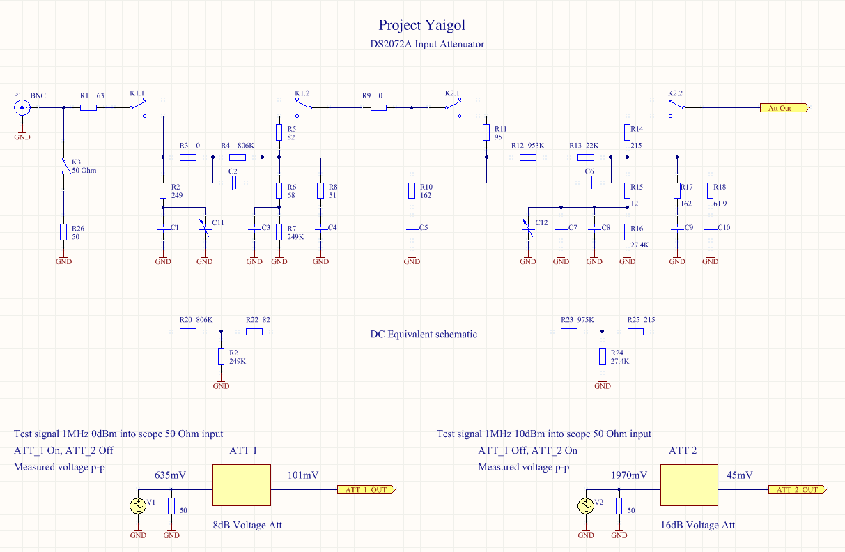
Parts annotation in the schematic is arbitrary. I captured the resistor values but did not measure the capacitors. The topology has quite a few frequency dependent correction circuits but if eliminate them, a equivalent schematic at DC can be composed, which was presented in the above picture.
The first stage appears to have 8dB voltage attenuation, the second stage 16dB, which I calculated based on actual in-circuit measurements of a signal passing through the stages - the test conditions are indicated in the above picture at the bottom.
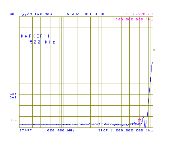
In terms of power the attenuators present 16dB and 32dB attenuation stages, with 48dB of power attenuation when both attenuators are engaged. Interestingly, the overall attenuation of the input stage from input jack to the output of the VGA LMH6518 measured at its output is 32dB. The following VNA screenshot shows attenuation level with both attenuators engaged relative to attenuators turned off. It can be seen that total attenuation of the signal path is about 33dB.
BW limit off with attenuator relative dB.gif
So how come the total loss of the two attenuators is 48dB but we measured only 32dB at VGA output? Apparently the VGA compensates for the missing 16dB loss. This may be kind of stupid, why attenuate and then compensate by amplifying. My guess it is a compromise to have an input stage with wide range of V/Div settings. The VGA chip itself has a variable attenuator and static gain blocks - refer to Fig.57 in the Datasheet. Page 21 of the Datasheet explains how it works together to build a oscilloscope input front-end.
The next stage after the attenuator is DC/AC coupling control circuit (Y214S electronic relay) and the signal splits to AC path via a capacitor and DC path via an IC (that seems to be AD8510) that mixes it with the vertical offset control voltage (bottom part of the following schematic). The composite signal then enters the JFET high impedance buffer. The first stage of the buffer is a JFET N-channel transistor, the second stage is a NPN emitter follower. The buffer topology boils down to two current sink loaded stages shown in the right part of the schematic (you The Art of Electronics aficionados feel free to correct me if I got it wrong).
DS2072A JFET Buffer.gif

The JFET buffer output is wired to the next stage which performs input conditioning magic, i.e. some of amplification/attenuation and the bandwidth control. It is built on TI LMH6518 variable gain amplifier (a link to the datasheet was provided above). This is where your "enhanced" bandwidth lives. It is also the biggest noise generator out of everything else in the analog signal path.
Gain and bandwidth of LMH6518 amplifier is controlled via SPI bus. Gain settings depend on selected V/Div and input attenuator section. The IC provides selectable bandwidth of 20,100,200,350,650,750 and 900 MHz. In Yaigol DS2000 series scopes I guess the first 3 settings are used. So the little beast is capable of some more. I believe this stage also have feeds from the system processor for offset calibration. The amplifier converts single ended input into a differential output and is followed by the ADC buffer amplifier LMH6552 with voltage gain of 2.

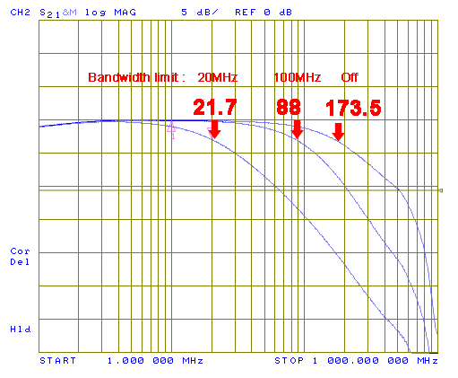
Measured bandwidth at the output of bandwidth controlled LMH6518 is shown next, with the 3 bandwidth settings marked. This is a composite image made from 3 separate measurements with the scope set to 20MHz, 100MHz and Full bandwidth (note we are looking at the hacked scope). The roll-off in the left part of the chart below 3MHz was caused by roll-off of the balun used to take bandwidth measurements and should be ignored.
The 100MHz and Full are not exactly 100MHz and 300MHz, but the ADC driver buffer seems to compensate for it. The following image shows the measured bandwidth of the ADC buffer alone and the combined bandwidth. The overall 3dB bandwidth of the input stage seems to be in the area of 350MHz.

The output of the ADC driver IC goes to the ADC chip via two 47.9 Ohm series resistors.
This completes Part 5 and in Part 6 we will take a look at the ADC.


