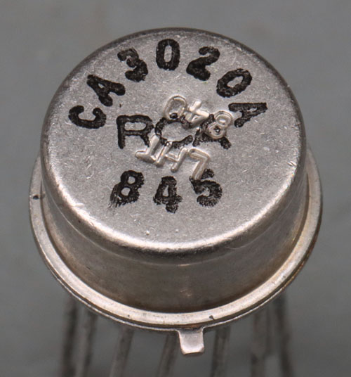
With the CA3020, RCA sold a small power opamp, which was available in two versions. The index A marks the better version, whose output stage can be supplied with up to 12V instead of 9V and can conduct at least 180mA continuously instead of 140mA. This increases the output power from up to 0,5W to a maximum of 1W (10% THD). The bandwidth is typically 8MHz. The permissible operating temperature range is specified as -55°C to 125°C.
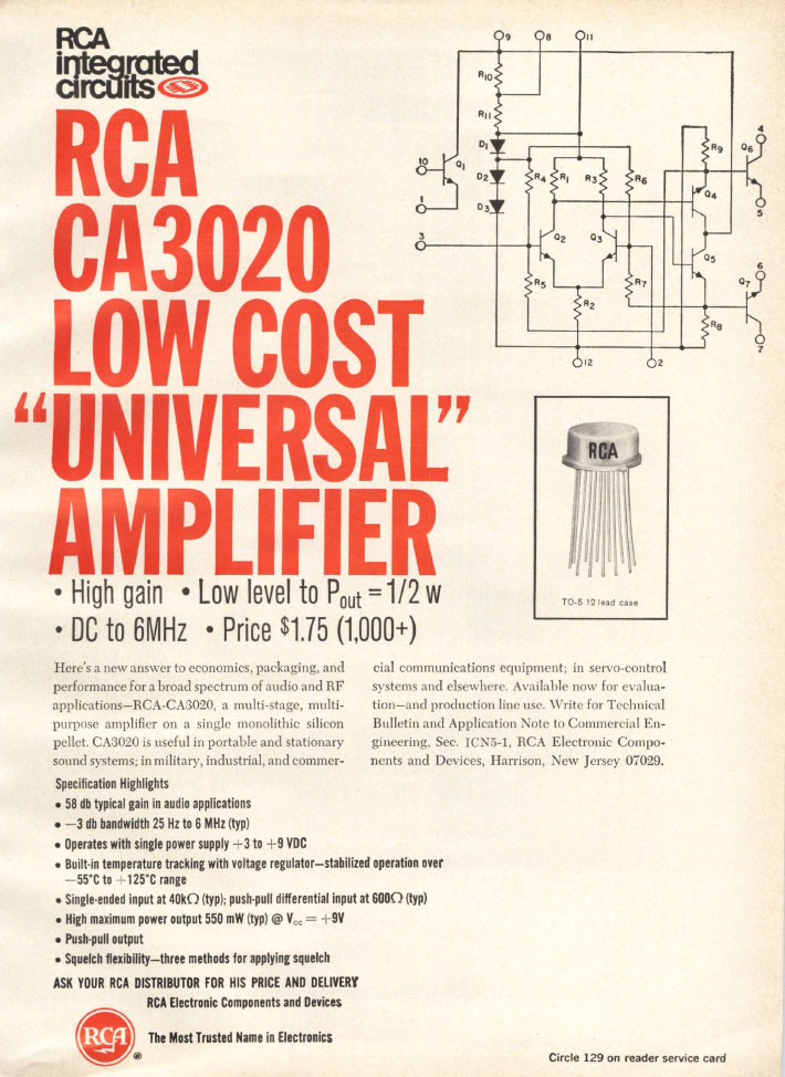
It seems like the A variant has not been sold initially. In this ad in the magazine Electronics from May 1967, there is at least no reference to the A variant.
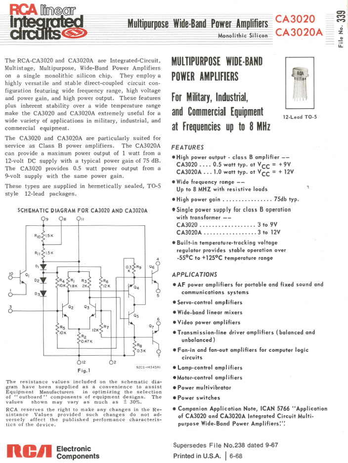
A year later, RCA was already advertising the A version.
Today you can often find the Intersil datasheet for the CA3020. Minor errors have crept in there. Two connections have been omitted and resistor R7 is labelled R5. In the datasheet revision from the year 2000, after 33 years of production, the CA3020 is marked as obsolete.
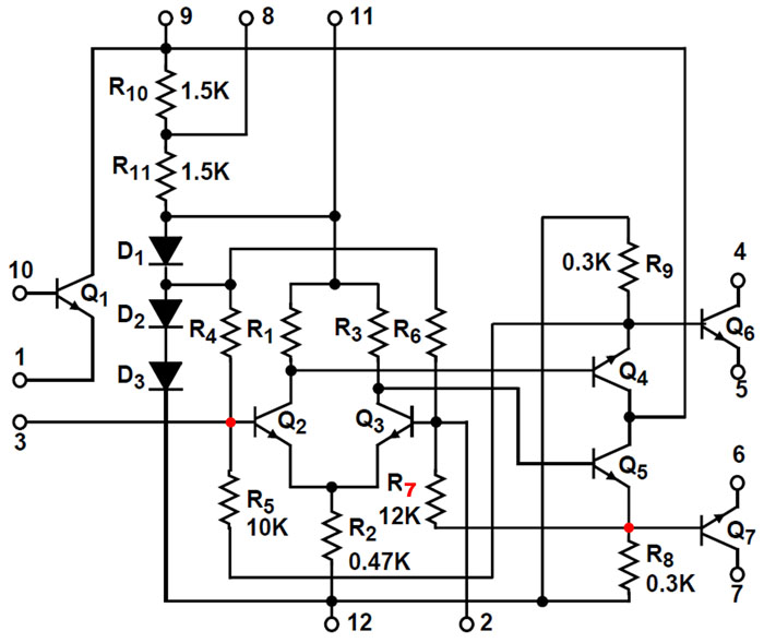
The transistors Q2 and Q3 form a differential amplifier. Transistor Q1 can be used as an upstream buffer stage. The diode chain D1, D2, D3 is used to set the operating point. The voltage from two pn junctions is fed to the inputs of the differential amplifier via R4/R6. The further resistors divide the voltage of the two diodes by slightly more than half. Overall, this generates a certain bias current that is relatively temperature-stable. The potential of the three p-n junctions is applied to the collector resistors R1/R3. While pin 9 is used to supply the circuit, the series resistance of the differential amplifier can be set via pins 8 and 11. A higher resistance reduces the current consumption, but also the output power.
Transistors Q4 and Q5 are driver transistors, from which feedback is fed to the differential amplifier via resistors R5 and R7. The control voltage for the output stage transistors Q6 and Q7 drops out at the emitter resistors R8 and R9. The collector and emitter connections of the output stage transistors are conntected to the pins. One application is driving a load or a transformer with centre tapping. The CA3020 usually works as a class B amplifier. However, it can also be used as a class A amplifier if the potential at the input is raised accordingly.
The resistors in the branches of the differential amplifier are unbalanced in relation to the individual values. This can only be seen here for resistors R5 and R7. The older schematics also note the asymmetry at resistors R1/R3 and R4/R6. However, this also shows that the ratios of the resistors on both sides are not fundamentally different. Why the circuit was not designed completely symmetrical remains an open question.
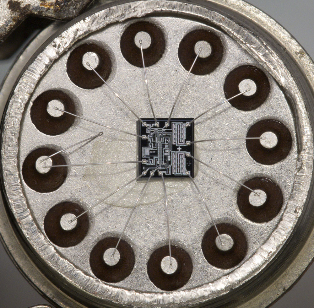
The housing is connected to the reference potential.
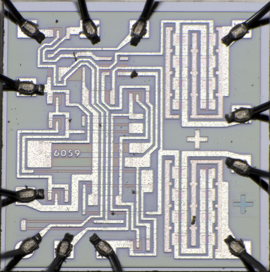
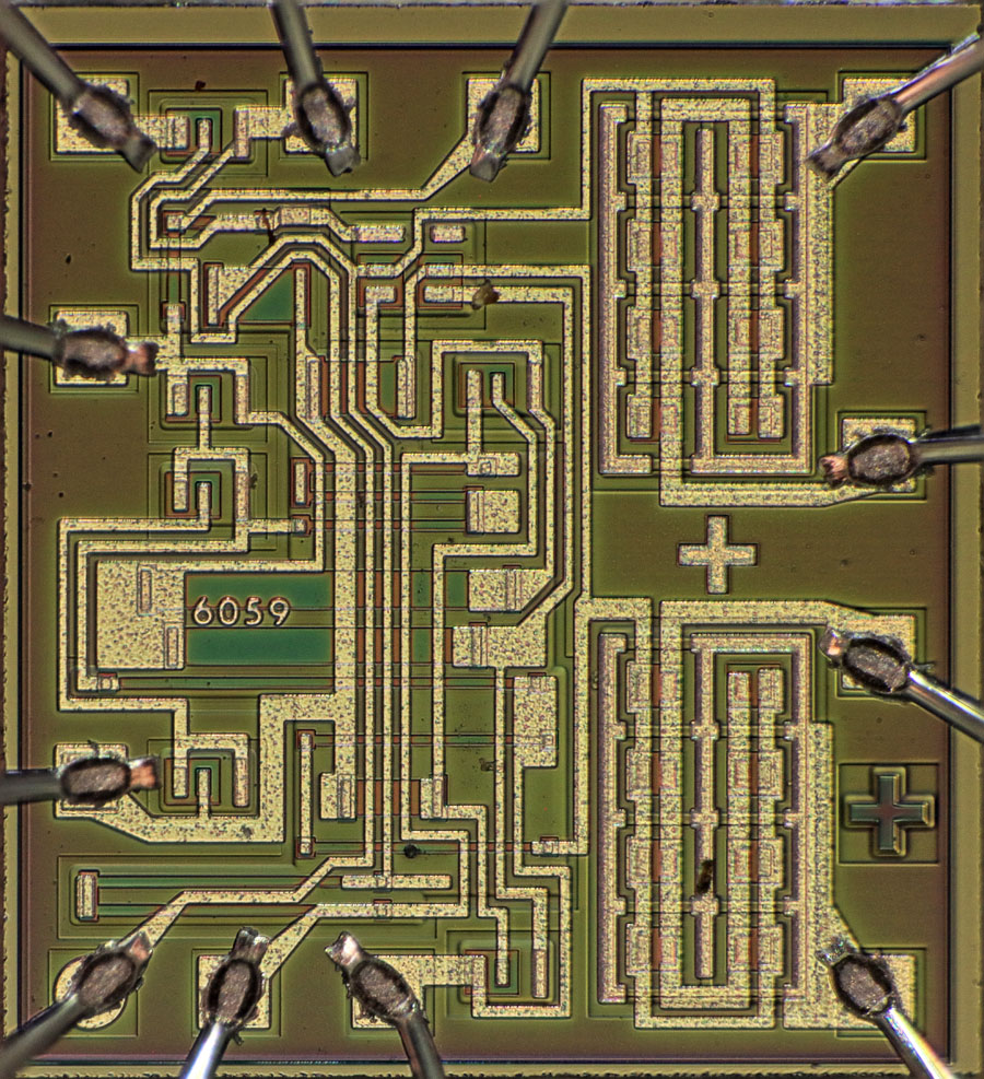
The dimensions of the die are 1,5mm x 1,4mm. 6059 is a typical project designation for RCA. The crosses in the right-hand area are used to check the alignment of the masks to each other.
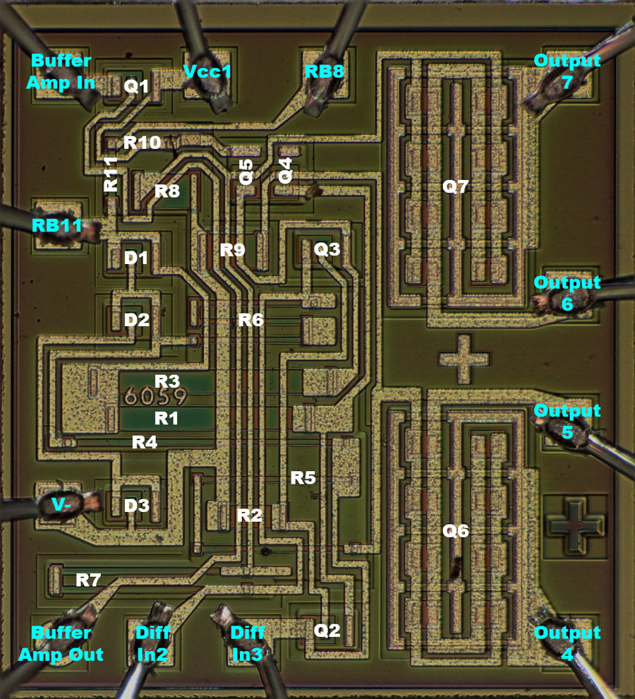
The circuit on the die corresponds to the illustration in the datasheet. Some resistors are constructed in such a way that their contact areas and thus their resistance values can be adjusted more easily. The asymmetry in the differential branches is confirmed.
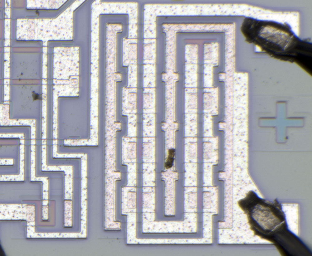
The two large output transistors are located on the right-hand side of the circuit. Each transistor consists of eight small transistors that are directly connected to each other. While the CA3020 is specified for a blocking voltage up to 18V, the CA3020A guarantees a blocking voltage of 25V.
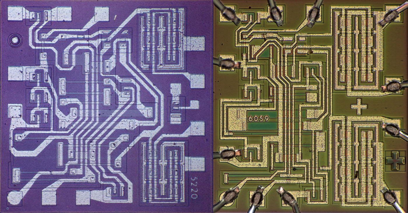
Normally one would assume that the A variant is generated by binning the CA3020. However, this may have been different, at least for the first CA3020 parts. The layout of the CA3020 is illustrated in the magazine Electronics in August 1967. There the project designation is 5220 and the output stage transistors each contain just six individual transistors. The remaining geometries are slightly different, but the circuit is the same.
The different layouts and the fact that the A variant is not mentioned in the first adverts suggest that initially only the lower output power was planned and the circuit was expanded later. Perhaps the power was not sufficient for the planned applications or the designers were initially unsure whether the current distribution would still be sufficiently symmetrical with eight transistors. Perhaps the process has also improved.
https://www.richis-lab.de/Opamp81.htm 


