Author Topic: Opamps - Die pictures  (Read 126314 times)

0 Members and 1 Guest are viewing this topic.

Offline magic

  • Super Contributor
  • ***
  • Posts: 7246
  • Country: pl
Re: Opamps - Die pictures
« Reply #75 on: October 16, 2020, 10:52:40 am »
The point of that is to transfer Q1 current to the Q2 branch of the circuit.

Since Q3 current is constant, it really is not a cascode. Therefore Q1 current has nowhere to go but to R3. This increases/decreases R3 voltage, which is transferred to R4, causing identical increase/decrease in R4 current, which adds to the corresponding opposite change in Q2 current. It's phase summing.

A short way to describe it is that Q3,Q4,Q5 is a resistor-degenerated current mirror biased by two equal collector currents, so in quiescent conditions it simply does nothing besides feeding a current equal to Q5 base current into Q6 base. Then two input stage currents with opposite AC components are fed into the degeneration resistors, resulting in the difference of those currents appearing on Q4 collector.

It's not perfect by the way, because Q4 emitter has nonzero input resistance which to AC currents appears in parallel with R4, so part of the AC current summed at Q4 emitter node escapes through R4 to ground. Depends on the ratio of Q4 intrinsic emitter resistance and R4. R4 can't be too high because if it drops significant voltage, the input transistors will saturate and turn off when their emitters approach ground and likely phase reversal will occur, which this chip is advertised to avoid until some -0.6V. I think the point of this unusual mirror arrangement is to enable operation close to ground and avoid phase reversal below the negative rail.

Current feedback? Dunno. To have feedback, you need to feed something back ;D
What signal is supposed to be fed and from where to where?
« Last Edit: October 16, 2020, 10:56:42 am by magic »
 

Offline magic

  • Super Contributor
  • ***
  • Posts: 7246
  • Country: pl
Re: Opamps - Die pictures
« Reply #76 on: October 16, 2020, 11:08:32 am »
I remember seeing an open loop plot of a certain brand 741 op amp that showed the thermal feedback actually caused the + and - inputs to reverse :o

Of course this would normally be squashed by massive external negative feedback, but still not a good op amp parameter :P

Best,
Sounds very dodgy. No negative feedback won't help, because once the + and - inputs reverse, it becomes positive feedback, which will most likely result in latchup.
I think it meant that polarity of thermal feedback itself was positive, i.e. the output going one way affected offset voltage in such way that the output went even harder the same way, in absence of normal feedback.
I suppose it shows up as increased open loop gain and perhaps some phase oddity at extremely low frequencies.
Honestly, not sure what's wrong with it.
 

Offline capt bullshot

  • Super Contributor
  • ***
  • Posts: 3033
  • Country: de
    • Mostly useless stuff, but nice to have: wunderkis.de
Re: Opamps - Die pictures
« Reply #77 on: October 16, 2020, 12:06:49 pm »
The point of that is to transfer Q1 current to the Q2 branch of the circuit.
...
Current feedback? Dunno. To have feedback, you need to feed something back ;D
What signal is supposed to be fed and from where to where?

Read your explanation and studied the schematic - doesn't match.

So, find my fault (or I might be finding it while writing) ;)

If Q1 collector current increases, Q2 collector current is supposed to decrease as their sum is set by QB10.
Increasing Q1 collector current causes R3 voltage to rise.
Decreasing Q2 collector current causes R4 voltage to decrease.
Q3 emitter voltage rising causes its base voltage rising, as Q3 current is constant. Q4 emitter will follow.
Q4 emitter voltage rising increases R4 current, which is opposite to decreasing Q2 collector current.

OK, I've got it now. It's phase summing because these opposite changes add to the desired Q4 collector voltage output. Thanks.

Looks like the output stage (Q10, driven by Q6 through R5) has significant LF voltage gain, too.
Quite a bunch of tricks to achieve single rail operation (input and output range includes "GND"), not that easy to follow.
Safety devices hinder evolution
 

Offline magic

  • Super Contributor
  • ***
  • Posts: 7246
  • Country: pl
Re: Opamps - Die pictures
« Reply #78 on: October 16, 2020, 04:47:50 pm »
OK, I've got it now. It's phase summing because these opposite changes add to the desired Q4 collector voltage output.
Sorry for the jargon, I've seen it in the Self amplifier book with an implication that it's a common term in opamp literature.
But frankly, I now can't find any example of it on the Internet, so :-//

Anyway, I did indeed mean adding/subtracting the two opposite phase signals from the differential pair.
 

Offline NoopyTopic starter

  • Super Contributor
  • ***
  • Posts: 1903
  • Country: de
    • Richis-Lab
Re: Opamps - Die pictures
« Reply #79 on: October 25, 2020, 10:23:50 pm »
I had started this High-Power-Opamp-thread: https://www.eevblog.com/forum/projects/opa541-high-power-opamp-die-pictures/
Unfortunately there is a OPA541 in the headline and I got some more High-Power-Opamps.  ;D
In future I will post High-Power-Opamps in this thread.


And now welcome the PA-03:
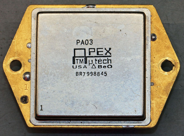


+/-75V, 30A, max. 500W power dissipation and 1MHz cutoff frequency! That´s a power device!  8)


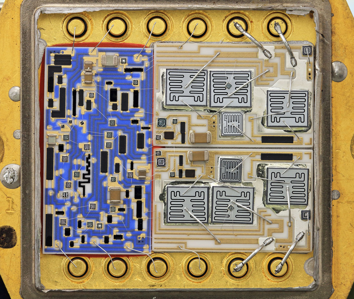
The PA-03 contains three ceramic carrier (beryllium oxide), a highside powerstage, a lowside powerstage and a circuit to control them.
Apex used a lot of different bondwire diameters.
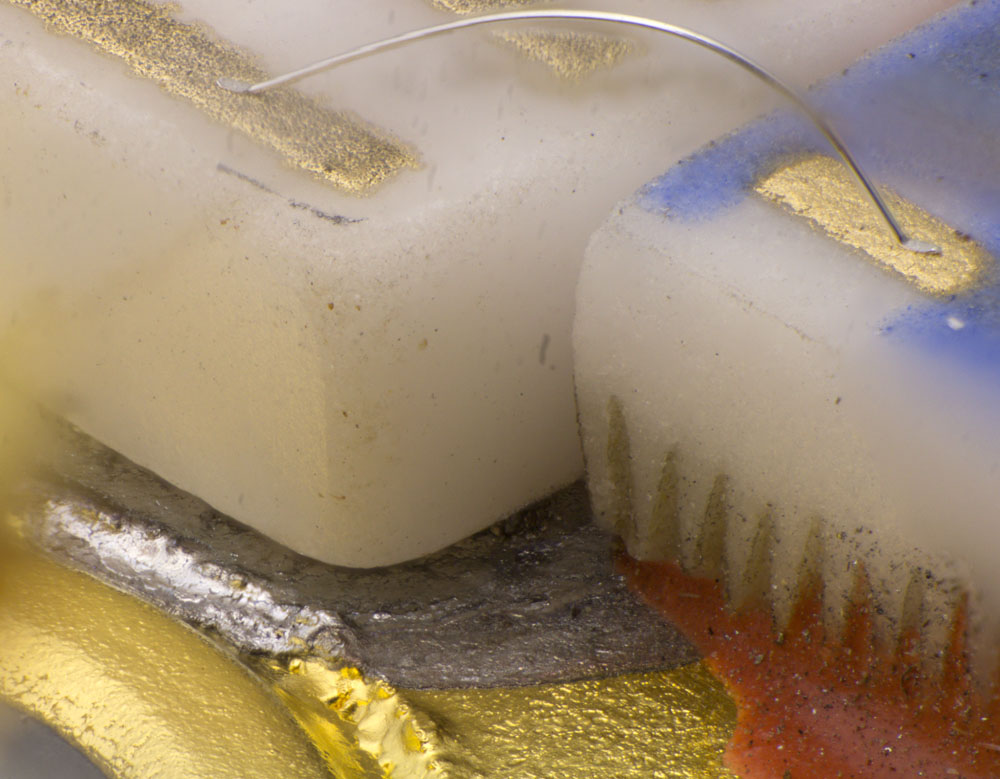


The powerstages were soldered to the package. After that the controlstage was simply glued down. I assume they wanted to protect the controlstage from the heat of the soldering process.
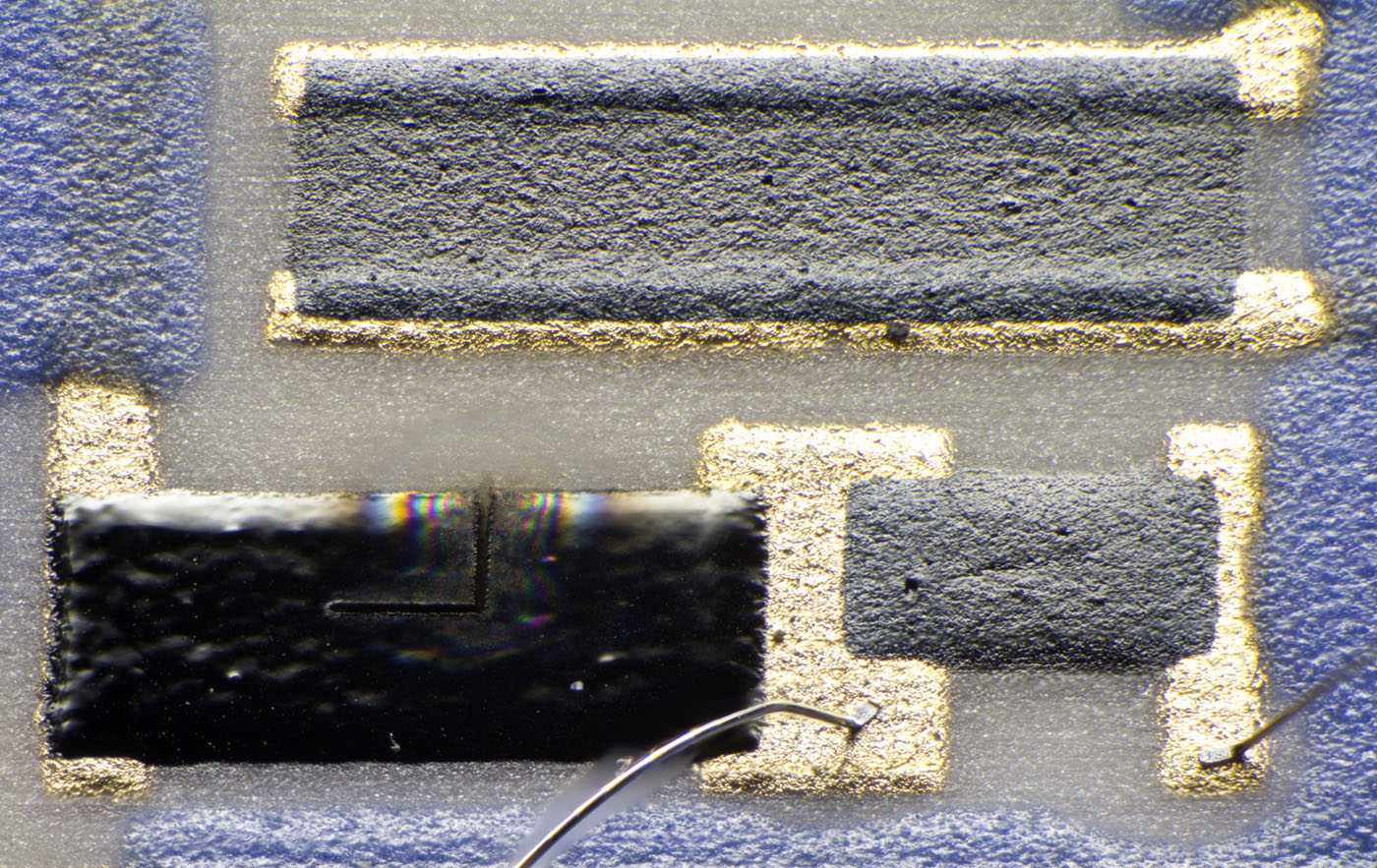


It seems there are three different resistor types, a shiny one, a thin rough one and a thick rough one.
Of course they did laser tuning.
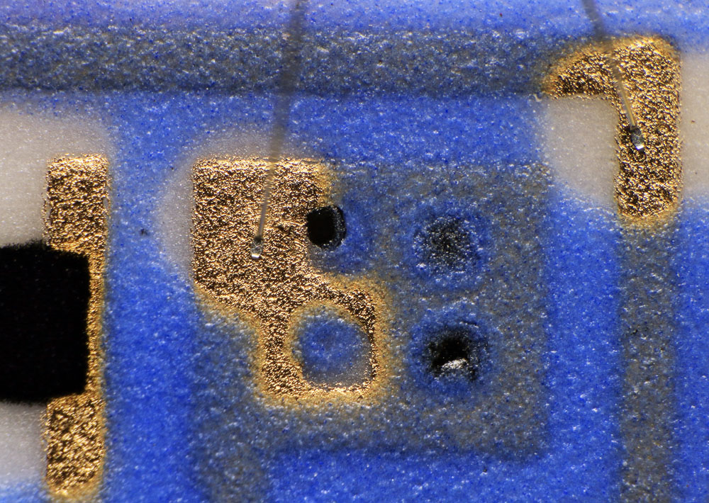


And there are points to identify the aligment of the masks.
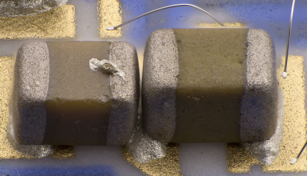


Now that doesn´t look quite robust...  ???


Apex also had problems with the bonding process...
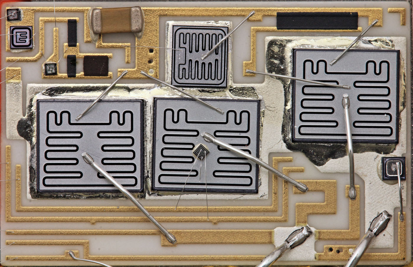


Huuuuuge!  8)
The shunt for overcurrent protection is simply one of the traces leading from a transistor to the output.
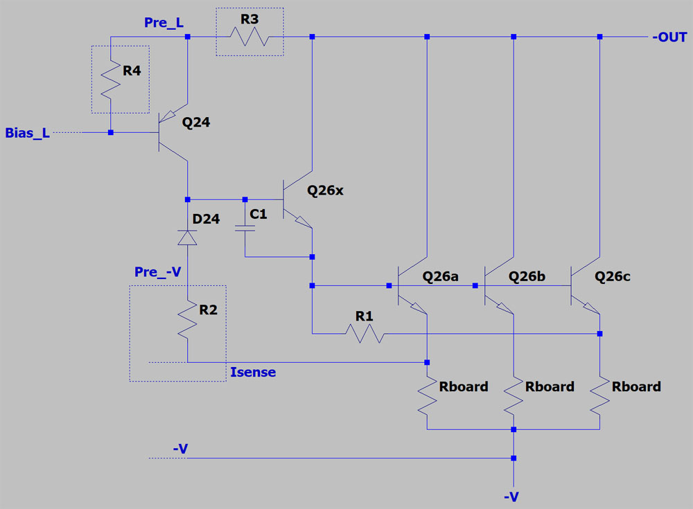


It´s a Sziklai-Darlington-powerstage.
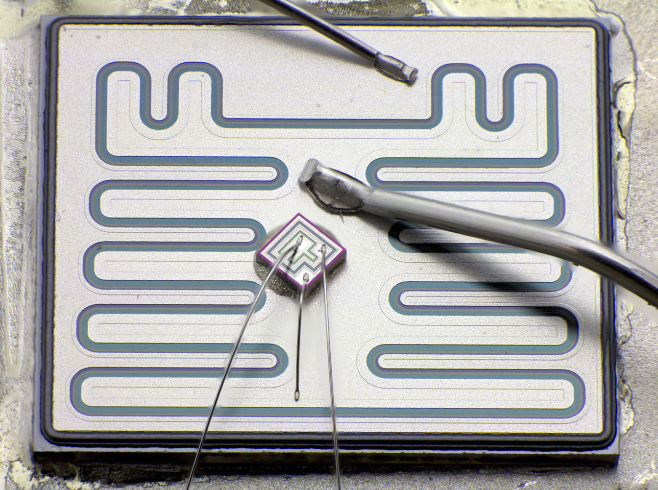


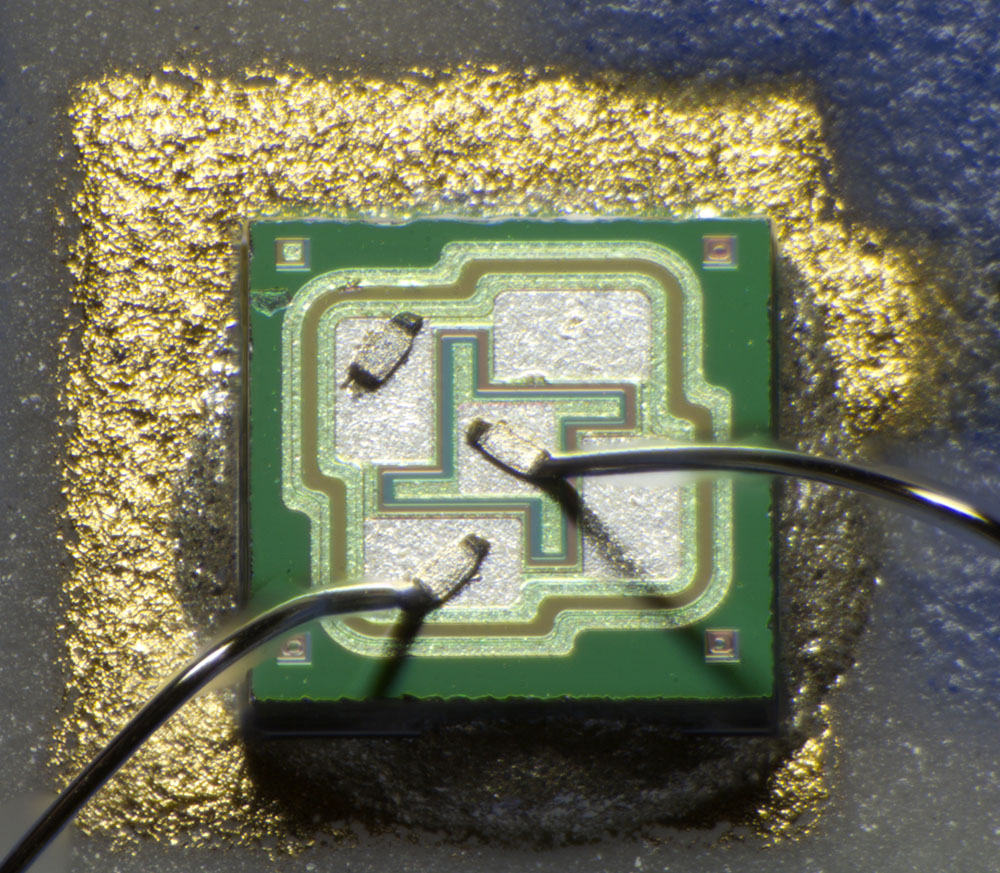
That´s a really good temperature measurement! Datasheet states a response time of 10ms.
You can´t kill the transistors with second breakdown. Second breakdown only is a danger at durations longer than 10ms and there the temperature protection is fast enough.  :box:


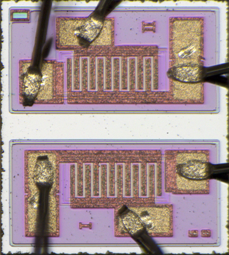
Input stage is of course a Dual-J-FET for most similar characteristics and a similar temperature.


It´s too late for a longer translation. Please use your favourite translator and take a look at a lot more pictures on my website:

https://www.richis-lab.de/Opamp17.htm

Of course you can ask me whatever you want here in english.

 :popcorn:
« Last Edit: October 25, 2020, 10:49:26 pm by Noopy »
 
The following users thanked this post: lowimpedance, TiN, RoGeorge

Offline RoGeorge

  • Super Contributor
  • ***
  • Posts: 6806
  • Country: ro
Re: Opamps - Die pictures
« Reply #80 on: October 25, 2020, 10:27:34 pm »
APEX?!  Like the game?  :D

Offline NoopyTopic starter

  • Super Contributor
  • ***
  • Posts: 1903
  • Country: de
    • Richis-Lab
Re: Opamps - Die pictures
« Reply #81 on: October 25, 2020, 10:28:58 pm »
I´m getting old. Didn´t know there is a game with the name APEX.  ;D :-+

Offline T3sl4co1l

  • Super Contributor
  • ***
  • Posts: 22436
  • Country: us
  • Expert, Analog Electronics, PCB Layout, EMC
    • Seven Transistor Labs
Re: Opamps - Die pictures
« Reply #82 on: October 26, 2020, 01:11:51 am »
They had the name before the game existed.  8)

Handle that thing carefully, those are BeO substrates!  Fantastic heat conduction, worth every cent too... ;D

Tim
Seven Transistor Labs, LLC
Electronic design, from concept to prototype.
Bringing a project to life?  Send me a message!
 

Offline NoopyTopic starter

  • Super Contributor
  • ***
  • Posts: 1903
  • Country: de
    • Richis-Lab
Re: Opamps - Die pictures
« Reply #83 on: October 26, 2020, 04:16:49 am »
Thanks for the hint. It´s not the first BeO-part I have opened. I take care not to cut the ceramic that should be good enough.  :-/O

Offline NoopyTopic starter

  • Super Contributor
  • ***
  • Posts: 1903
  • Country: de
    • Richis-Lab
Re: Opamps - Die pictures
« Reply #84 on: November 02, 2020, 10:14:54 pm »


Let´s look into the famous LM709.


That are very small resistor strings! I have never seen such small resistors (with respect to the transistors).


The pnp-transistor Q9 shows the normal structure of a pnp-transistor manufactured with a npn-process.
But the pnp-transistor Q13 is different! There is a brown emitter area surrounded by the blue, n+ doping. You can´t see a collector. It seems like Q13 uses the substrate as collector. That´s possible because the collector had to be connected to the negative supply. The buried n+ layer was certainly removed. The n+ base contact frame gives you a quite low resistance leading to the active base area.
It would have been possible to use the isolation diffusion as collector but then the base area would have been too long for a good transistor.


https://www.richis-lab.de/Opamp20.htm

 :-/O
 
The following users thanked this post: RoGeorge

Offline David Hess

  • Super Contributor
  • ***
  • Posts: 17214
  • Country: us
  • DavidH
Re: Opamps - Die pictures
« Reply #85 on: November 03, 2020, 01:31:55 am »
But the pnp-transistor Q13 is different! There is a brown emitter area surrounded by the blue, n+ doping. You can´t see a collector. It seems like Q13 uses the substrate as collector. That´s possible because the collector had to be connected to the negative supply. The buried n+ layer was certainly removed. The n+ base contact frame gives you a quite low resistance leading to the active base area.

That sounds suspiciously like a charge storage PNP.  Widlar himself describes it on page 3 of Linear Technology application note 16:

https://www.analog.com/media/en/technical-documentation/application-notes/an16f.pdf
 
The following users thanked this post: Noopy

Offline NoopyTopic starter

  • Super Contributor
  • ***
  • Posts: 1903
  • Country: de
    • Richis-Lab
Re: Opamps - Die pictures
« Reply #86 on: November 03, 2020, 03:54:39 am »
But the pnp-transistor Q13 is different! There is a brown emitter area surrounded by the blue, n+ doping. You can´t see a collector. It seems like Q13 uses the substrate as collector. That´s possible because the collector had to be connected to the negative supply. The buried n+ layer was certainly removed. The n+ base contact frame gives you a quite low resistance leading to the active base area.

That sounds suspiciously like a charge storage PNP.  Widlar himself describes it on page 3 of Linear Technology application note 16:

https://www.analog.com/media/en/technical-documentation/application-notes/an16f.pdf

Thanks for the hint, that´s very interesting.  :-+

I hope I got it right:
Usually you try to minimize base-emitter-capacitance to get a fast transistor (fast switch-off).
In the charge storage PNP-transistor you try to get a bigger base-emitter-capacitance with fast charges so you can boost a signal through this area. (I suppose switch off is slower.)
In the LM709 output stage that would speed up the lowside getting low. I assume a slower switch off speed is not extremly important because the highside can pull the output upwards.

Offline NoopyTopic starter

  • Super Contributor
  • ***
  • Posts: 1903
  • Country: de
    • Richis-Lab
Re: Opamps - Die pictures
« Reply #87 on: November 05, 2020, 09:00:22 pm »


Mikroelektronika Botevgrad 1УO709 - 1UO709, another 709-opamp.


Unfortunately the die was damaged a little.
Nevertheless we can clearly see that it is very similar to the LM709.


https://www.richis-lab.de/Opamp21.htm


 :popcorn:

Offline NoopyTopic starter

  • Super Contributor
  • ***
  • Posts: 1903
  • Country: de
    • Richis-Lab
Re: Opamps - Die pictures
« Reply #88 on: November 09, 2020, 03:39:34 pm »
Let´s take a closer look into a OPA627!  8)


The die is quite big (2,9mm x 2,0mm).


The most interesting part is the input stage. There is a matrix of 2x8 transistors forming the two input transistors. Burr-Brown tried to match the metal traces and the silicon traces as good as possible. In the upper left corner there are two green underpasses which are "very" long and wide just to match the underpasses in the lower right corner.

Around the input transistors there are the tuned resistors for input-offset tuning and the current mirror emitter resistors which travel quite a long way to get to the left edge of the die. I assume they wanted to bring some distance between the transistors and the edge of the die and then decided to fill the empty room with the current mirror resistors.

On the right side there are four transistors generating the two cascode transistors of the input stage. The current sink is placed in the center for most equal temperatures.

Above and below the input transistor matrix there are two more input-J-FETs which are connected to two more transistors in the cascode stage.


The circuit is a bit different to the schematic in the datasheet. I dont´really understand what is the purpose of the path Q17/Q18-Q6/Q7...  :-// @magic: any ideas?  ;)


More pictures here:
https://www.richis-lab.de/Opamp22.htm

 :popcorn:
 
The following users thanked this post: laneboysrc, floobydust

Offline David Hess

  • Super Contributor
  • ***
  • Posts: 17214
  • Country: us
  • DavidH
Re: Opamps - Die pictures
« Reply #89 on: November 09, 2020, 04:18:25 pm »
The circuit is a bit different to the schematic in the datasheet. I dont´really understand what is the purpose of the path Q17/Q18-Q6/Q7...  :-// @magic: any ideas?  ;)

Could that be transconductance reduction of the input stage?  It is not in the form that I usually see and it is almost always left off of published schematics.
 

Offline NoopyTopic starter

  • Super Contributor
  • ***
  • Posts: 1903
  • Country: de
    • Richis-Lab
Re: Opamps - Die pictures
« Reply #90 on: November 09, 2020, 06:46:19 pm »
Could that be transconductance reduction of the input stage?  It is not in the form that I usually see and it is almost always left off of published schematics.

That's possible.  :-+ ...an interesting way of transconductance reduction. Probably a very clever way for the OPA627.  :-//

Offline magic

  • Super Contributor
  • ***
  • Posts: 7246
  • Country: pl
Re: Opamps - Die pictures
« Reply #91 on: November 09, 2020, 08:46:21 pm »
If the schematic is to be believed, these are P channel JFETs like in TL071 so you have drawn them upside down. The sources should be "up", the drains should be "down".

Then it looks like Q17,Q18 are simply source followers and Q6,Q7 diodes shift the voltage one Vbe up and drive bases of Q2~Q5. Input stage current is about 8x the current through Q6,Q7 and Q17,Q18, which is set by that current source at the positive rail.

Q8 and Q1 plus something between them (let me guess: a string of diodes or resistor) bootstrap the drains of all those JFETs.

BTW, zeptobars has a higher resolution image.
https://zeptobars.com/en/read/BB-TI-OPA627-opamp-genuine-fake
« Last Edit: November 09, 2020, 08:50:41 pm by magic »
 

Offline NoopyTopic starter

  • Super Contributor
  • ***
  • Posts: 1903
  • Country: de
    • Richis-Lab
Re: Opamps - Die pictures
« Reply #92 on: November 10, 2020, 04:25:48 am »
Thanks!  :) You are right, the JFETs were rotated. And the numbers were also confusing. I changed that:


Is it correct to call J1-J8/Q2-Q3 a cascode?

I didn´t check the parts between Q8 and Q1 but that should be some kind ob voltage drop.  :-+

That´s an interesting input stage! But why did they double the inputs? Why J17/J18 and Q6/Q7?


I know zeptobars had already pictures but I had to take a look into this one because the owner wanted to know whether it´s genuine.  :-/O

Offline magic

  • Super Contributor
  • ***
  • Posts: 7246
  • Country: pl
Re: Opamps - Die pictures
« Reply #93 on: November 10, 2020, 10:16:52 am »
Not sure. Q6 seems to have ⅛ emitter area of Q2+Q3 and J17 is ⅛ of J1~J8 and the resistors are probably in 8:1 ratio too. These two current paths operate almost identically. The only difference I see so far is that Q6 and J17 current is affected only by Early effect in the current source, but Q2+Q3 and J1~J8 current is affected also by Early effect in Q2+Q3.

Is this difference between J17 and J1~J8 operating current significant? Maybe for THD, or maybe not. Maybe this configuration only plays some role in preventing phase reversal. Maybe they didn't want to do a thermally balanced layout for Q6. Maybe it avoids needing to laser trim R7. Maybe simulation would show something.

BTW, if we connect Q6 emitter to Q2+Q3, we get a configuration analogous to inverted LM101A.
« Last Edit: November 10, 2020, 10:21:57 am by magic »
 
The following users thanked this post: Noopy

Offline NoopyTopic starter

  • Super Contributor
  • ***
  • Posts: 1903
  • Country: de
    • Richis-Lab
Re: Opamps - Die pictures
« Reply #94 on: November 10, 2020, 12:08:45 pm »
Thanks for your interpretation!
A mysterious input stage...  :-/O

Offline David Hess

  • Super Contributor
  • ***
  • Posts: 17214
  • Country: us
  • DavidH
Re: Opamps - Die pictures
« Reply #95 on: November 10, 2020, 04:37:47 pm »
Is it correct to call J1-J8/Q2-Q3 a cascode?

Yes, I was looking at it completely wrong.  Q2 through Q7 are the cascode transistors for J1 through J8 and J9 through J16.

Quote
That´s an interesting input stage! But why did they double the inputs? Why J17/J18 and Q6/Q7?

J17 and J18 control the base voltage of the cascodes so that they follow the input JFETs making Vds is constant.  The base connection between Q6 and Q8 receives a constant current from the positive supply which creates a constant voltage across R7 and R8.  Q6 and Q7 are connected as diodes so that their Vbe compensates the Vbe of the cascode transistors.

A cascode configuration is common with super-beta input stages because the Vce breakdown voltage is very low, only like 3 to 5 volts.  Sometimes it is used to increase the differential input voltage range by preventing breakdown of base-emitter junction of the input transistors.  I do not know why it would be used with JFETs unless modulation with changing drain voltage was a significant error term, which it could be.  Or maybe these JFETs have a limited maximum Vds?
 
The following users thanked this post: PartialDischarge, Noopy

Offline NoopyTopic starter

  • Super Contributor
  • ***
  • Posts: 1903
  • Country: de
    • Richis-Lab
Re: Opamps - Die pictures
« Reply #96 on: November 10, 2020, 05:20:55 pm »
That´s an interesting input stage! But why did they double the inputs? Why J17/J18 and Q6/Q7?

J17 and J18 control the base voltage of the cascodes so that they follow the input JFETs making Vds is constant.  The base connection between Q6 and Q8 receives a constant current from the positive supply which creates a constant voltage across R7 and R8.  Q6 and Q7 are connected as diodes so that their Vbe compensates the Vbe of the cascode transistors.

A cascode configuration is common with super-beta input stages because the Vce breakdown voltage is very low, only like 3 to 5 volts.  Sometimes it is used to increase the differential input voltage range by preventing breakdown of base-emitter junction of the input transistors.  I do not know why it would be used with JFETs unless modulation with changing drain voltage was a significant error term, which it could be.  Or maybe these JFETs have a limited maximum Vds?

That is convincing, thanks!  :-+

Offline David Hess

  • Super Contributor
  • ***
  • Posts: 17214
  • Country: us
  • DavidH
Re: Opamps - Die pictures
« Reply #97 on: November 10, 2020, 05:33:32 pm »
I wonder what advantages this topology would have in a discrete design, with JFET (or bipolar) followers driving common-base bipolars to make a differential input stage.  Noise will be higher.

Incidentally, some people object to calling it a cascode and consider it a cascade (?) when it is the emitter or source of the input transistor driving the emitter or source of a cascode transistor and the transconductance is controlled by the emitter and source resistances plus any added resistance as in this case.

If you squint a little, then it is a differential pair made up of complementary transistors and in this case, completely different types of transistors.  I have run across this complementary differential pair before in high frequency and high frequency high voltage circuits.
« Last Edit: November 10, 2020, 05:35:23 pm by David Hess »
 

Offline Kleinstein

  • Super Contributor
  • ***
  • Posts: 14859
  • Country: de
Re: Opamps - Die pictures
« Reply #98 on: November 10, 2020, 06:02:08 pm »
Keeping the DS voltage of the input JFETs about constant also helps getting a constant and reduced input capacitance. With conventional JFET OPs the bootstrapping may extend to not just the drain voltage, but also to the isolation from the substrate.  AFAIK the OPA627 is a kind of SOI device and does not use the conventional junction isolation, so it would not need this extra step.

One weakness of JFET amplifier is a voltage dependent input capacitance that can create THD.
 

Offline magic

  • Super Contributor
  • ***
  • Posts: 7246
  • Country: pl
Re: Opamps - Die pictures
« Reply #99 on: November 10, 2020, 06:15:55 pm »
Indeed, high source impedance and variable input capacitance form a variable RC lowpass which (slightly) attenuates positive and negative half-cycles by different amount and distorts the waveform.

OPA6x7 are clearly advertised as dielectric-isolated ICs and have long been known as good performers in this regard. More recently, TI claims that OPA140/OPA1641 offer similar performance. Perhaps they came up with some cheaper SOI process.

Bipolar opamps have similar problems with high source impedance. Their BC capacitance isn't constant and neither are base currents.


Share me

Digg  Facebook  SlashDot  Delicious  Technorati  Twitter  Google  Yahoo
Smf