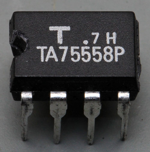
Toshiba TA75558 dual-opamp
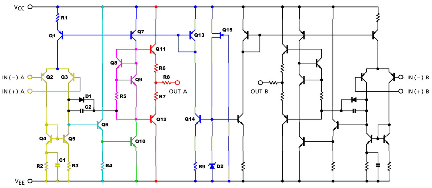
The circuit is quite common.
There is a small mistake. Around the bias circuit for the output stage there are two connection dots missing (one the right side, on the left side the mistake is corrected).
I´m not perfectly sure about D1. What exactly is the purpose of this diode? A DC-path to the output? In theory without external circuitry the output level is undefined.

(@magic?

)
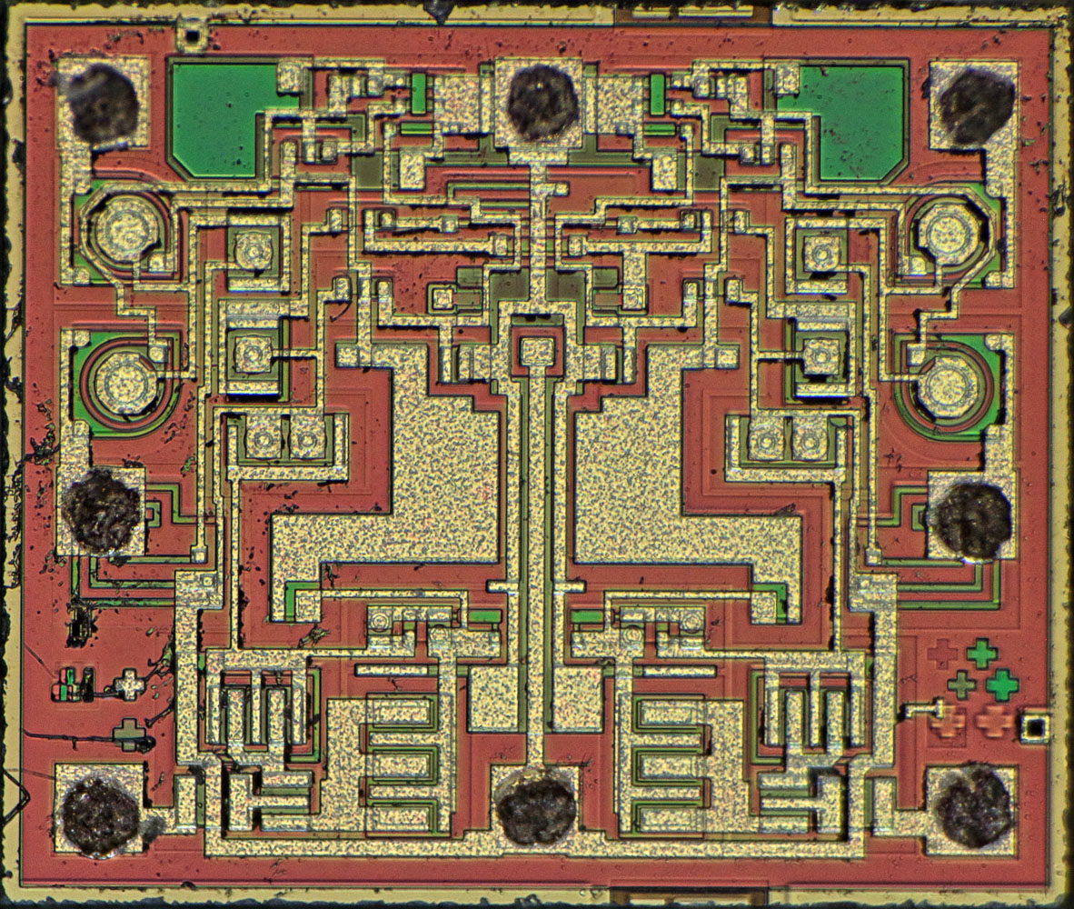
The die is 1,4mm x 1,2mm and quite symmetrical.
#
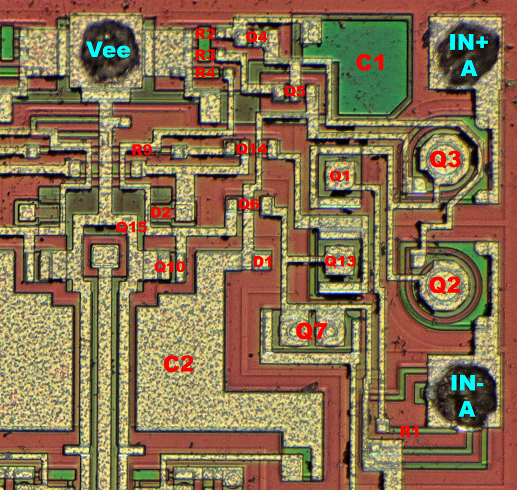
Identifying the parts is no bigger problem.
In the input stage there are round pnp-transistors.
They used pinch resistors to save silicon area. It´s interesting they didn´t use a pinch resistor for R1 therefore it got very long.
C1 refers to the negative supply and because of that just needed a green area against the substrate. In contrast C2 uses the green layer and the metal layer.
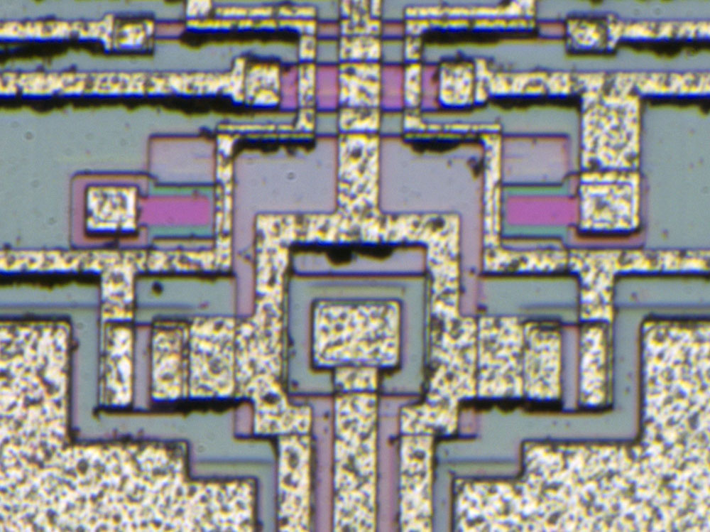
D2 is integrated on both sides of the die but got connected only on the right side.
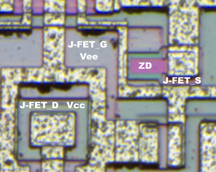
Q15 and D2 are not really easy to spot.
The J-FET Q15 seems to consist of an area that is connected to Vcc and the bias circuit in the upper right corner. On top of this area there is a layer connected to Vee. The lower layer is probably n-doped and the upper layer is p-doped so you get the J-FET you need.
There is a reddish stripe going into the Vee-area. That´s probably the highly n-doped emitter material which gives you a zener to Vee.
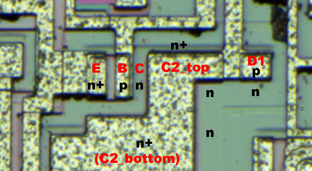
Q10, D1 and C2 are also interesting parts.
Q10 collector potential is the same as the potential of the lower C2 electrode. Because of that Q10 has no own collector contact but is integrated in the surrounding n-doped area of C2. Since the lower electrode of C2 is highly n-doped and there is a buried highly n-doped layer under all the parts there is a low impedance connection between Q10 collector and the lower potential of C2.
D1 is connected in parallel to C2. Because of that D1 is constructed by integrating a small p-doped area in the n-doped area around C2 and connecting it to the upper metal electrode of C2. You can see the outlines of the contact and the p-doped area in the metal layer.
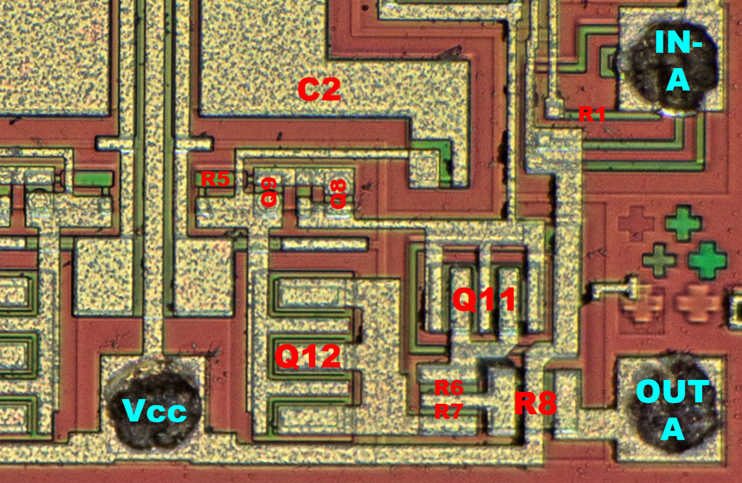
The output stage contains two big transistors with one dual emitter resistor and the output resistor leading to the output bondpad.
The output stage bias circuit is integrated in a small area that acts as a collector for both transistors.
Some more pictures:
https://www.richis-lab.de/Opamp28.htm 