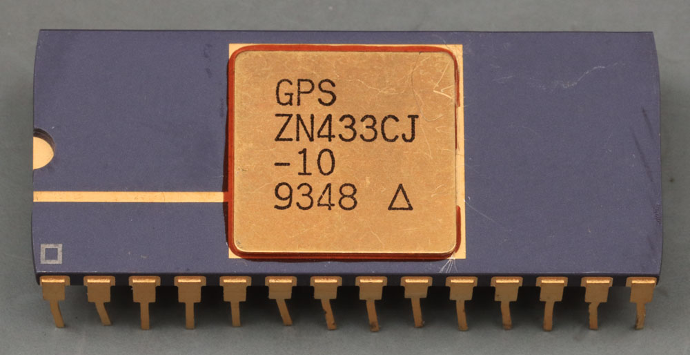
The ZN433 is a so-called tracking ADC. It was developed by Ferranti. It is said to be the first fully integrated 10-bit tracking ADC. GPS stands for GEC Plessey Semiconductors. GPS took over Ferranti in 1987.
The index CJ marks the bin with the smallest operating temperature range (0°C-70°C). The best bin guarantees its specifications in a temperature range between -55°C and 125°C. The number 10 indicates that this is the variant with a resolution of 10 bits. Variants with resolutions of 9Bit and 8Bit were also available. The structure is always the same, but the accuracy is correspondingly poorer.
The ZN433 requires a +/-5V supply and consumes 50mA. The datasheet specifies a maximum non-linearity of +/-0,5LSB. The temperature coefficient of the amplification factor is typically 10ppm/°C. The offset drift is specified in the datasheet as 7ppm/°C FSR.
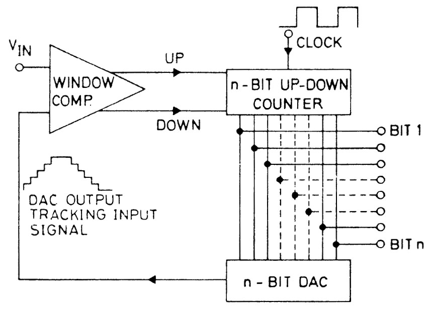
In the "Technical Handbook Standard ICs" from 1984, Ferranti shows how a tracking ADC does the conversion. A comparator compares the input signal with the value of a DAC. Depending on whether the input signal is larger or smaller, the value in a counter is reduced or increased. The value of the counter serves as the input signal for the DAC and simultaneously represents the digital output signal.
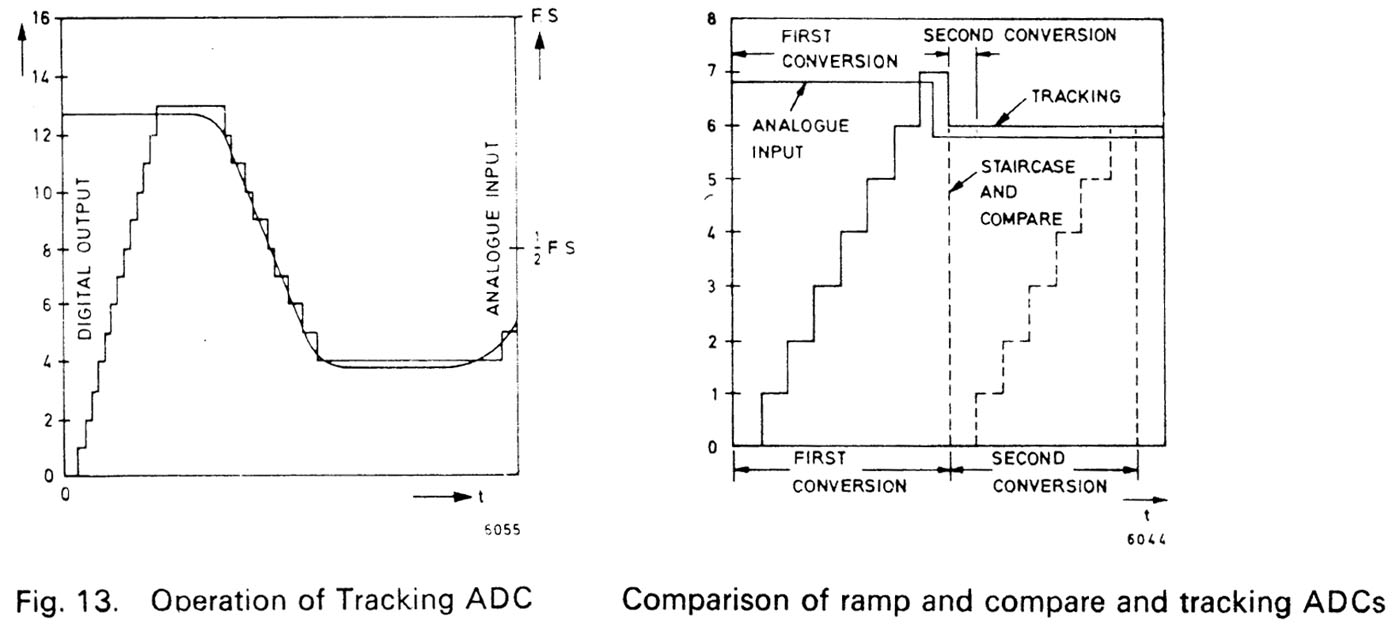
In the image on the left, Ferranti shows how the digital output signal of the tracking ADC follows the input signal. Initially, it takes a relatively long time for the output signal to correspond to the input signal. With the subsequent drop in the input voltage, the ADC can follow quickly and continuously supplies a digital value with only a small error component.
The picture on the right shows the difference to a simple ramp ADC. During the first digital conversion, both ADCs behave in the same way. The ramp ADC requires a similar time for the second digital conversion, while the tracking ADC outputs the new value after just one clock pulse. The specifications of the ZN432 give a feeling for the time advantage. The ZN432 is very similar to the ZN433, but uses the SAR principle. It needs 20µs to output the next value, whereas the ZN433 delivers the next value after just 1µs.
The great advantage of a tracking ADC is that it outputs a valid digital value at all times and is quite fast. A disadvantage is that the error of the digital value fluctuates greatly if the input signal changes faster than the comparison signal can change. In addition, the LSB changes continuously even with a constant input signal. In this respect, the illustration on the left is obviously not quite correct.
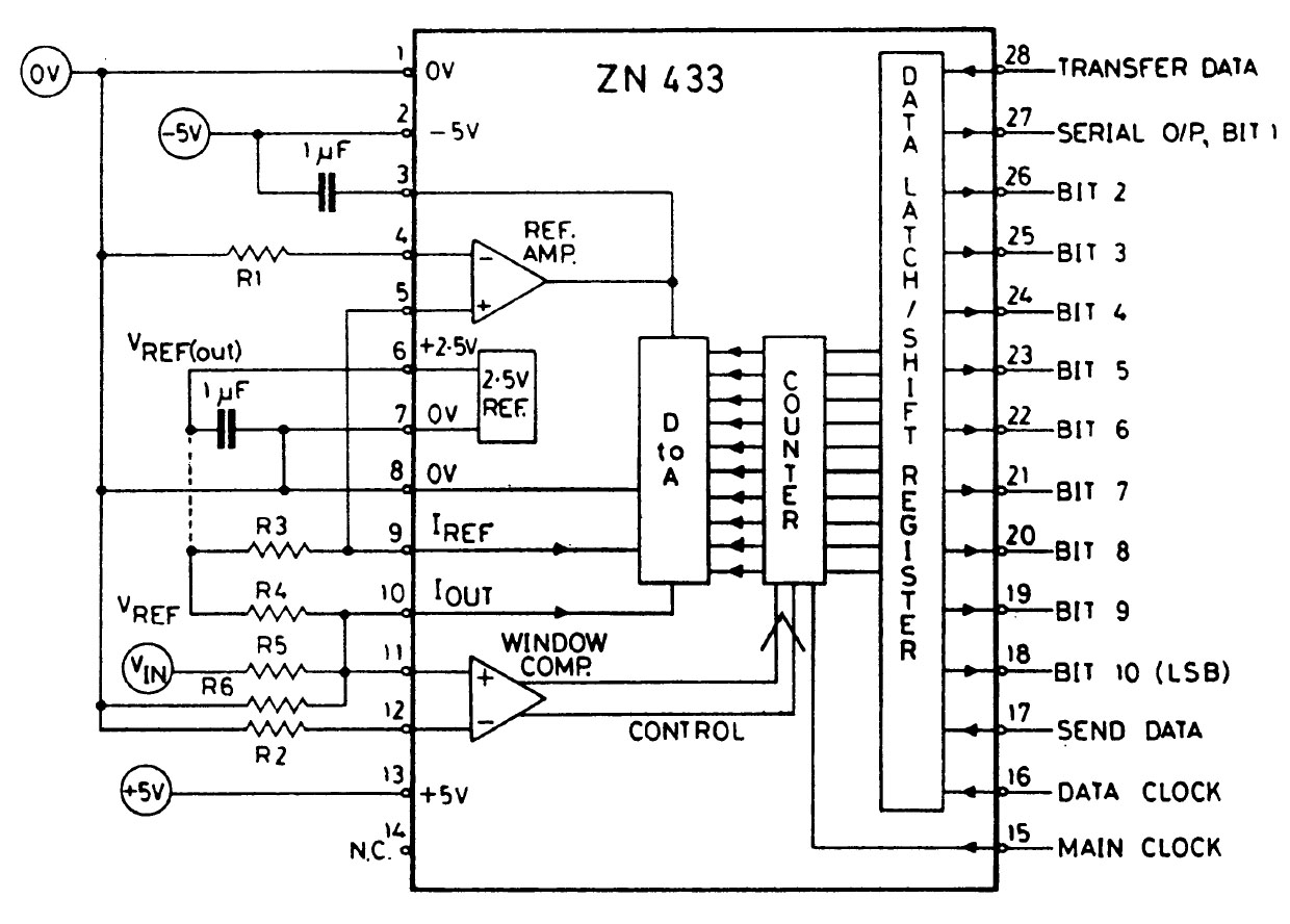
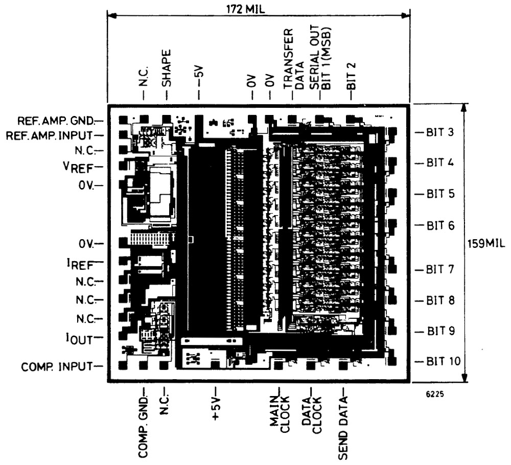
The ZN433 datasheet contains a block diagram. Apart from the resistors that define the input voltage range, the module contains all the necessary components. The input voltage range can be set unipolar up to +5V or bipolar up to +/-10V. The buffer memory in the ZN433 enables the digital value to be read out in parallel or serially.
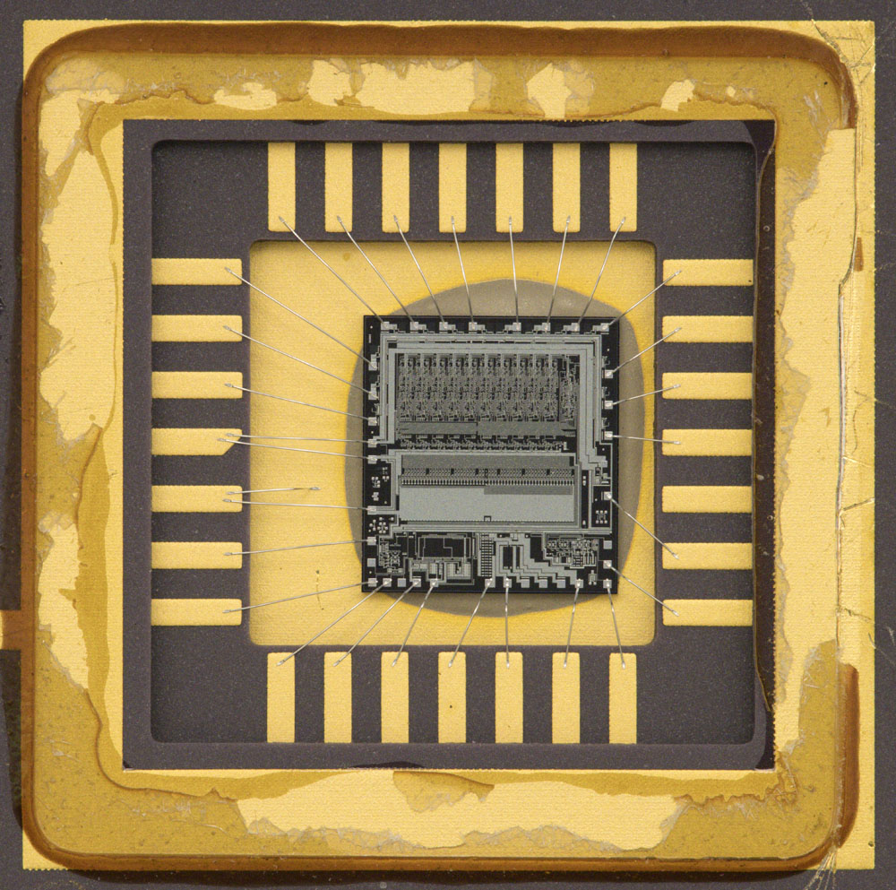
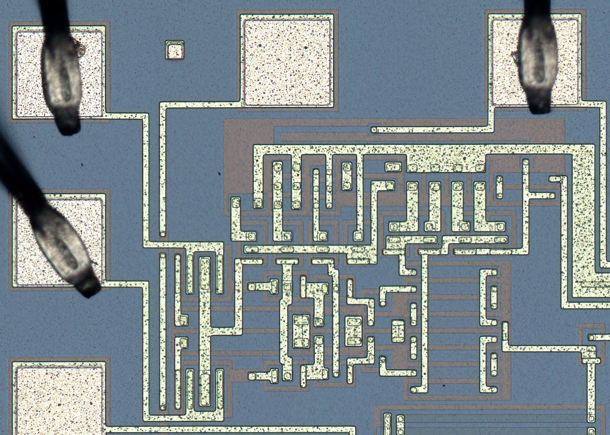
The -5V potential is connected to the bottom of the package and through this to the substrate. The reference potential is routed to the ADC with two bondwires.
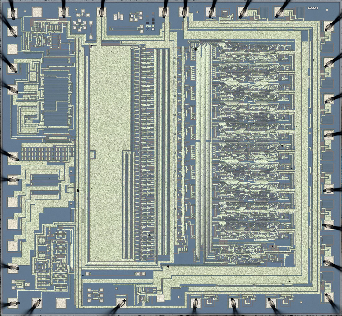
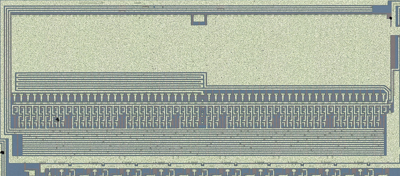
The dimensions of the ZN433 are 4,43mm x 4,10mm. The die contains some unused bondpads. This image is also available in higher resolution:
https://www.richis-lab.de/images/ADC/07x07XL.jpg (26MB)
The datasheet contains an illustration of the metal layer. The dimensions and structures match the die in this ZN433. The function of the unused bondpads is not described.
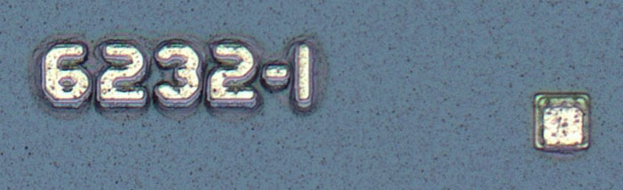
6232-1 could be the internal designation of the design.
Various test structures are integrated at the top edge and in the bottom left-hand corner. There are also illustrations of some masks in the upper area.
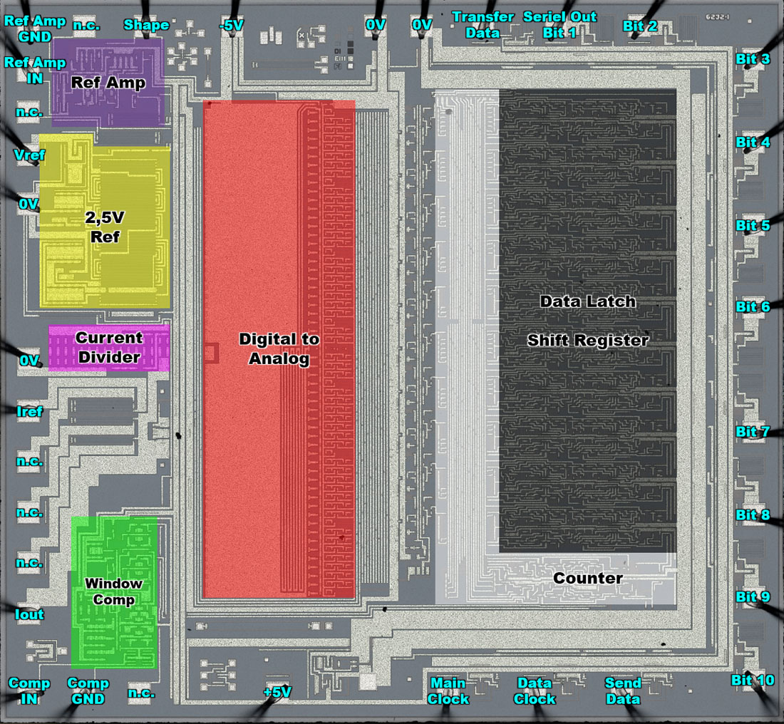
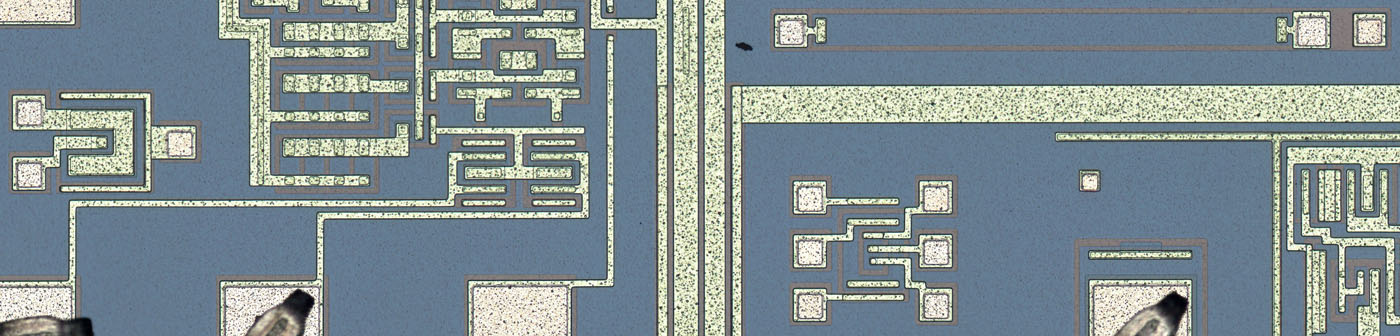
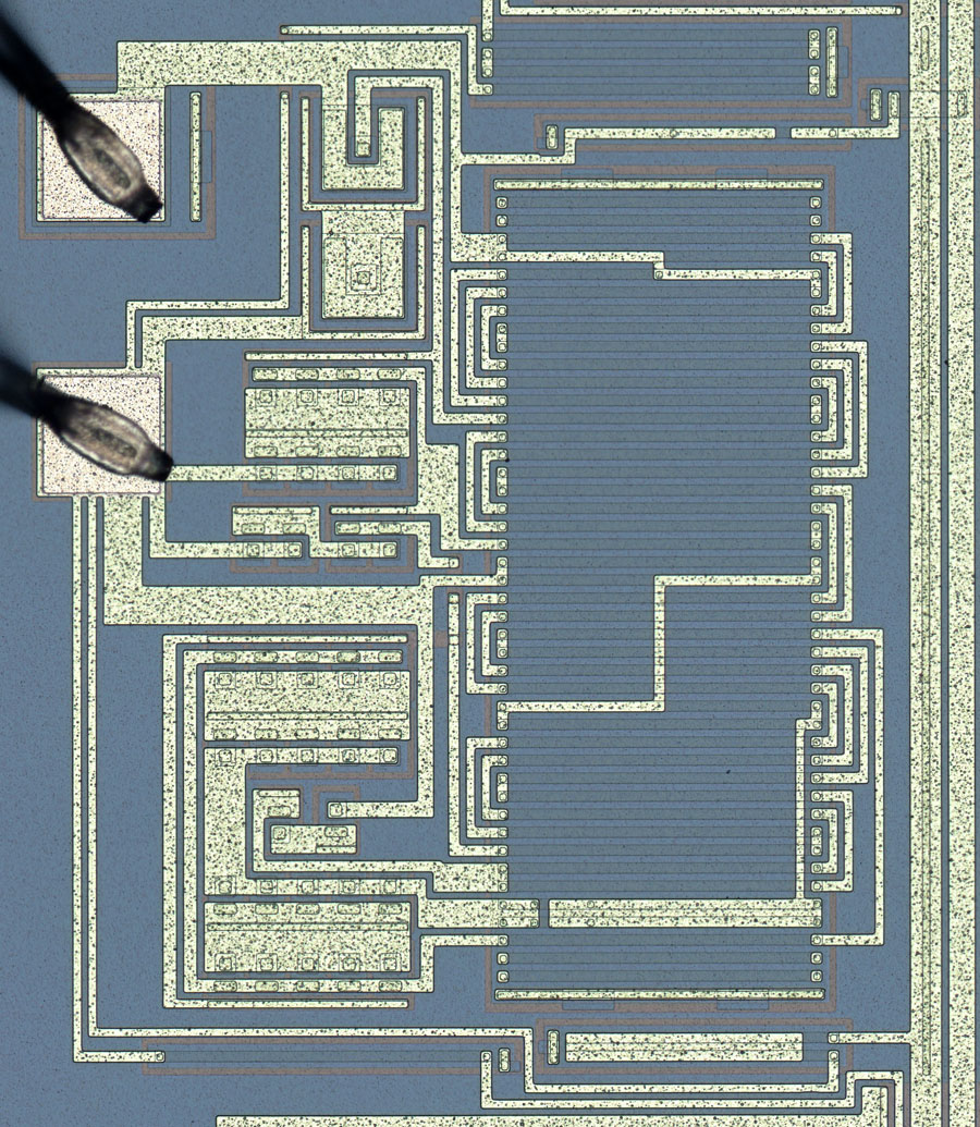
The digital part of the ADC is located on the right-hand side of the die. The buffer memory (black), which also serves as a shift register for the serial data output, can be clearly recognized by its repeating structures. The counter (white) is located in the bottom right-hand corner and controls both the DAC and the buffer memory. The comparator (green) controls the counter with two signals.
The DAC (red) occupies a relatively large area in the middle. In order to be able to display the very different current values, there is a current divider (pink) at the output. Based on the reference voltage source (yellow), an operational amplifier (purple) sets the reference current with which the DAC operates.
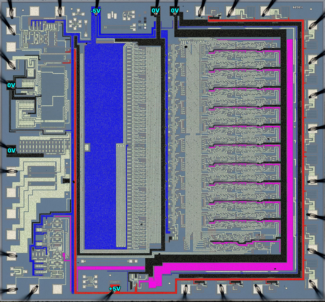
Considerable effort has been made to transfer the supply potentials to the respective circuit parts with as little interference as possible. The +5V potential (red) supplies the digital inputs and outputs, the reference voltage source and the opamp that regulates the currents in the DAC. A further supply is also generated from the +5V potential (pink). This potential is used by the digital part and the comparator. This is probably intended to attenuate feedback from the digital part to the analog circuit parts.
The reference potential (black) is routed four times to the die. One bondpad operates the digital section. Two separate lines ensure that the states of the digital interfaces do not influence the counter and the buffer memory. Another bondpad is connected to the DAC, the opamp and the comparator. The reference voltage source has its own reference potential, as does the current divider, which constantly processes fluctuating currents.
The -5V potential (blue) is largely distributed in a star shape from one bondpad. One line covers the digital part and contacts the substrate over a large area. Another line is used to control the DAC. There is a metal surface above the large resistors of the DAC, which is connected to the -5V potential. The left ends of the resistors are connected to this metal surface. The opamp of the DAC and the comparator have their own -5V line, which also contacts the substrate several times on its way.
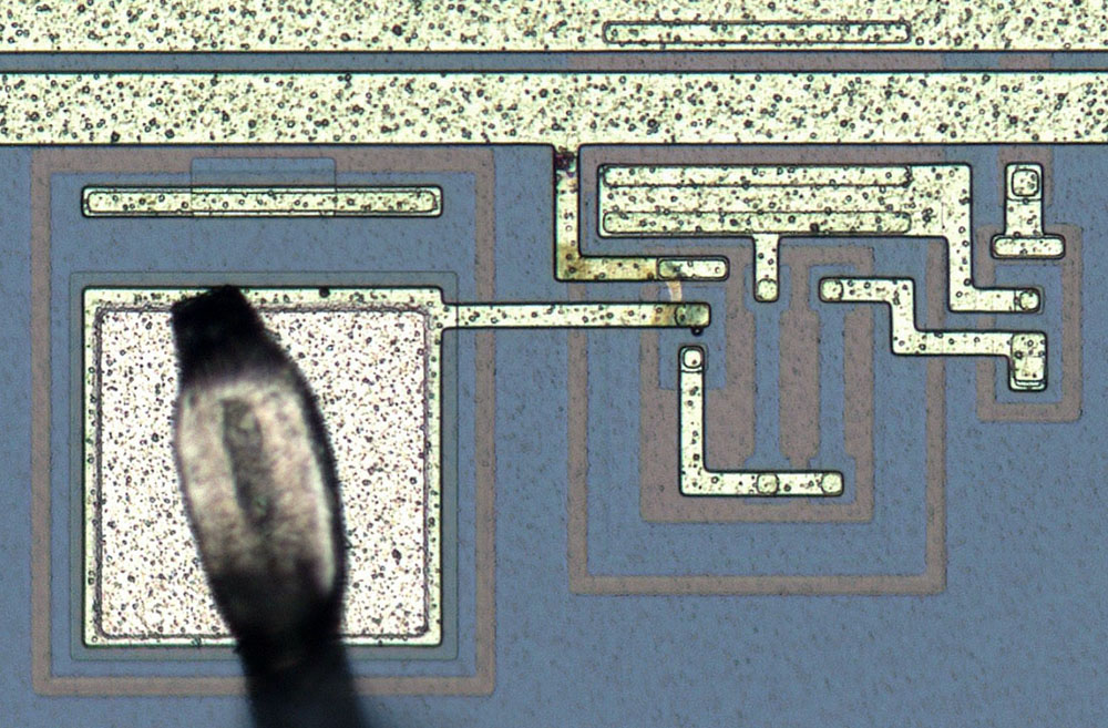
The additional supply potential is generated by a very simple voltage regulator from the +5V potential. A contact pad is located within the additional potential. It is significantly larger than all other testpads, but slightly smaller than the bondpads. This pad is not marked in the overview in the datasheet. It is probably only used for test purposes, perhaps for more regular tests where a larger contact pad was desirable.
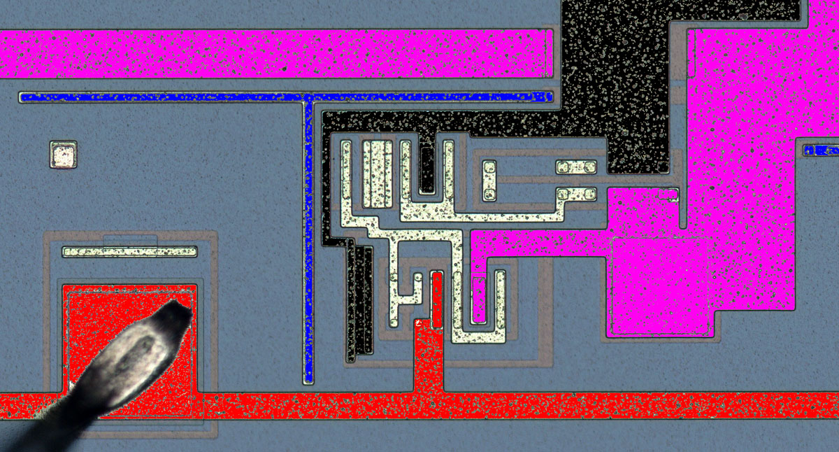
The data clock input can be seen here. The discoloration suggests that the collector-base junction in the input transistor has broken through.
The outputs consist of a pull-up resistor and a large transistor. The transistor has an unusual design. It appears to be a PNP transistor.
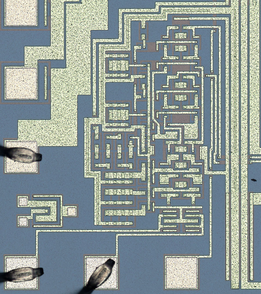
The reference voltage source is based on a bandgap reference. It is particularly interesting that all transistors consist of two transistors connected in series. The lower transistor is always connected as a diode.
The integrated resistors are extensively divided and interleaved so that they behave as equally as possible and temperature gradients do not have too great an influence.
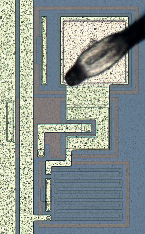
There is an unused bondpad in the area of the opamp that regulates the current sinks in the DAC. This bondpad can be used to contact a resistor that leads to the reference potential. Apparently, the option of connecting this resistor to the opamp with a bond variant has been reserved here, thus eliminating the need for an external resistor.
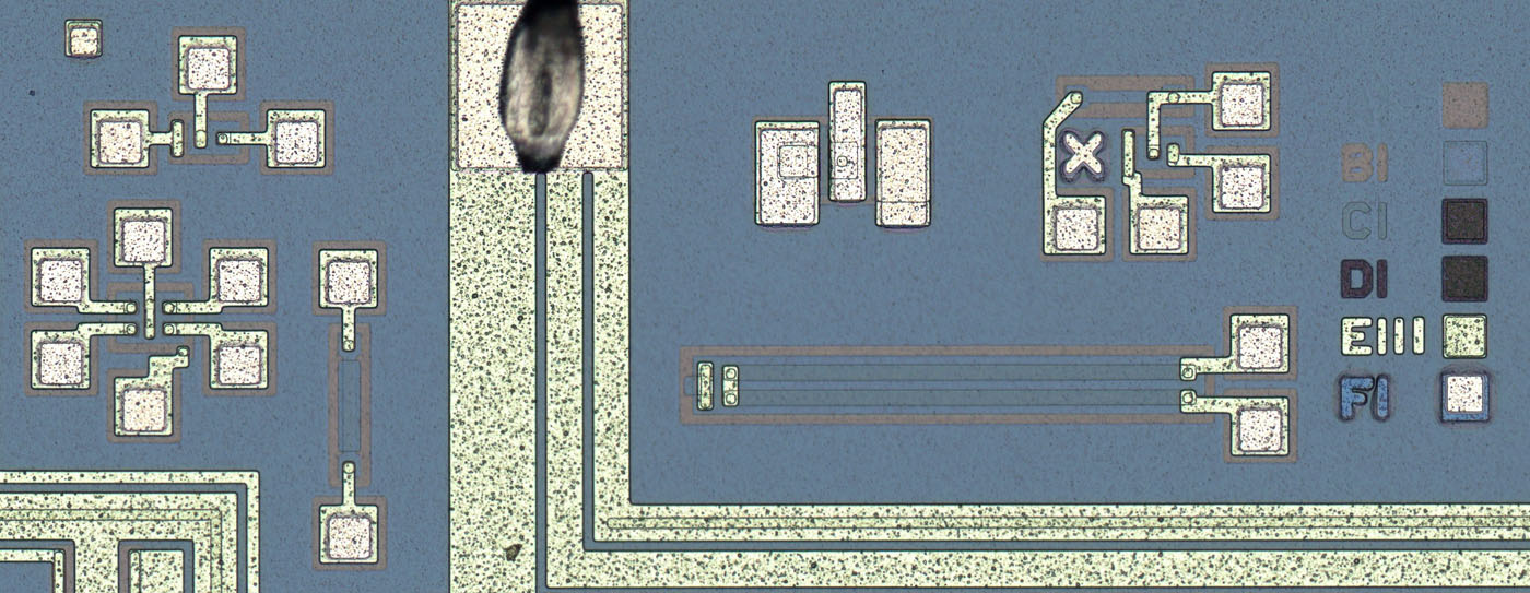
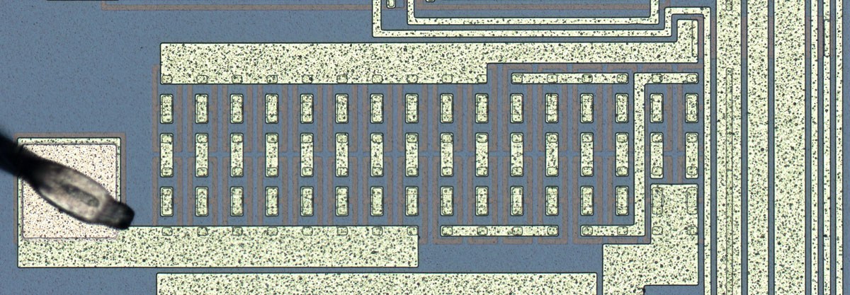
The DAC consists of a whole series of large resistors, which are covered by a large metal surface. The contacts to the resistor strips can be seen on the upper edge of the surface. Below the metal surface are the transistors which, in combination with the resistors, represent the current sinks and switch the currents through.
The large loops that describe the metal layer in the left-hand area are interesting. This is the potential that controls the current sinks. It is generated at the right edge and from there led to the left. Presumably the loops compensate for something.
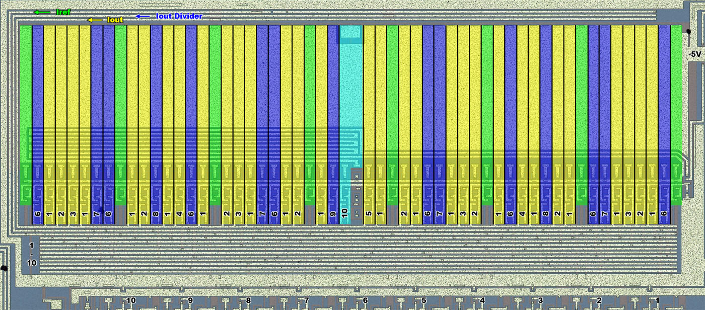
The ten control lines are fed in from below. Ten horizontal lines distribute the potentials along the current sinks. The reference current sink consists of 8 current sinks, which are distributed across the DAC (green). Some current sinks contribute directly to the output current (yellow). The other current sinks are divided via the current divider (blue/cyan).
Bit 1 activates 16 current sinks. Bit 2 activates only 8 current sinks. The ratio of the first five current sinks is 16:8:4:2:1. For the current sinks that run via the current divider, the ratio is 8:4:2:1:0,5. The current sink of the tenth bit has a slightly different structure. Here, two of the resistor strips are connected in series.
The current divider consists of a large number of small resistors. This design probably reduces the effect of parasitic properties such as the contact resistance of the contacts. Between the DAC and the reference potential there is effectively the resistance of half an element, while between the DAC and the output there is the resistance of 7,5 elements. The last two elements are bridged by the metal layer. This results in a ratio of 1:15. One would expect a ratio of 1:16. The missing part is probably due to the wiring. The 2x4 blocks in the right hand area are connected several times with just one single wire.
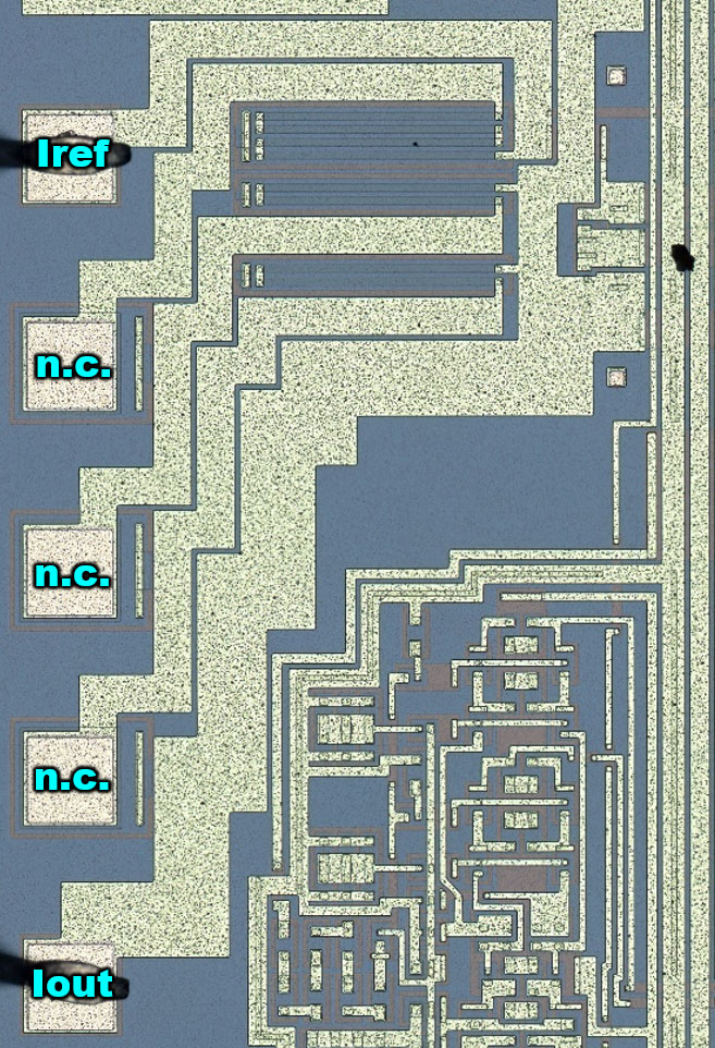
Several resistors are integrated between the Iref and Iout bondpads and connected to three unused bondpads. Obviously, further external resistors could be saved here.
There are four diodes in the upper right area. They limit the voltages of the Iref and Iout potentials in relation to the reference potential.
In the comparator, an unused bondpad enables the connection of a further integrated resistor. This means that the ZN433 could be operated entirely without external resistors.
https://www.richis-lab.de/ADC07.htm 


