Author Topic: Need advice for ADC Buffer  (Read 25587 times)

0 Members and 1 Guest are viewing this topic.

Offline CrossphasedTopic starter

  • Regular Contributor
  • *
  • Posts: 129
  • Country: us
Re: Need advice for ADC Buffer
« Reply #50 on: January 14, 2018, 03:00:54 am »
Well,
I fried the chip! Its not responding anymore. No big deal, I have another one on hand exactly for this situation. I didn't even get to see any smoke come out!  I think a great thing would be if defibrillators worked for electronics, to restart their "heartbeat" so to say!

I'll chalk that one up to learning. Sometimes the best learning happens through mistakes.It certainly seems to cement the lesson. I'm going to replace the chip tonight and consult here before anymore testing. What would you guys suggest for a test circuit sans the operational amplifiers? My goal was to get a sanity check that I was reading the ADC correctly.  Here's the setup I was using:


My apologies if this was a silly mistake to make. I guess my confusion comes from page 2 on the datasheet, which says the analog voltage can be from -3.V to Vcc+ .3V. For this particular ADC, is it only supposed to be used in differential mode? I guess I'm still not completely sure.

So according to Table 2 in the datasheet, the max differential voltage you can measure is Vref/2 to -Vref/2.  With -Vref == ground, would that mean the most positive voltage I can measure is +2.4V? So, if I will only be measuring positive voltages, I should set the common mode input voltage to be -2.5V to utilize the full range? I'm sure this is a very basic thing for you guys but I'm still learning here!
Cheers!
 

Offline David Hess

  • Super Contributor
  • ***
  • Posts: 17241
  • Country: us
  • DavidH
Re: Need advice for ADC Buffer
« Reply #51 on: January 14, 2018, 04:53:59 am »
I guess I have misunderstood the range of inputs. I was under the impression with a reference of +5V, I could measure inputs between 0-5V. But what I'm understanding from you is that I can measure inputs of-2.5V to +2.5V. Is that the case?

The differential Vref sets to total range of the differential Vin centered on zero volts so a 5 volt Vref yields a differential Vin range of -2.5 to +2.5 volts.

Quote
My apologies if this was a silly mistake to make. I guess my confusion comes from page 2 on the datasheet, which says the analog voltage can be from -3.V to Vcc+ .3V. For this particular ADC, is it only supposed to be used in differential mode? I guess I'm still not completely sure.

And this is where you can get into trouble.  While the differential Vin range is +/- Vref/2, each input has to stay between Vcc and Ground.  In practice this means either applying a differential signal to Vin or tying Vin- to Vref/2 and using that as a common for a single ended signal within the range of +/- Vref/2.

Quote
So according to Table 2 in the datasheet, the max differential voltage you can measure is Vref/2 to -Vref/2.  With -Vref == ground, would that mean the most positive voltage I can measure is +2.4V?

Actually +2.5 volts if Vref is +5.0 volts.

Quote
So, if I will only be measuring positive voltages, I should set the common mode input voltage to be -2.5V to utilize the full range? I'm sure this is a very basic thing for you guys but I'm still learning here!

I think they make a different ADC if you want to do this but you cannot set the common mode voltage to be below ground with this part.  None of the inputs may go below ground or above Vcc.
 
The following users thanked this post: Inverted18650

Offline CrossphasedTopic starter

  • Regular Contributor
  • *
  • Posts: 129
  • Country: us
Re: Need advice for ADC Buffer
« Reply #52 on: January 14, 2018, 09:19:43 am »
Wow David,

As usual thank you for your wealth of knowledge and experience. Thank you for clarifying that for me. I literally had no idea. I've seen some other writeups of people using the LTC2400, and I very wrongly assumed the 2440 had the same input parameters.

For simplicity I'm going to limit inputs to the 0-2.5V input range. This leads to  an interesting situation regarding input protection. Now to clamp the +Vin voltage to 2.5V, I will need to provide a +2V rail that a diode or jfet can point to right? Given this recent error of mine, I think it would be wise to implement some input protection. As I understand it though, the protection will be placed in front of the op amps rather than in front of the ADC.

Are comparators ever used for input protection? For example if a comparator trips, then the comparator drives a fet that shorts the input?

On a positive note I replaced the ADC this evening. It was a little tricky with the shielding in the way but it was completed succesfully. Also on a positive note- prior to me applying the full Vref to the input, the ADC was performing quite nicely. I was getting very repeatable readings with very little "jumping around" of the reading. It was encouraging and I definitely see the potential in this project.

On a tangent- today I watched the EEV blog teardown of the Siglent SDM3055 5.5 digit multimeter. It also has a 24 bit delta sigma ADC, the AD7190. It seems similar to the one I'm using, but with a programmable gain amplifier. It was interesting because I was under the impression most commercial multimeters use a dual slope method to sample the input.
 
The following users thanked this post: Inverted18650

Offline Kleinstein

  • Super Contributor
  • ***
  • Posts: 14895
  • Country: de
Re: Need advice for ADC Buffer
« Reply #53 on: January 14, 2018, 11:00:19 am »
It is quite normal for 4-5.5 digit meters to use SD converter chips. The more modern DMM chipsets are also likely SD based.
Dual slope converts are limited in linearity by the capacitor, unless special compensation is used. So they were used mainly for lower resolution.

The input range for the LTC2440 is only +-2.5 V, however AFAIK there should be no damage to the chip if both inputs stay inside the supply range even if the ADC goes well above its nominal range - the ADC just goes to saturation. One can use the ADC in a kind of single input way, but to get the best linearity specified one might have to keep a constant common mode voltage.
 

Offline David Hess

  • Super Contributor
  • ***
  • Posts: 17241
  • Country: us
  • DavidH
Re: Need advice for ADC Buffer
« Reply #54 on: January 14, 2018, 05:26:05 pm »
For simplicity I'm going to limit inputs to the 0-2.5V input range. This leads to  an interesting situation regarding input protection. Now to clamp the +Vin voltage to 2.5V, I will need to provide a +2V rail that a diode or jfet can point to right? Given this recent error of mine, I think it would be wise to implement some input protection. As I understand it though, the protection will be placed in front of the op amps rather than in front of the ADC.

Like Kleinstein says, the input only needs to be clamped between ground and Vcc to prevent damage; differential voltages greater than Vref/2 are not a problem.

If the operational amplifier could drive the inputs beyond ground or Vcc, then they might be clamped in some applications.

Also remember that the operational amplifier cannot by itself drive its output all the way to ground.  If you want to reach zero, then either the operational amplifier will require a negative supply or the ADC input will need to be offset above ground by a little bit.

Quote
Are comparators ever used for input protection? For example if a comparator trips, then the comparator drives a fet that shorts the input?

That can work but comparators do not have high impedance inputs.  Diode clamps should be easier.

Quote
On a tangent- today I watched the EEV blog teardown of the Siglent SDM3055 5.5 digit multimeter. It also has a 24 bit delta sigma ADC, the AD7190. It seems similar to the one I'm using, but with a programmable gain amplifier. It was interesting because I was under the impression most commercial multimeters use a dual slope method to sample the input.

I think the difference is that integrated dual-slope converters are limited to about 40,000 counts but are cheaper than similar delta-sigma converters.  Above this, delta-sigma converters are good to at least 400,000 but cost more.  Above this, custom dual-slope converters become economical.
 

Offline Kleinstein

  • Super Contributor
  • ***
  • Posts: 14895
  • Country: de
Re: Need advice for ADC Buffer
« Reply #55 on: January 14, 2018, 06:08:14 pm »
The dual slope converters can be rather cheap, like the ICL7106 or 7135 for a 4.5 digit resolution however they still need an extra good quality integration cap (usually something like 200 nF PP). So the overall cost for an SD converter like the MCP3421 might be lower.  It is also a different system so that a direct comparison is difficult: a dual slope converter tend to use analog adjustment (e.g. trimmers, accurate resistor arrays) and SD converters work in combination with a µC to do a numerical calibration.  Another limitation of dual slope converters is that they sample the input only for a relatively short time (like 1/4 of the time) - this increases the noise bandwidth.

I have the impression that modern chipsets also use SD conversion with lower resolution DMMs.

The SD converter chips are usually limited to +-2.5 V to a maybe +-5 V with some converters and they are limited in INL to a few ppm. So they are good for 5.5 digits but hardly for 6 digits.

Protection is usually before the amplifier. In higher quality meters the zeners used for clamping are usually bootstraped from the amplifier, so that there will be essentially no extra leakage at the input with just 2 back to back diodes that see essentially no voltage. For a Converter with a low range one can power the amplifier from the same 5 V supply as the converter and this way does not need extra clamping between the amplifier and the ADC.

For a simple voltmeter one could drive the negative side terminal and ADC input to the negative of the positive side. This way one gets a fixed common mode voltage and the full +-2.5 V (plus a little over range) at the input. 
 
The following users thanked this post: Inverted18650

Offline CrossphasedTopic starter

  • Regular Contributor
  • *
  • Posts: 129
  • Country: us
Re: Need advice for ADC Buffer
« Reply #56 on: January 14, 2018, 10:44:15 pm »
It is quite normal for 4-5.5 digit meters to use SD converter chips. The more modern DMM chipsets are also likely SD based.
Dual slope converts are limited in linearity by the capacitor, unless special compensation is used. So they were used mainly for lower resolution.

The input range for the LTC2440 is only +-2.5 V, however AFAIK there should be no damage to the chip if both inputs stay inside the supply range even if the ADC goes well above its nominal range - the ADC just goes to saturation. One can use the ADC in a kind of single input way, but to get the best linearity specified one might have to keep a constant common mode voltage.

I see,
So for instance in a 6.5 digit DMM, like a 34401 or 34461, do they use a sigma delta or dual slope or ...? Beyond that I have heard it takes an order of magnitude more effort to get to 7.5 digits. What are the techniques to get 6.5 or 7.5 digits? I'm guessing guard traces and thermal stability along with careful component selection.. Anything else? Is it ever useful to switch the inputs back  and forth on the input to the ADC to zero out any noise? I think they call this correlated double sampling. I've also wondered if there performance could be improved by paralleling two ADC's and averaging there readings.
 

Offline CrossphasedTopic starter

  • Regular Contributor
  • *
  • Posts: 129
  • Country: us
Re: Need advice for ADC Buffer
« Reply #57 on: January 14, 2018, 10:49:08 pm »
For a simple voltmeter one could drive the negative side terminal and ADC input to the negative of the positive side. This way one gets a fixed common mode voltage and the full +-2.5 V (plus a little over range) at the input.

I don't completely understand what you are saying here... you are suggesting driving both the positive input and the negative input?
 

Offline CrossphasedTopic starter

  • Regular Contributor
  • *
  • Posts: 129
  • Country: us
Re: Need advice for ADC Buffer
« Reply #58 on: January 14, 2018, 10:52:11 pm »
Like Kleinstein says, the input only needs to be clamped between ground and Vcc to prevent damage; differential voltages greater than Vref/2 are not a problem.

If the operational amplifier could drive the inputs beyond ground or Vcc, then they might be clamped in some applications.

Also remember that the operational amplifier cannot by itself drive its output all the way to ground.  If you want to reach zero, then either the operational amplifier will require a negative supply or the ADC input will need to be offset above ground by a little bit.

Thanks David-
Yes I plan on including a negative supply on the op amp supply so the  opamp can be driven to 0 volts
 

Offline CrossphasedTopic starter

  • Regular Contributor
  • *
  • Posts: 129
  • Country: us
Re: Need advice for ADC Buffer
« Reply #59 on: January 14, 2018, 11:09:19 pm »
Well,
As an update, last night I replaced the ADC chip. This morning I tried to take some readings but again I couldnt communicate with the ADC. After a little investigating I found the SCK wire broke off at a resistor, so the ADC wasn't getting any clock signals. This is why I wasn't getting any readings!

You guys were right! I now believe the ADC chip was probably ok. Back up and running I'm getting data output. I'm somewhat confused by the readings I'm getting:

If the +Vin is grounded, I get a reading of 2.49999.
If I connect a 1.6 V battery across the input I get an output of 0.80064

Any thoughts? I can take a picture of the setup if you think that will help. Also if there's any tests you'd like me to perform I'll do it!

« Last Edit: January 14, 2018, 11:17:24 pm by Crossphased »
 

Offline CrossphasedTopic starter

  • Regular Contributor
  • *
  • Posts: 129
  • Country: us
Re: Need advice for ADC Buffer
« Reply #60 on: January 14, 2018, 11:30:41 pm »
Ok I think I've figured it out-

I'm one bit off in my code. If the input is 1 LSB below 0 (so the sign is negative) it will read exactly halfway:


So it looks like after determining the sign bit the best thing to do is take the ecomplement of the reading if it is negative
« Last Edit: January 14, 2018, 11:35:07 pm by Crossphased »
 
The following users thanked this post: Inverted18650

Offline David Hess

  • Super Contributor
  • ***
  • Posts: 17241
  • Country: us
  • DavidH
Re: Need advice for ADC Buffer
« Reply #61 on: January 15, 2018, 01:47:22 am »
The output is offset binary so inverting the sign bit results in two's complement binary which may be handled with binary integer arithmetic.
 
The following users thanked this post: Inverted18650

Offline CrossphasedTopic starter

  • Regular Contributor
  • *
  • Posts: 129
  • Country: us
Re: Need advice for ADC Buffer
« Reply #62 on: January 15, 2018, 03:40:12 am »
The output is offset binary so inverting the sign bit results in two's complement binary which may be handled with binary integer arithmetic.

Thanks David, appreciate the insight. What I ended up doing is checking the sign bit, and inverting the whole word if it was negative. This corrected the result, but then had to drop the first two bits (30 and 31) because the complement set them to be 1. Then dropped bits 0-4, which are labeled as "sub LSBs".  Finally I started getting good readings. I haven't done any sort of calibration yet, but I'm getting readings that are accurate to  around .1 mV. Its definitely a good feeling seeing results!

One interesting thing I'm seeing is there is a fair amount of noise induced into the circuit when the Arduino starts reading the ADC, or when the Arduino talks to my PC via USB. I have the SPI bus running at 1 MHz. Putting my DMM on the inputs, I can see ~5-10 mV of noise induced when the ADC is being read out. Everything is just flying leads at the moment, so there's plenty of room for noise to get in. Next step is to shield the data lines, and add some decoupling caps to the signal isolation IC. Any other suggestions for reducing noise? I'm considering turning down the bus speed too. I guess the first thing I'm going to do is narrow down whether the noise is coming from the USB connection, or the SPI connection.

This has been quite a learning experience, and I sincerely appreciate all of your help in this endeavor.

Here's a few readings I took today, screenshots of the serial readout from the Arduino superimposed on a picture of my DMM reading:


Offline David Hess

  • Super Contributor
  • ***
  • Posts: 17241
  • Country: us
  • DavidH
Re: Need advice for ADC Buffer
« Reply #63 on: January 15, 2018, 04:50:48 am »
Make sure to start off by setting the LTC2440 OSR (oversampling ratio) to 32768 for maximum 50 and 60 Hz rejection.  Pick some fixed time period like 1 second and calculate the standard deviation to get the noise down to 1 Hz or 10 seconds to get the noise down to 0.1Hz.  The standard deviation is equal to the RMS noise allowing comparisons to the datasheet and application note performance specifications.

Are you using the USB's 5 volt supply?  It is going to have a lot of noise on it.  RLC decoupling will help a lot with that.
 
The following users thanked this post: Inverted18650

Offline CrossphasedTopic starter

  • Regular Contributor
  • *
  • Posts: 129
  • Country: us
Re: Need advice for ADC Buffer
« Reply #64 on: January 15, 2018, 07:47:40 am »
Make sure to start off by setting the LTC2440 OSR (oversampling ratio) to 32768 for maximum 50 and 60 Hz rejection.  Pick some fixed time period like 1 second and calculate the standard deviation to get the noise down to 1 Hz or 10 seconds to get the noise down to 0.1Hz.  The standard deviation is equal to the RMS noise allowing comparisons to the datasheet and application note performance specifications.

Are you using the USB's 5 volt supply?  It is going to have a lot of noise on it.  RLC decoupling will help a lot with that.

Hi David,
Thanks for the instructions to calculate the RMS noise. I have the LTC2440 setup for the highest OSR already, I tied the SDI pin to Vcc which configures it for the 6.9 hz output rate and 50hz/60hz rejection.

I'm using USB to power the arduino MCU, but the ADC is run independently off a 9V battery -> LT1461 LDO. The ADC is isolated from the MCU (including grounds) by an Si8663 Digital Isolator. In an effort to quickly prototype the circuit, I didnt add any decoupling caps to the power rail of the Si8663, which is also shared with the ADC, so perhaps there is some conducted noise getting into the +5V supply. I'll add some decoupling caps and maybe a ferrite bead on the power rail to the Si8663.

I guess the other thing to think about is I didnt provide a low source impedance input to the ADC. I provided the test voltages from a 10K pot, so maybe the ADC couldn't draw enough bias current?

Would you suggest providing a low noise PS to the MCU, instead of USB power?
 

Offline Kleinstein

  • Super Contributor
  • ***
  • Posts: 14895
  • Country: de
Re: Need advice for ADC Buffer
« Reply #65 on: January 15, 2018, 05:10:52 pm »
As the ADC is already isolated from the µC, there may not be a need to have an extra low noise supply for the µC. It may help to have a ferrite (e.g. clip on) at the USB line to reduce common mode noise.

For the Si8663, some local decoupling is a good idea. I don't think you will really need an extra ferrite, though it won't hurt. A small resistor in the 22 Ohms range could have a similar effect.

The 10 K pot as a signal source can have some effect on linearity, but should not effect noise very much. Shielding might help to keep out hum and similar external EMI.

Attached is a drawing of the circuit I suggested, including protection.
 
The following users thanked this post: Inverted18650

Offline David Hess

  • Super Contributor
  • ***
  • Posts: 17241
  • Country: us
  • DavidH
Re: Need advice for ADC Buffer
« Reply #66 on: January 15, 2018, 06:41:31 pm »
I guess the other thing to think about is I didnt provide a low source impedance input to the ADC. I provided the test voltages from a 10K pot, so maybe the ADC couldn't draw enough bias current?

This is the problem if you are seeing excess noise.  It is not the case with all of LT's delta-sigma converters but the LTC2440 requires a low impedance source for the reference and signal inputs.

For testing purposes, I would divide the reference voltage by a little less than 2 and use that to drive the potentiometer.  Reference performance is going to be critical for getting maximum performance out of the LTC2440.

Quote
Would you suggest providing a low noise PS to the MCU, instead of USB power?

I doubt it will matter since you have isolation between the MCU and ADC.
 

Offline CrossphasedTopic starter

  • Regular Contributor
  • *
  • Posts: 129
  • Country: us
Re: Need advice for ADC Buffer
« Reply #67 on: January 17, 2018, 07:00:53 am »
As the ADC is already isolated from the µC, there may not be a need to have an extra low noise supply for the µC. It may help to have a ferrite (e.g. clip on) at the USB line to reduce common mode noise.

For the Si8663, some local decoupling is a good idea. I don't think you will really need an extra ferrite, though it won't hurt. A small resistor in the 22 Ohms range could have a similar effect.

The 10 K pot as a signal source can have some effect on linearity, but should not effect noise very much. Shielding might help to keep out hum and similar external EMI.

Attached is a drawing of the circuit I suggested, including protection.

Wow Kleinstein!! Thank you so much!
That is very kind of you to take the time to put that together for me! I very sincerely appreciate it. I'm going to study it and may come back with a couple questions. Thank you again
 

Offline CrossphasedTopic starter

  • Regular Contributor
  • *
  • Posts: 129
  • Country: us
Re: Need advice for ADC Buffer
« Reply #68 on: January 17, 2018, 07:07:50 am »
Are you using the USB's 5 volt supply?  It is going to have a lot of noise on it.  RLC decoupling will help a lot with that.

Hi David,
Thanks for the info. I put some decoupling caps on the digital isolator, and also put a ferrite bead each on the positive and ground to the isolator. Right now I'm waiting on the parts from digikey, and then I'm going to start testing with an opamp in place to keep the source impedance low. I'll update with more measurements once I have them!
 

Offline CrossphasedTopic starter

  • Regular Contributor
  • *
  • Posts: 129
  • Country: us
Re: Need advice for ADC Buffer
« Reply #69 on: January 17, 2018, 07:16:15 am »
Well,

I hit the jackpot at work today. We have a scrap bin for parts that failed testing or otherwise are not needed. Sometimes when a particular product goes end of life, stock of brand new boards will be tossed into the bin. Today I found a number of BRAND NEW boards still in ESD bags that have this ADC in  them. Probably grabbed 10 boards. Some have the LTC2400, some have the LTC2408. I was stoked. Free stuff!

It would be bad form to show the whole board but here's the parts of interest:


The following users thanked this post: Inverted18650

Offline Inverted18650

  • Frequent Contributor
  • **
  • Posts: 875
  • Country: us
    • Test Gear Addicts
Re: Need advice for ADC Buffer
« Reply #70 on: January 19, 2018, 12:33:20 am »
Well,

I hit the jackpot at work today. We have a scrap bin for parts that failed testing or otherwise are not needed. Sometimes when a particular product goes end of life, stock of brand new boards will be tossed into the bin. Today I found a number of BRAND NEW boards still in ESD bags that have this ADC in  them. Probably grabbed 10 boards. Some have the LTC2400, some have the LTC2408. I was stoked. Free stuff!

It would be bad form to show the whole board but here's the parts of interest:


What a great score.  :-+ Any chance you would be willing to share one of those "scraps"? I've been following the project and would love to give it a go. I often buy old pcbs from ebay and scavenge ICs as well. (if you post it and message the link, Ill buy it). Either way, no shame in asking..or is there? 

Offline CrossphasedTopic starter

  • Regular Contributor
  • *
  • Posts: 129
  • Country: us
Re: Need advice for ADC Buffer
« Reply #71 on: January 19, 2018, 08:17:54 pm »

What a great score.  :-+ Any chance you would be willing to share one of those "scraps"? I've been following the project and would love to give it a go. I often buy old pcbs from ebay and scavenge ICs as well. (if you post it and message the link, Ill buy it). Either way, no shame in asking..or is there?

Hi Inverted,
I'm sorry but I can't accommodate your request, though I'd like to. I'm all about sharing and giving, but unfortunately in this case these boards aren't mine to give away. My employer places a high degree of trust in me to allow me to take things home for my own projects. It would be highly unethical for me to give these things away to other people.

Also, this item in particular is ITAR controlled, so it would additionally be unethical on those grounds, and could possibly be grounds for termination by my employer.

Again, I'm sorry I cant share with you in this case. It is not due to selfish reasons but due to the trust my employer places in me. I hope you can understand.

The main reason I was happy about this find is that all the layout is done for the ancillary parts like voltage references and decoupling caps. So I dont have to use breakout boards. The actual price of the ADC is quite low- around 10 bucks.

 
The following users thanked this post: Inverted18650

Offline CrossphasedTopic starter

  • Regular Contributor
  • *
  • Posts: 129
  • Country: us
Re: Need advice for ADC Buffer
« Reply #72 on: February 02, 2018, 08:42:22 am »
Hey all,

Time for an update. These past couple weeks I've been putting code together for a tft display. First time I've ever written code for one of these displays before. I learned its not too hard to make a simple gui, but it was somewhat difficult to clear the screen and redraw fast enough for the display to not look like it is "flashing". I'm updating the display via SPI instead of 8 or 16 bit, so the draw times can be slow for large sections of the screen. What I ended up doing is only drawing digits that have changed since the previous reading. So old digits are first painted with background color, then a new digit is drawn in its place. Now things are looking reasonable with no discernible flashing.
Here's a picture:


The numbers on the display aren't true readings yet, they are just randomly generated numbers. Once I have the ADC readings tied into the display I'll post the code for anybody who would like to use/modify.

Now I'm ready to tackle the final stage  of this project and complete the OP input buffer. The AD8552 parts have come in, so I need to finalize the buffer schematic before assembly. Have a couple questions in the next post.
« Last Edit: February 02, 2018, 09:27:53 am by Crossphased »
 
The following users thanked this post: Inverted18650

Offline CrossphasedTopic starter

  • Regular Contributor
  • *
  • Posts: 129
  • Country: us
Re: Need advice for ADC Buffer
« Reply #73 on: February 02, 2018, 09:25:53 am »
Attached is a drawing of the circuit I suggested, including protection.

Hi Kleinstein,

I've taken a good look at your schematic and I understand now what you were trying to say about driving the ADC(-) with the common mode voltage. Makes complete sense, so the full 5V range can be used. Its a pretty cool circuit you put together- I see you balanced the input and output resistance, set the common mode voltage, and provided reverse and over voltage protection! Awesome! I have a couple questions though...

I redrew your schematic a couple times to better understand it:
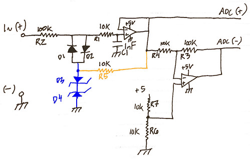

Let me know if I am understanding anything incorrectly, here is what I got:
R2 provides some input protection, and R1 sets the bias current.
D1 and D2 provide reverse polarity protection
D3 and D4 limits the input voltage to their zener value +.7V
R7 and R6 provides the common mode voltage as well as Vin (-) input
common mode voltage is set at 2.5 between R3 and R4
R4 provides return path for bias current
R3 - not sure of purpose. Balance the resistance of Vin(-) leg with Vin(+) leg?


Here's the things Id like to better understand:
What is the function of the 10K resistor R5?
What value of zeners to use? Around 4V?
It looks like there could possible be leakage current on the input through the diode string, and I'm not sure if that has much of an effect- is there any way to limit the leakage current? Or is it negligible?
D1 and D2 diodes- what would you suggest? Bav199? I think I have some BAT54 on hand already.. or would regular silicon diode be better?

I re-drew my interpretation of an effective version of the circuit, let me know if I've understood what you intended correctly
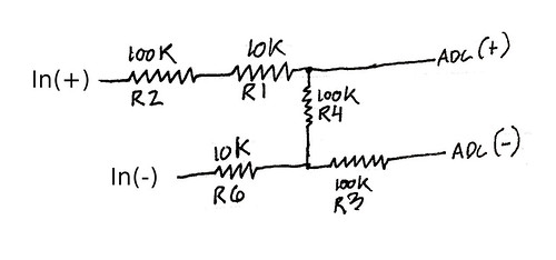


Offline Kleinstein

  • Super Contributor
  • ***
  • Posts: 14895
  • Country: de
Re: Need advice for ADC Buffer
« Reply #74 on: February 02, 2018, 10:04:26 am »
I think you still missed one key point: the negative side input thermal is not at the circuit ground, but at the same level as the ADC- input. There may be a series resistor for protection, though it might not be needed. They way you have drawn it errors from the 2nd OP would matter - they way I have drawn it, errors of the 2 nd OP would only shift the common mode voltage.

R2 together with D1-D4 is the main / coarse protection. R1 and the OP internal diodes towards the supply are a second level of protection. In addition R1 and C1 offer some filtering.  If more filtering is wanted additional caps at D1-D4 could be added. R5 helps to reduce the leakage current from the protection diodes. Leakage from D3/D4 can flow through R5. D1 and D2 only see a very small voltage and thus will show very low leakage (e.g. pA range even with more normal diodes).

The value of the Zeners would be something of about 3-4 V, so that with 2 forward diodes (e.g. D1 and D3) the voltage does no exceed the 5 V supply by much. For D1 and D2 a schottky diode is not the best choice, because of often higher leakage. BAV199 would be a good choice if really low leakage ( < 1 pA)  is needed, but due to the low voltage at the diodes more normal diodes like 1N4148 or 1N4001 could be used too. The diode leakage may matter a little near the ends (e.g. > 4.x V and < -4.x V), when the zeners start to conduct.

R3/R4 just set an inverting gain of -1 for the 2 nd OP. The value is kind of arbitrary and has nothing to do with impedance balancing. If so one would use the same value for R3,R4,R6,R7 - but it is not needed, as any offset around the 2 nd OP is not critical.


Share me

Digg  Facebook  SlashDot  Delicious  Technorati  Twitter  Google  Yahoo
Smf