Author Topic: Need advice for ADC Buffer  (Read 25200 times)

0 Members and 2 Guests are viewing this topic.

Offline CrossphasedTopic starter

  • Regular Contributor
  • *
  • Posts: 129
  • Country: us
Re: Need advice for ADC Buffer
« Reply #75 on: February 03, 2018, 09:02:24 am »
I think you still missed one key point: the negative side input thermal is not at the circuit ground, but at the same level as the ADC- input. There may be a series resistor for protection, though it might not be needed. They way you have drawn it errors from the 2nd OP would matter - they way I have drawn it, errors of the 2 nd OP would only shift the common mode voltage.

R2 together with D1-D4 is the main / coarse protection. R1 and the OP internal diodes towards the supply are a second level of protection. In addition R1 and C1 offer some filtering.  If more filtering is wanted additional caps at D1-D4 could be added. R5 helps to reduce the leakage current from the protection diodes. Leakage from D3/D4 can flow through R5. D1 and D2 only see a very small voltage and thus will show very low leakage (e.g. pA range even with more normal diodes).

The value of the Zeners would be something of about 3-4 V, so that with 2 forward diodes (e.g. D1 and D3) the voltage does no exceed the 5 V supply by much. For D1 and D2 a schottky diode is not the best choice, because of often higher leakage. BAV199 would be a good choice if really low leakage ( < 1 pA)  is needed, but due to the low voltage at the diodes more normal diodes like 1N4148 or 1N4001 could be used too. The diode leakage may matter a little near the ends (e.g. > 4.x V and < -4.x V), when the zeners start to conduct.

R3/R4 just set an inverting gain of -1 for the 2 nd OP. The value is kind of arbitrary and has nothing to do with impedance balancing. If so one would use the same value for R3,R4,R6,R7 - but it is not needed, as any offset around the 2 nd OP is not critical.

Hi Kleinstein,
As always thank you for your very educational reply!  I made the changes to match your original drawing, thanks for correcting me.


R5 totally makes sense now. Great idea to limit leakage current! The first OP drives R5 to be Vin - .7V, so there is very little voltage to cause leakage current. Below zener voltage +.7, any leakage current is supplied by OP1. So it looks like until the input voltage starts getting closer to 5V, Vc == Vb. Once the zener voltage is reached, and D3/D4 start drawing current, Vb drops a bit and D2 starts drawing more current off the input. Very clever I like it.  One questionthat pops into my mind looking at OP1- is there any relation between R1 and R5 being the same value? I imagine their values are somewhat flexible but I want to make sure I'm not overlooking something.

I'm having trouble picturing what the output of OP2 looks like. With an inverting OP, the output would normally be (-1)(Vin). But the virtual ground isnt 0 its 2.5V so I'm a little confused as to how one might calculate the output of OP2. For instance, what would ADC(-) be if nothing was applied to Vin+ or Vin- ?

Also, is there a situation where OP2 could start back feeding the source circuit? Its not something I'm concerned about for my application, but I'm curious if there is a situation where that might happen.

Other than that I think I'm ready to start putting this thing together. One more question on the final implementation- in the previous iteration, the noise of the chopper amps could be reduced by paralleling. Is that also the case with the Ad8552? I purchased a few of them, there's 2 op amps on each. I'm wondering if there's much to gain by paralleling them.

Lets see here...  what do you guys normally use for drawing schematics? I dont mind drawing by hand, but I dont see too many people doing it.

Cheers!


Offline Kleinstein

  • Super Contributor
  • ***
  • Posts: 14762
  • Country: de
Re: Need advice for ADC Buffer
« Reply #76 on: February 03, 2018, 10:41:22 am »
There is no relation between R1 and R5 - the same value is just coincidence. The inversion of OP2 is relative to the 2.5 V common mode point. So 1 V (relative to GND)  in is -1.5 V relative to 2.5 V and thus 2.5 + 1.5 = 4 V out. To reach this point one would need -3 V for the external source.  If there is no other connection from the ADC/amplifier circuit ground to the outside, there will be not current sourcing from OP2 to the external circuit. The driven "negative" terminal just needs isolated signal sources.

Paralleling OPs is working in principle, but it also increases input bias and current noise. So it usually is only done at the very low impedance / very low noise end, where you don't find a lower noise OP any more.  So it is possible to use two of the AD855x OPs in parallel (with resistors at the output to average). However there is a slight chance that 2 AZ OPs could cause trouble: if there internal chopper frequencies are close to each other there can be some inter-modulation and thus extra spurs to appear.

So I would avoid using two AZ Ops in parallel if not absolutely needed, e.g. at very low noise, when even an ADA4522 is not low enough in noise.

I would expect the ADC to have more noise than the AD8551 anyway, so the gain of an even lower noise amplifier is limited.
 

Offline CrossphasedTopic starter

  • Regular Contributor
  • *
  • Posts: 129
  • Country: us
Re: Need advice for ADC Buffer
« Reply #77 on: February 03, 2018, 10:57:34 pm »
The inversion of OP2 is relative to the 2.5 V common mode point. So 1 V (relative to GND)  in is -1.5 V relative to 2.5 V and thus 2.5 + 1.5 = 4 V out. To reach this point one would need -3 V for the external source.  If there is no other connection from the ADC/amplifier circuit ground to the outside, there will be not current sourcing from OP2 to the external circuit. The driven "negative" terminal just needs isolated signal sources.

Wow thanks, I think I finally get this circuit. I read what you wrote and kept looking at the circuit and thinking and finally understand how it works.


It looks like a voltage divider with the middle offset to +2.5

The 2.5 V offset- does that need to be a precision, stable value? By that I mean the 5 V divided down to 2.5, should the 5V be a reference voltage? My guess is it doesnt matter too much, because the ADC measures differential voltage and not single ended.


Damn I imagine things get pretty complicated if you have cascaded stages of these things!! For you as an experienced designer, do you look at a circuit like this and immediately understand whats going on? How long have you been doing this?


« Last Edit: February 03, 2018, 11:14:48 pm by Crossphased »
 

Offline Kleinstein

  • Super Contributor
  • ***
  • Posts: 14762
  • Country: de
Re: Need advice for ADC Buffer
« Reply #78 on: February 04, 2018, 08:50:49 am »
The 2.5 V level does not have to be accurate or very stable. So half the supply is Ok. The ADC should have a relatively good common mode suppression. Similar there is no need for higher accuracy for R3 and R4 and OP2.  For stability it might be a good idea to plan for a small cap in parallel to R3.

I have looked at a similar circuit just before this thread, so this was not just a quick Idea, but it took quite some thinking to get it. It is simple (just a few parts), but it is not that easy to understand.  For such a circuit it sometimes depends on the way it is drawn (your second drawing with divider makes it easy) - sometimes one gets the idea fast because one starts with the right hypothesis and sometimes it takes time as the first idea was wrong.

The protection part with the diodes and R5 is pretty much standard for the better DMMs and similar circuits.
 

Offline CrossphasedTopic starter

  • Regular Contributor
  • *
  • Posts: 129
  • Country: us
Re: Need advice for ADC Buffer
« Reply #79 on: April 08, 2018, 04:26:56 am »
I finally had time to return to this project. Life got in the way for a little while. I put the circuit together, and I'm getting really good performance out of the opamps. Those 8552 are great! I see a max of 1uV offset between OP input and ouput. Very impressive.

I'm having a bit of a problem with the protection circuit however. I'm seeing a significant voltage drop across the 100K input resistor. It's dropping ~4mV across it, which is also dropping the output by 4mV. That's not a large figure but its quite significant compared to the accuracy of the 8552. I did some probing and found the drop is due to current flowing through the diodes. If the bottom zener diode is disconnected, there is no more drop across the 100K input resistor.


The zeners are 3.3V, I cant remember the exact part number. The other diodes are 1N148. Is this behavior expected? And to be calibrated out? I'd like to improve this if possible. I experiments replacing the 100K with a 40K, and the 4mV drop was reduced to 1.5mV. I'd prefer to see it in the tens of uV however. What options do I have?

Here's what the implementation looks like below. Lt5400 were used for the 100K & 10K resistors- not for accuracy but to keep things compact. Using a leaded resistor instead of the LT5400 did not change the 4mV drop.

 
The following users thanked this post: Inverted18650

Offline Kleinstein

  • Super Contributor
  • ***
  • Posts: 14762
  • Country: de
Re: Need advice for ADC Buffer
« Reply #80 on: April 08, 2018, 09:09:27 am »
Some of the low voltage Zeners are not really good and have quite some leakage even well below there nominal voltage. So better quality zeners would be an option. A quick fix could be reducing R5  -  1  K should also be OK.

With a little more drop at the diodes it would make a difference using a low leakage diode like BAV199 here. As a dual diode in a SO23 case it could also make the circuit more compact.

Using the LT5400 for the resistors is not a good idea. Especially R2 should be able to withstand high voltages - the LT5400 is more like ESD sensitive and could easily be damaged. There is also no need for accurate resistors. Just plain thick film is OK: like size 1206 for R2 (or 2 or 3 0805 size in series), and 0805 or 0603 for the rest.

The ADC input likely should have some RC filtering at the input, like 100 Ohms / 500 nF
 - this could be well on the ADC board already.

Using an AD8552 is a bit odd: the second OP does not need to be an AZ type. Something very simple like LMV321 or MCP6001 would be good enough and would produce less supply noise.
 

Online nctnico

  • Super Contributor
  • ***
  • Posts: 27924
  • Country: nl
    • NCT Developments
Re: Need advice for ADC Buffer
« Reply #81 on: April 08, 2018, 10:15:30 am »
Protection on high impedance inputs is very hard to do. Zeners, TVS, etc all have very high leakage currents so they are useless for this purpose (and hence your circuit doesn't work). I usually use a relatively high value resistor in series and a capacitor to ground. The resistor limits the current into the chip's input ESD protection and the capacitor creates a low-pass filter. If you must use diodes then you should create a positive and negative supply to bias a couple of low leakage diodes (fdll333 for example) and use a TVS to deal with any nasty spike.
« Last Edit: April 08, 2018, 10:26:33 am by nctnico »
There are small lies, big lies and then there is what is on the screen of your oscilloscope.
 

Online David Hess

  • Super Contributor
  • ***
  • Posts: 17131
  • Country: us
  • DavidH
Re: Need advice for ADC Buffer
« Reply #82 on: April 08, 2018, 10:20:01 am »
R5 would normally have a much lower value.  It might be driven by another operational amplifier configured as a voltage follower buffering the output of the precision operational amplifier.

Even though a low voltage is across them, D1 and D2 need to be low leakage.  The collector-base junction of a small signal transistor like a 2N3904 works well.  So would LEDs painted black.
 

Offline CrossphasedTopic starter

  • Regular Contributor
  • *
  • Posts: 129
  • Country: us
Re: Need advice for ADC Buffer
« Reply #83 on: April 08, 2018, 08:49:05 pm »
Thank you all for your help and advice, I really appreciate it. I ordered the additional diodes to address the leaky zeners. I ordered both bav199 & 2N3904, I'm going to experiment with both. Also I like the idea of putting an addition voltage follower in to help keep the node at the top of the zeners as close to the input voltage as possible. I think the zeners I used were low leakage, but I'm not certain of it. Here's the two 3V3 zeners I have on hand:
https://www.digikey.com/product-detail/en/nexperia-usa-inc/BZX84-A3V3215/1727-5309-1-ND/2676785
https://www.digikey.com/product-detail/en/central-semiconductor-corp/CMOZ3V3-TR/CMOZ3V3CT-ND/5211381
One of them has 5uA reverse leakage and one has 2uA - does that sound acceptable?

So right now what I'm hearing from you guys is R5 being at 10K, drops some voltage across it which keeps the node at the top of the zeners a little below the input voltage. This in turn causes the 1N4148 to leak a bit, hence the extra current draw through the 100K input resistor - does that sound right? Would it ever be a good idea to place the diode protection string in front of the 100K resistor? I guess the diodes would have to sink more current then.

Also- the 3 uV drop across the 10K input resistor due to the bias current- is that going to be a constant value? By that I mean- will the bias current be equal across different input voltages? I'm wondering what the characteristics are for calibrating out the drop.

I was doing some reading last night on different voltage clamping methods and saw one that I hadn't seen before; using an opamp tolerant of higher input voltages than its power rails, to pull down the input if it gets above a reference value:

http://www.analog.com/en/technical-articles/op-amp-precision-positive-negative-clipper-using-lt6015-lt6016-lt6017.html

Thought it was really interesting but not really necessary for this application.

Regarding a different OP for buffering the common mode voltage, I dont have an extensive parts collection but here's some that might work, what do you guys think-
LTC6362
LTC6240
OPA227


Online nctnico

  • Super Contributor
  • ***
  • Posts: 27924
  • Country: nl
    • NCT Developments
Re: Need advice for ADC Buffer
« Reply #84 on: April 08, 2018, 09:01:49 pm »
Another thing to look out for is leakage in ceramic capacitors. You can easely get a few nA which is enough to get some extra voltage drop across a resistor. PET capacitors are your friend here.
There are small lies, big lies and then there is what is on the screen of your oscilloscope.
 

Offline Marco

  • Super Contributor
  • ***
  • Posts: 6947
  • Country: nl
Re: Need advice for ADC Buffer
« Reply #85 on: April 08, 2018, 09:21:58 pm »
Unless you need the bandwidth I'd just use a LTC2066 with >100K series resistance. Auto-zero, 5pA typical, can take 10 mA on the inputs using its internal (almost certainly bootstrapped) protection.
« Last Edit: April 08, 2018, 09:24:00 pm by Marco »
 

Offline CrossphasedTopic starter

  • Regular Contributor
  • *
  • Posts: 129
  • Country: us
Re: Need advice for ADC Buffer
« Reply #86 on: April 08, 2018, 09:22:39 pm »
Thanks nctnico,
I've been trying to stick with film caps in the signal path, but there is a ceramic on the input to the ADC. I've read piezo effects can cause noise with ceramic caps as well. Think I'll change it to a film cap. Are you partial to PET over polyester or polypropylene?
 

Offline CrossphasedTopic starter

  • Regular Contributor
  • *
  • Posts: 129
  • Country: us
Re: Need advice for ADC Buffer
« Reply #87 on: April 09, 2018, 03:31:26 pm »
Heya Kleinstein,
I'm getting rid of the 100K LT5400 block, but the 10K block should still be ok for dividing the reference voltage right? For the input 100K resistor, I ordered a few different values that could be wired in series to produce 100K- to help reduce ESD dangers. Got the 1206 size. (I hate soldering the 0805 and smaller!).

Also, yes I have 100 Ohm on the input to the ADC along with a 1uF capacitor. You suggested 1nF, is that just to provide the charge for the ADC bias current draw?

I put in my other response the zeners I have are supposed to have a leakage of 5uA and 2uA, is that a reasonable value or would you look for something lower leakage?

R5 is being changed to 1K, and I'm thinking about adding a voltage follower before it to help buffer the voltage a bit.

In commercial 6.5 digit or higher multimeters, what do they do to provide input protection and still maintain an accurate reading?
 

Offline CrossphasedTopic starter

  • Regular Contributor
  • *
  • Posts: 129
  • Country: us
Re: Need advice for ADC Buffer
« Reply #88 on: April 09, 2018, 03:39:27 pm »
Thanks David,
Good idea on adding the voltage follower, I'm going to add that. Just curious- what is the purpose of painting the LEDs black? Aesthetics or another reason?

Also I saw the concept of using jfet protection on the inputs in an application note- AN167. Found it interesting. A question though- if you are taking data with the ADC, how do you know when the jfets are current limiting and thus skewing the measurement?
 

Offline Kleinstein

  • Super Contributor
  • ***
  • Posts: 14762
  • Country: de
Re: Need advice for ADC Buffer
« Reply #89 on: April 09, 2018, 04:42:30 pm »
The bench top DMMs use a similar circuit, with low leakage diodes. Zener diodes at around 12-15 V often show less leakage below its nominal voltage than the 3.3 V ones. In addition there is often some kind of spark gap / MOV from before the 100 K resistor and another fusible resistor in front.

I don't think one will need an extra buffer: the leakage of the zener diodes is in the 10s of µA range and this is not a significant load for the OP, so no real need for an extra buffer. One might need one if the input amplifier is with gain.

Using such depletion mode FETs for protection should work, but the usual FETs are limited to about 800 V. So it might need to sets in series.  As it adds costs this would be something for high end meters where the noise from the 100 K (or similar) resistance does matter. An alternative might be a smaller resistor and a relay to turn of if the voltage is too high. However finding a suitable relay is not that easy.
 

Offline Marco

  • Super Contributor
  • ***
  • Posts: 6947
  • Country: nl
Re: Need advice for ADC Buffer
« Reply #90 on: April 09, 2018, 05:18:23 pm »
In commercial 6.5 digit or higher multimeters, what do they do to provide input protection and still maintain an accurate reading?

Varies wildly. AFAIR a 34401A simply has 100kOhm going into a JFET mux and a discrete JFET buffer (JFETs don't need protection other than current limiting). With (auto) calibration to correct for bias currents and offsets (and a relay to switch in a high voltage attenuator).
 

Online David Hess

  • Super Contributor
  • ***
  • Posts: 17131
  • Country: us
  • DavidH
Re: Need advice for ADC Buffer
« Reply #91 on: April 10, 2018, 07:02:51 pm »
Good idea on adding the voltage follower, I'm going to add that. Just curious- what is the purpose of painting the LEDs black? Aesthetics or another reason?

An LED painting black is a high forward voltage drop diode with very low leakage in the forward and reverse direction albeit with a relatively low peak inverse voltage rating which does not matter in this application.  If it was not painted black, then illumination would produce photocurrents which incidentally is a reason *not* to use glass packaged diodes in low leakage applications.  In the old days, glass low leakage diodes were painted black and if you scratched the paint off, the photocurrents would increase the leakage significantly.  This sometimes happened with metal-ceramic packaged transistors also.

Quote
Also I saw the concept of using jfet protection on the inputs in an application note- AN167. Found it interesting. A question though- if you are taking data with the ADC, how do you know when the jfets are current limiting and thus skewing the measurement?

You do not know unless you take steps to detect this condition.
 

Online David Hess

  • Super Contributor
  • ***
  • Posts: 17131
  • Country: us
  • DavidH
Re: Need advice for ADC Buffer
« Reply #92 on: April 10, 2018, 07:09:44 pm »
In commercial 6.5 digit or higher multimeters, what do they do to provide input protection and still maintain an accurate reading?

Varies wildly. AFAIR a 34401A simply has 100kOhm going into a JFET mux and a discrete JFET buffer (JFETs don't need protection other than current limiting). With (auto) calibration to correct for bias currents and offsets (and a relay to switch in a high voltage attenuator).

JFETs still need protection against reverse breakdown of their gate diode.  Their gate diode protects itself in the forward direction by conducting essentially forming half of the input protection network.  MOSFETs need protection both ways.

Since the maximum forward gate current of a MOSFET is relatively low, external protection may still be needed.

As far as bench multimeters, the input protection networks are like the ones discussed here.  A series impedance and clamp is used before a high input impedance buffer.  If the input current is in the picoamp range, then the high impedance of the series network can limit the input current to safe levels even at high voltages while preserving precision.


Offline Marco

  • Super Contributor
  • ***
  • Posts: 6947
  • Country: nl
Re: Need advice for ADC Buffer
« Reply #93 on: April 10, 2018, 07:29:16 pm »
It's a PN junction, it will non destructively avalanche if you limit current.
 

Online David Hess

  • Super Contributor
  • ***
  • Posts: 17131
  • Country: us
  • DavidH
Re: Need advice for ADC Buffer
« Reply #94 on: April 11, 2018, 12:37:32 am »
It's a PN junction, it will non destructively avalanche if you limit current.

In my experience, JFETs just die under conditions where the gate diode goes into reverse breakdown even when the current is limited.  If the JFET is not destroyed, then I suspect the damage from hot carriers will ruin the gate leakage and alter the threshold voltage.
 

Offline Marco

  • Super Contributor
  • ***
  • Posts: 6947
  • Country: nl
Re: Need advice for ADC Buffer
« Reply #95 on: April 11, 2018, 01:29:22 am »
Be that as it may, they have no discrete protection. Only a PCB spark gap, a couple of resistors and then directly into the mux ... if they have any bootstrapped protection it's in there.

Looking again, I do notice now they have a pre-amp in the same IC to precharge the JFET buffer during autocalibration.
 

Online David Hess

  • Super Contributor
  • ***
  • Posts: 17131
  • Country: us
  • DavidH
Re: Need advice for ADC Buffer
« Reply #96 on: April 11, 2018, 01:34:25 am »
Be that as it may, they have no discrete protection. Only a PCB spark gap, a couple of resistors and then directly into the mux ... if they have any bootstrapped protection it's in there.

It is likely.  And one of the more common diodes used to protect a JFET gate from reverse breakdown is the gate of another of the same JFET since it will have the right leakage characteristics.

JFETs with guaranteed leakage are less expensive than guaranteed diodes or transistors unless you grade them yourself.
 

Offline CrossphasedTopic starter

  • Regular Contributor
  • *
  • Posts: 129
  • Country: us
Re: Need advice for ADC Buffer
« Reply #97 on: April 13, 2018, 05:07:11 am »
The bench top DMMs use a similar circuit, with low leakage diodes. Zener diodes at around 12-15 V often show less leakage below its nominal voltage than the 3.3 V ones. In addition there is often some kind of spark gap / MOV from before the 100 K resistor and another fusible resistor in front.

I was doing some reading on transient protection & tvs diodes. It looks like when clamping to a higher voltage, say 30V, there is much less leakage current- around 1 uA. Would it ever make sense to use this kind of transient protection in front of the 100K input resistor to protect against ESD/overvoltage, which would then allow using a smaller resistor than 100K for current limiting? Say a tvs diode that clamps at 30V, then you only need to use a 30K input resistor?

For instance I was checking out this family of transient suppressors: http://www.vishay.com/docs/85881/smf5v0atosmf58a.pdf
they have .1 uA leakage current for clamp voltages as low as 9V


Just curious thats all!
« Last Edit: April 13, 2018, 05:35:54 am by Crossphased »
 

Offline CrossphasedTopic starter

  • Regular Contributor
  • *
  • Posts: 129
  • Country: us
Re: Need advice for ADC Buffer
« Reply #98 on: April 13, 2018, 05:14:53 am »
Some of the low voltage Zeners are not really good and have quite some leakage even well below there nominal voltage. So better quality zeners would be an option. A quick fix could be reducing R5  -  1  K should also be OK.

While waiting for parts to arrive from DigiKey, I did as you suggested and lowered R5 to 1K. Results improved considerably, thank you! The voltage drop across the 1K is now 16 mV, so less leakage current through the diode string, and less offset voltage at the output. The difference between input and output is now down to ~60 uV, much better!

With the BAV199 replacing the 1N148 diodes, would you expect the leakage current to drop significantly, and lower the discrepancy between input and output further?

As always, thank you for your experience and guidance
« Last Edit: April 13, 2018, 05:17:23 am by Crossphased »
 

Offline CrossphasedTopic starter

  • Regular Contributor
  • *
  • Posts: 129
  • Country: us
Re: Need advice for ADC Buffer
« Reply #99 on: June 24, 2018, 07:13:55 pm »
Hey friends,

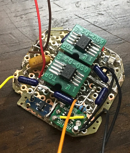
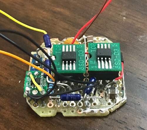
I've had some time to return to this project. The circuit was put together with a value of 1K for R5, BAV199 diodes, 3.3V Zeners, and MCP6002. Performance is quite good and I'm pleased.


I did some interesting experiments over the weekend involving temperature coefficient. I've always read about temperature coefficient of passives, and I became curious about what that looks like in the real world. So an experiment was done.

A battery (AA) was used to provide a stable input voltage. The output voltage was measured with a 6.5 digit voltmeter (SDM3065). To test, a straw was used, air from mouth blown over individual components, one at a time, response in output voltage noted, and how long it took to recover to the initial voltage. All resistors are from the same manufacturer, and same series.
Schematic as reference:


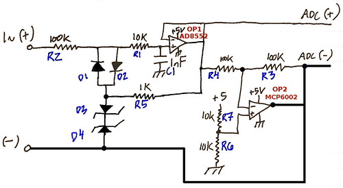
1. D1+D2(Single package): output dropped by 3 milliVolts. Took 5 minutes to recover to initial value.
2. R2: output voltage only dropped 6 microVolts, and recovered to initial value in 20 seconds.
3. R1: output voltage dropped 3 milliVolts, took 2 minutes to recover.
4. D3,D4: Output dropped by 8 milliVolts, took 5 minutes to recover
5. R4: Output dropped by 30 milliVolts, took 3 minutes to recover
6. R3: Output dropped by 50 milliVolts, took 3 minutes to recover
7. R7:Output dropped 20 milliVolts, took 5 minutes to recover
8. OP1 (8552): Output dropped 4 milliVolts, 4 minutes to recover
9. OP2(MCP6002): Output dropped 3 milliVolts, took 3 minutes to recover

Next step is to put this together with the ADC
« Last Edit: June 24, 2018, 07:17:51 pm by Crossphased »


Share me

Digg  Facebook  SlashDot  Delicious  Technorati  Twitter  Google  Yahoo
Smf