Author Topic: Memory - die pictures  (Read 7326 times)

0 Members and 1 Guest are viewing this topic.

Online RoGeorge

  • Super Contributor
  • ***
  • Posts: 6515
  • Country: ro
Re: Memory - die pictures
« Reply #25 on: May 19, 2024, 11:37:11 am »
If it is so, then yo got yourself a 4 Megapixel UV camera.  Cool!  8)
Should also work as a 4MP X-ray camera.  :scared:

First, program all the EEPROM with zero's, then expose it to X-rays for a while, then read back the memory.  X-rays energy is above the UV light, so the exposing time won't be that slow as when erasing the cells with UV.  Too bad the EPROMs do not have some "service/debug" mode to allow analog reading of each cell instead of just 0/1.  That would have turned any big enough EPROM into a high resolution X-ray film, but in silicon and reusable a few times.  :D

Offline NoopyTopic starter

  • Super Contributor
  • ***
  • Posts: 1848
  • Country: de
    • Richis-Lab
Re: Memory - die pictures
« Reply #26 on: May 19, 2024, 11:42:25 am »
That's an interesting idea. Indeed, Black&White should work.  :-+

But you will need some good quartz lenses.  :-/O
« Last Edit: May 19, 2024, 12:11:09 pm by Noopy »
 

Offline NoopyTopic starter

  • Super Contributor
  • ***
  • Posts: 1848
  • Country: de
    • Richis-Lab
Re: Memory - die pictures
« Reply #27 on: July 15, 2024, 03:22:29 am »


The FM28V100 is an FRAM with the same specifications as the FM24V10 (https://www.richis-lab.de/RAM01.htm). The only difference is the parallel interface of the FM28V100. It has 16 address inputs and an 8-bit wide data interface. The FM24V10, on the other hand, is available with an SPI or I2C interface.


Apparently, the FM28V100 uses the same design as the FM24V10. This could already be surmised, as the die has many more bondpads than are used in the FM24V10.

However, the design of the die is not completely identical. The FM28V100 has an additional metal layer, but this is only filled with a dummy structure.


Dummy structures are usually added so that the layers can be processed as evenly as possible. If layers are very inhomogeneous, it can happen, for example, that a grinding process has not yet removed enough material at one point, while at another point it has already penetrated too deep into the structures. In this case, however, the top metal layer is not utilised at all. It was not present at all in FM24V10. It remains unclear what purpose the dummy structures fulfil.


Apart from the dummy structure, there is no superficial difference between the FM28V100 and the FM24V10. However, there is a small update in the top right-hand corner. This shows the year 2016, while the FM24V10 shows the year 2008.


https://www.richis-lab.de/ROM09.htm

 :-/O
 
The following users thanked this post: RoGeorge

Offline NoopyTopic starter

  • Super Contributor
  • ***
  • Posts: 1848
  • Country: de
    • Richis-Lab
Re: Memory - die pictures
« Reply #28 on: August 02, 2024, 03:49:41 am »


I have some more pictures showing details of the U2164!
The 64kBit DRAM U2164 shown here was manufactured in March 1988 at the "Zentrum für Mikroelektronik Dresden". A lot of background information about the U2164 can be found in the documentation of the Tesla MHB4164, which also contains a U2164: https://www.richis-lab.de/RAM02.htm


As with the Tesla MHB4164, the dimensions of the die are 7,0mm x 3,4mm.
This image is also available in a higher resolution: https://www.richis-lab.de/images/RAM/07x02XL.jpg (36MB)


On the left edge is the designation and the number 5, which most likely refers to the revision of the design.


The structures can be recognised a little better in this picture. Due to the high density, the area of the memory cells still remains unclear.


The carrier on which the die is located is visible on the side of the package. The voltage generated by the integrated charge pump can be measured there. On another U2164 (date code March 1989) this voltage is -1,7V. The potential is applied to the substrate via the carrier and thus optimises the threshold of the integrated transistors.


Each of the eight memory blocks in the U2164 has a reserve row and two reserve columns. This increases the yield considerably, as it is possible to switch to these reserve areas in the event of production errors in the memory. Switching takes place via an area on the right-hand edge of the die. There are 32 and 36 fuses located there. To trigger the fuses, the area is obviously supplied via three testpads.


Large transistors can be seen above the fuses, which allow the trigger current to flow. The necessary fuses are apparently selected via the addressing interface. The area of the fuses looks a little unclean because the passivation layer has been omitted in this area. This is necessary so that triggering a fuse leads to a safe interruption of the connection. It also ensures that triggering does not cause major damage to the surrounding passivation layer.

How the addresses are redirected to the reserve areas remains unclear. Usually the address decoding is changed for this purpose. Modifying the addressing does not allow completely arbitrary replacement of memory cells, but it is often sufficient to hide all defective cells.


https://www.richis-lab.de/RAM07.htm

 :-/O
 
The following users thanked this post: T3sl4co1l, RoGeorge

Offline NoopyTopic starter

  • Super Contributor
  • ***
  • Posts: 1848
  • Country: de
    • Richis-Lab
Re: Memory - die pictures
« Reply #29 on: August 05, 2024, 02:49:06 pm »


The U2164 shown here was manufactured in April 1987.


The large die requires a lot of space in the DIL-16 package.


On the die you can see some dirt and artefacts. This picture is also available in a higher resolution: https://www.richis-lab.de/images/RAM/08x02XL.jpg (48MB)


The die is coated with a protective layer, which partly explains the dirt. Particles usually adhere very strongly to such protective layers. However, a not inconsiderable proportion of the contamination must have already been on the die before the package was opened.

Coatings are not primarily used to protect memory modules from contamination, but rather to shield them from radioactive radiation. This means that alpha particles from the housing material cannot affect the memory cells.


There is a dark spot on the upper edge of the die, under which one would suspect an electrical defect. However, it only appears to be soiling in the potting material.


The die marking documents that this is the fourth revision of the U2164. The Tesla MHB4164 (April 1990) and the previously documented U2164 (March 1988) are labelled revision 5, which means that between April 1987 and March 1988 the revision was changed from revision 4 to revision 5.


It can be seen that revision 5 of the U2164, measuring 7,1mm x 3,4mm, is significantly smaller than the revision 4 used here, which measures 8,2mm x 3,8mm. Such a significant reduction in surface area cannot be achieved with minor optimisations. All structures were apparently reduced in size for revision 5. However, the functional blocks appear to have the same electrical structure apart from minor details.


The protective layer somewhat disturbs the view on the structures. However, the capacitors that store the data can now be recognised in the memory area.


The details of the structures show that the memory is not built exactly as described in Radio Fernsehen Elektronik 08/1989. When analysing the U2164 in the Tesla MHB4164 (https://www.richis-lab.de/RAM02.htm), it had to be assumed that the documentation depicted reality exactly. The mode of operation is shown correctly, but the superimposition of the structures has been simplified. The very dense arrangement in the memory array means that the word lines are not only routed over the areas where they are building the selection transistors. They also lie on the areas that represent the capacities.

At first glance, it appears that this additional overlay could have an undesirable effect on the memory cells. The image of the cross-section provides clarity. The storage capacities arise between the substrate and the first polysilicon layer, whereby the first polysilicon layer represents the reference potential. If there is a line in the second polysilicon layer above this first polysilicon layer, this has no relevant influence on the storage capacity.


A major change has been made in the area of the charge pump, which sinks the substrate to a negative potential. The same circuit parts can be recognised, but in revision 5 (below) a lot has been omitted.

Apparently, this area was not only used to generate the negative substrate voltage. In revision 5, a line leads to various elements in the left part of the die. In revision 4, the beginning of this line is present, but it leads to an open end.


The circuit section for switching to reserve areas is constructed in the same way in revision 4 as in revision 5. The recesses in the passivation layer are even more clearly recognisable here. No fuse was triggered. The memory appears to have been faultless.


This component is defective. Without adressing, it draws more than 100mA. An infrared camera with a macro lens makes it possible to identify the area with the greatest heat development. This is not necessarily the location of the fault. The heat development can be a subsequent reaction. However, such an image can help to identify faults.


If the thermal image is superimposed, it becomes clear that the greatest heat development occurs in the area of the first bondpad. However, no obvious damage can be recognised in this area.


Here you can see another U2164 in a ceramic case. It was produced at the same time as the upper U2164.


The protective coating appears even more soiled here than in the first U2164. This picture is also available in a higher resolution: https://www.richis-lab.de/images/RAM/09x03XL.jpg (47MB)


Here, too, a small area of the protective coating is very dark.


This U2164 was obviously not perfect. Here you can see some triggered fuses.


https://www.richis-lab.de/RAM08.htm

 :-/O
 
The following users thanked this post: RoGeorge, iMo

Offline iMo

  • Super Contributor
  • ***
  • Posts: 4978
  • Country: cv
Re: Memory - die pictures
« Reply #30 on: August 05, 2024, 03:12:33 pm »
Afaik those TESLA MHB4116, MHB4164 and later on MHB41256 (not sure the 256k one went into full production though) were produced in the famous spa town Piestany (Slovakia today) on a production equipment purchased and nmos/cmos technology licensed from Toshiba, 4um and perhaps 1um or 2um at the end of its existence (starting memory production from early 80ties till early 90ties)..
« Last Edit: August 11, 2024, 07:33:14 am by iMo »
 

Offline NoopyTopic starter

  • Super Contributor
  • ***
  • Posts: 1848
  • Country: de
    • Richis-Lab
Re: Memory - die pictures
« Reply #31 on: August 05, 2024, 03:56:06 pm »
It seems that at least for some time the MHB4164 was a U2164 and was packaged in Erfurt.

The geometries are typical for Erfurt.

https://www.richis-lab.de/RAM02.htm

Offline iMo

  • Super Contributor
  • ***
  • Posts: 4978
  • Country: cv
Re: Memory - die pictures
« Reply #32 on: August 05, 2024, 04:04:12 pm »
Yep, it is possible, in the time of east european Comecon they were packaging chips cross border happily. Sometimes the chips from the west as well..
 

Offline NoopyTopic starter

  • Super Contributor
  • ***
  • Posts: 1848
  • Country: de
    • Richis-Lab
Re: Memory - die pictures
« Reply #33 on: August 05, 2024, 04:11:19 pm »
Well cooperation makes sense. Other projects were less reasonable:
The DDR and the SU both independently made a copy of the MicroVAX II CPU.  ;D

Offline iMo

  • Super Contributor
  • ***
  • Posts: 4978
  • Country: cv
Re: Memory - die pictures
« Reply #34 on: August 05, 2024, 05:05:22 pm »
Btw. - a less known company Everspin sent me some 10+y back a 4Mbit MRAM sample (I think the MR20H40, but I cannot find it in my junk box anymore). Would be interesting to see that chip too - as that technology is quite mysterious..  :o
« Last Edit: August 05, 2024, 05:07:00 pm by iMo »
 

Offline NoopyTopic starter

  • Super Contributor
  • ***
  • Posts: 1848
  • Country: de
    • Richis-Lab
Re: Memory - die pictures
« Reply #35 on: August 05, 2024, 07:21:57 pm »
I have heard of these MRAM devices. Unfortunately I´m pretty sure you can´t see very much in a 4Mbit device. But if you want me to take a closer look...  ;) ;D

Offline NoopyTopic starter

  • Super Contributor
  • ***
  • Posts: 1848
  • Country: de
    • Richis-Lab
Re: Memory - die pictures
« Reply #36 on: August 08, 2024, 04:03:42 am »


A small update for the U2164: Here you can see the dummy cells that are used to read the memory cells.


https://www.richis-lab.de/RAM07.htm#Dummy

 :-/O
 
The following users thanked this post: RoGeorge

Offline NoopyTopic starter

  • Super Contributor
  • ***
  • Posts: 1848
  • Country: de
    • Richis-Lab
Re: Memory - die pictures
« Reply #37 on: August 11, 2024, 04:48:03 am »


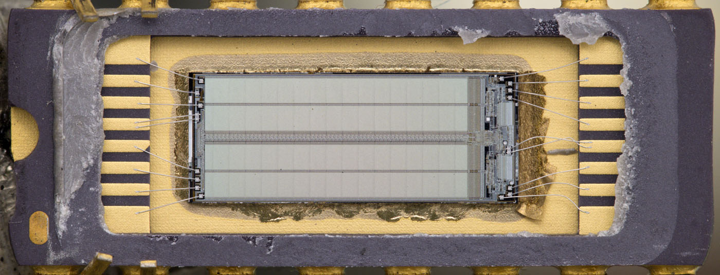
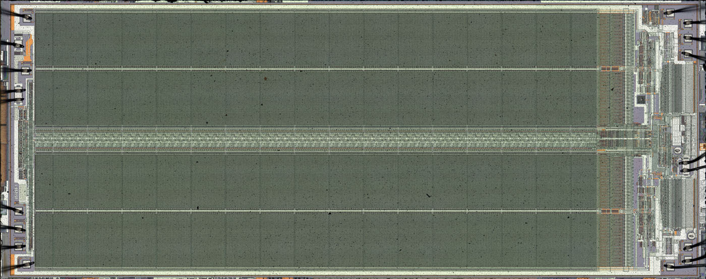
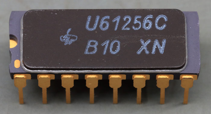
The 256kBit DRAM U61256 was developed at the Zentrum für Mikroelektronik in Dresden. It was the largest mass-produced RAM in the GDR. The subsequent 1MBit memory U61000 was only produced in a small series. The characters XN indicate production in November 1989.

The numbers 10 stand for the first selection type, which allowed access times of 100ns. This was followed by selection type 08, which was specified with 80ns. The basic type (12) offers access times of 120ns, the slowest bin (15) has an access time of 150ns.
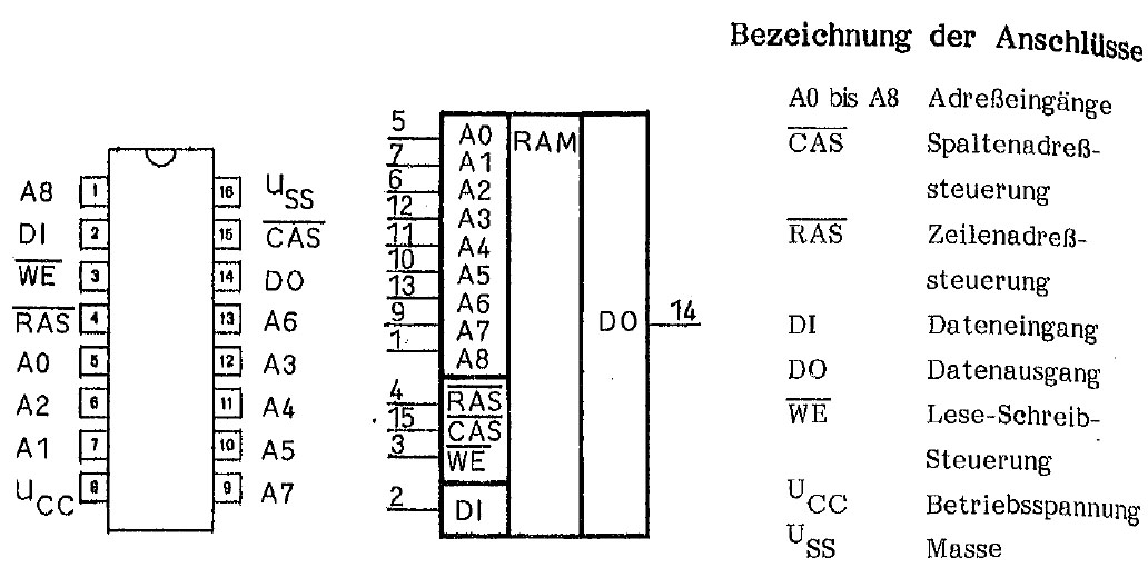
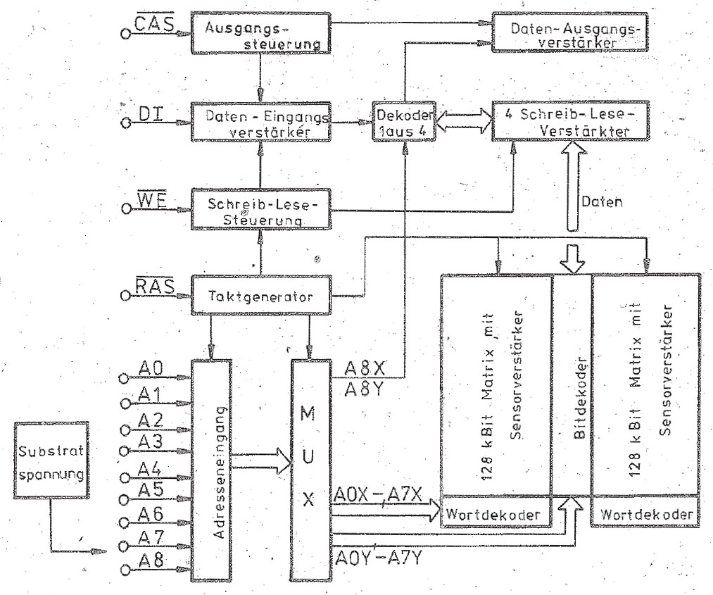


The datasheet shows the structure and function of the U61256. 8 bits of the 9-bit wide addressing interface are first decoded for row selection and then for column selection. The memory consists of two 128kBit areas which output the information of four cells simultaneously when reading data. The ninth bit of the addressing interface, which is also evaluated twice, controls the selection of one of these four cells. The data output in the top right-hand corner is missing in the block diagram.
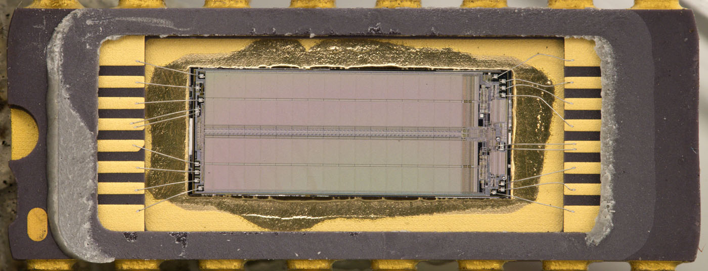


The size of the die is 9,6mm x 3,8mm. Each supply potentials is routed to the die with two bondwires.
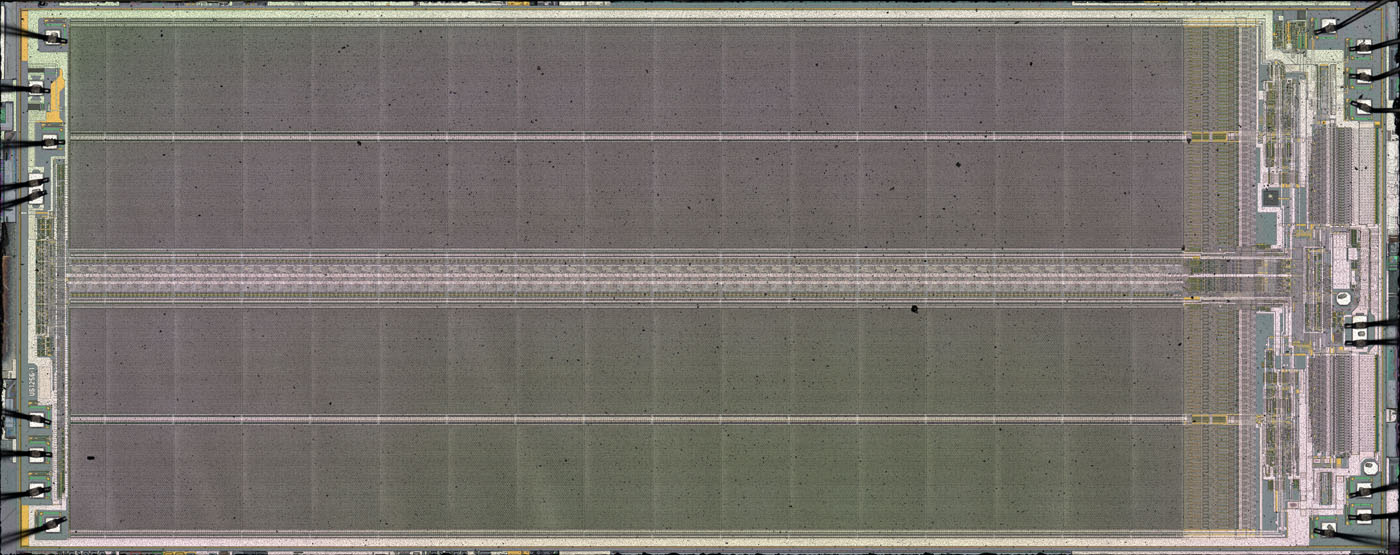


The image of this is also available in a higher resolution: https://www.richis-lab.de/images/RAM/10x03XL.jpg (67MB)
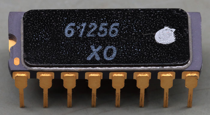


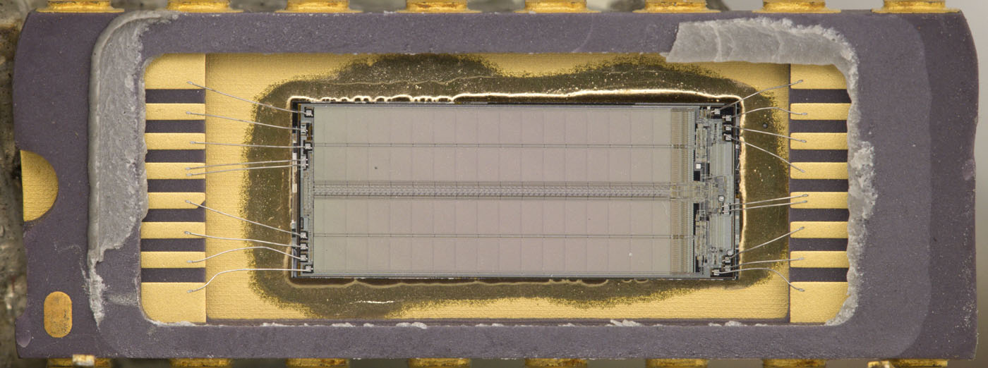
Here you can see another U61256. The bin marking is missing on this component. XO indicates production in October 1989.

The image of this part is also available in a higher resolution: https://www.richis-lab.de/images/RAM/11x03XL.jpg (71MB)
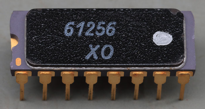


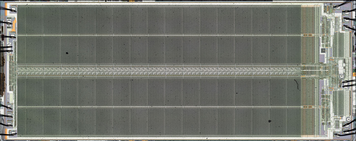
The third U61256 appears to come from the same batch as the second.

The image of this part is also available in a higher resolution: https://www.richis-lab.de/images/RAM/12x03XL.jpg (71MB)


All three dies are labelled U61256-1. The number 1 probably indicates the first revision of the design. Fittingly, I can´t see a difference in the three parts.
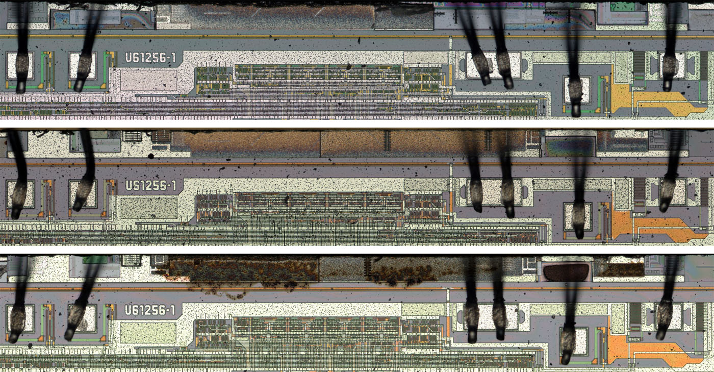


The left-hand edge appears to have had some imperfections during production. The third part shows soiling or signs of corrosion that extend to the first active structures.


On the upper edge you can see some masks.
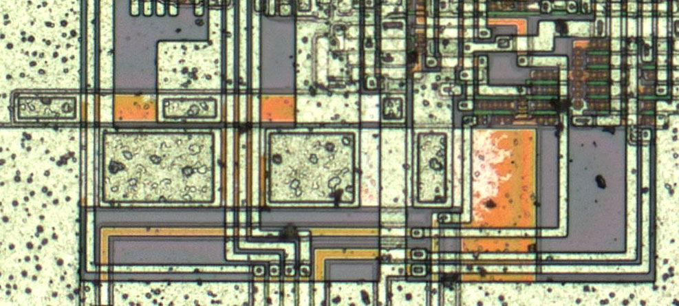


The metal layer appears to have penetrated from the contacts into the polysilicon layer in many areas. The effect can be found in all three parts. The section shown here is from the third part.
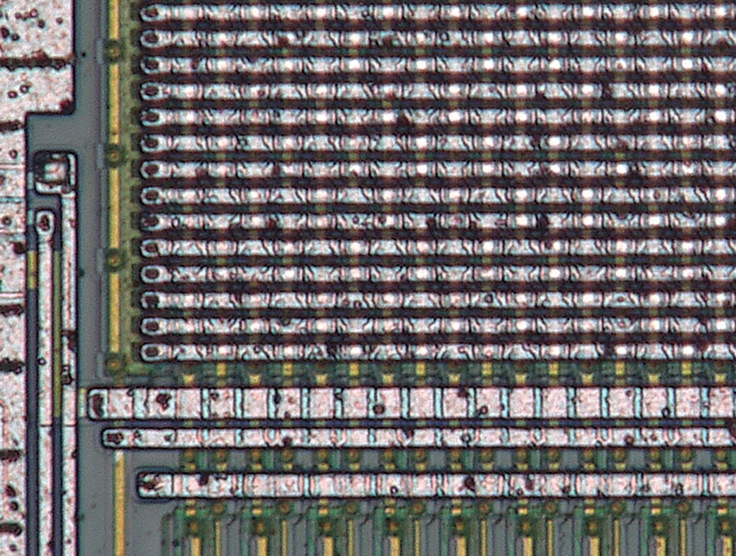


The memory cells are too small and there are too many layers on top of each other to be able to clearly recognise the structure. The surface structure of the metal layer appears to show capacitor geometries similar to those in the U2164.

As in the U2164, line selection in the U61256 also takes place laterally and data evaluation is placed at the lower or upper edge of the storage areas. In contrast to the U2164, however, the lines in the metal layer run horizontally rather than vertically.
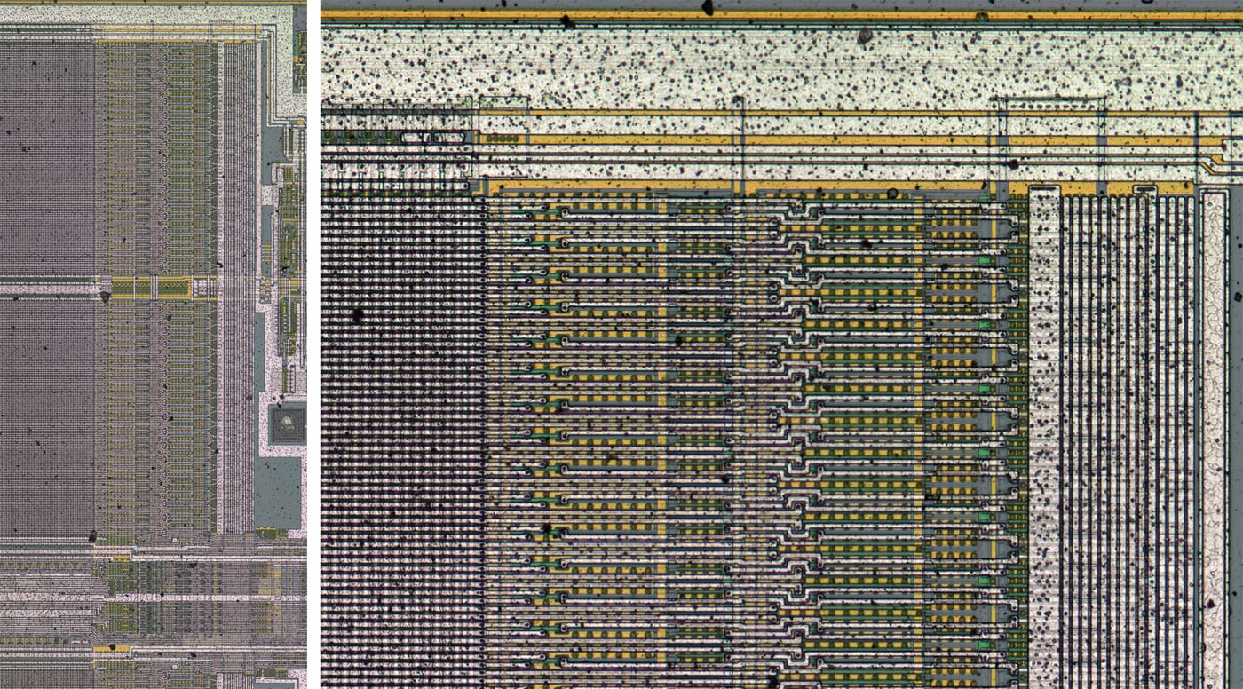


The memory area only has line drivers on the right-hand side. Correspondingly large driver transistors are integrated there in order to be able to represent the necessary charging current. This could also be an explanation for the horizontal lines in the metal layer. The metal layer has a lower impedance than the polysilicon layer.
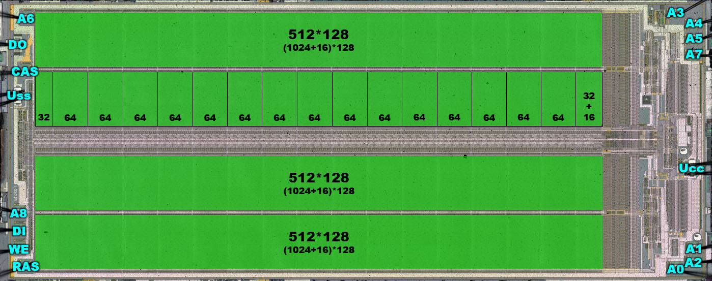


In the block diagram, the memory area is divided into two parts. The upper and lower blocks each consist of two areas. Each of these areas contains 15 segments, from each of which 64 lines lead out of the area. There are 32 lines at the beginning and 32 at the end. This results in a total of 256.000 memory cells. There are 16 additional columns on the right-hand edge. Apparently, the memory has 16 reserve columns, i.e. 8.192 additional memory cells, to compensate for production errors.


Here you can see the structures that run through the two large storage areas. The supply lines are relatively massive. Perhaps they are used to preload the columns before the memory cells are read.
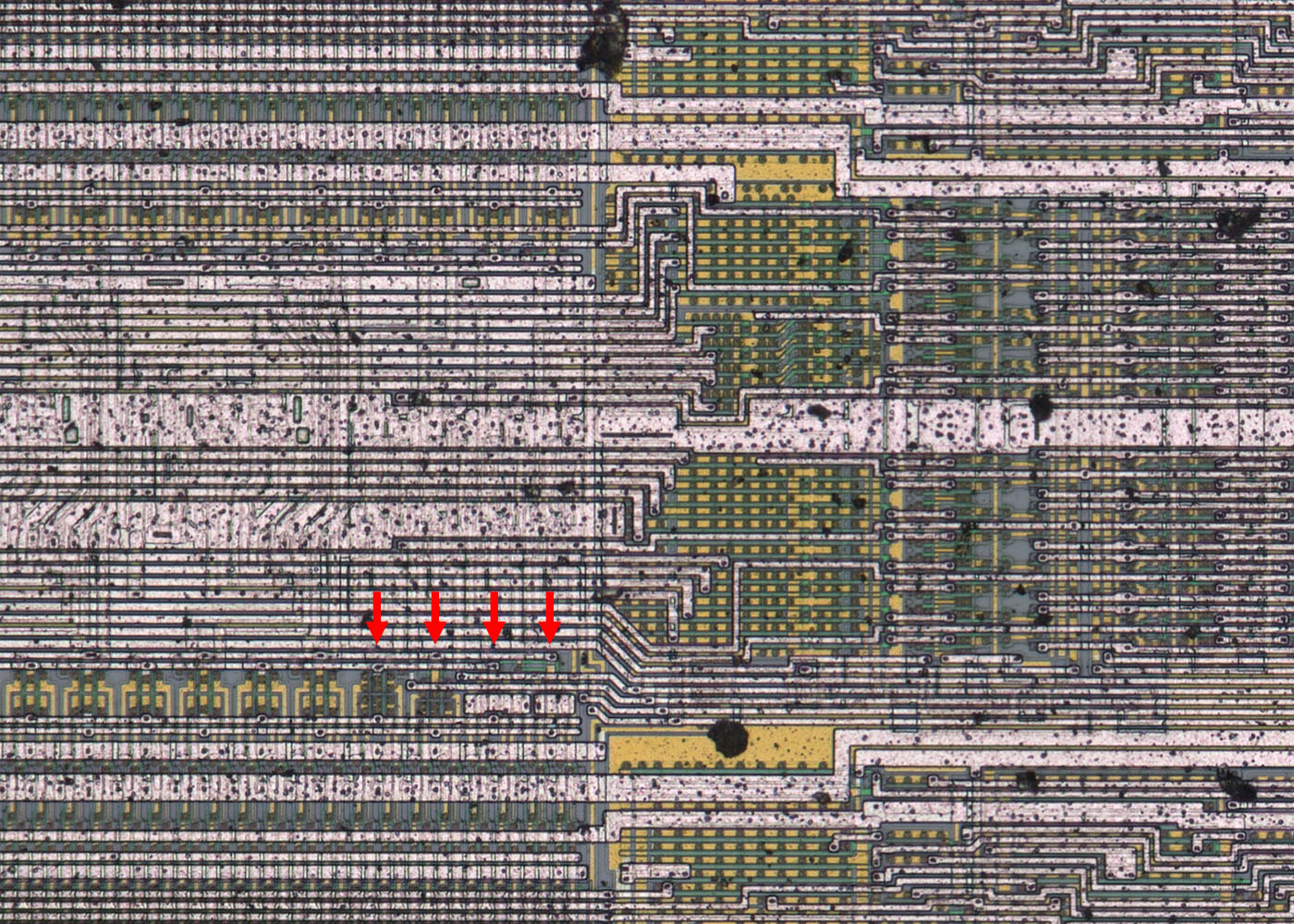


Even if the exact structures of the column selection cannot be recognised, some functions can be surmised. Two times eight lines run horizontally between the two large memory blocks. These are most probably the address lines for the two memory blocks. Four lines run somewhat shielded from this in the centre, which then certainly transmit the four memory contents readout.

The fact that the 16 columns on the right are the reserve columns can also be seen here (red arrows). The first four blocks, which read out four columns each, are constructed and contacted differently. Five additional control lines are routed to this area.


The circuit that enables the reserve columns to be looped into the address range is integrated on the right-hand edge. There are two times 36 fuses near the edge of the die for this purpose. The triggering is apparently similar to that of the U2164. Two testpads are integrated, one of which transmits the triggering current.


The triggered fuses can be easily recognised. The fuses are thin polysilicon strips. Some fuses were triggered in all three parts. Apparently there were defective cells in all three parts.
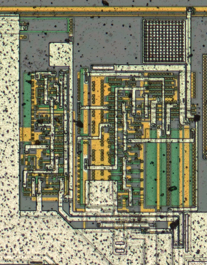


The bias voltage generation is located in the top right-hand corner of the die, which places the substrate at a negative potential. In the upper area, the circuit contacts the frame structure. This potential is also used in some parts of the circuit.

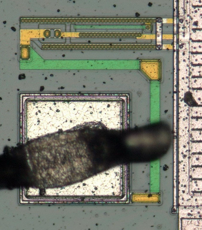
In addition to the two testpads for triggering the fuses, there are two further testpads on the die. It is interesting to note that the surface of these testpads has a different structure. It could be that two types of testpads were used depending on the application. The testpads of the fuses are always contacted during production. The bias voltage probably only rarely needs to be measured. This testpad is also significantly smaller. The function of the fourth testpad remains unclear. Although its surface is structured in the same way as the bias voltage generation testpad, it was contacted for all three components.


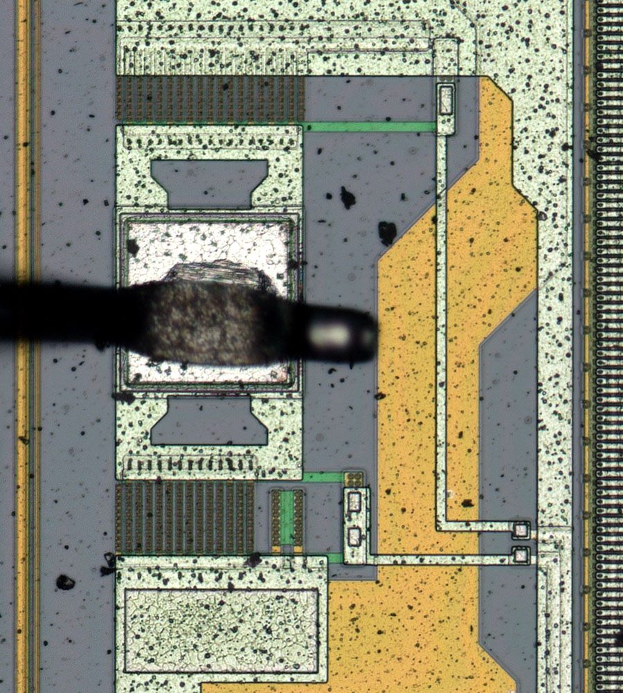
Here you can see an input protection circuit. It probably works in a similar way to the input protection circuit in the U2164. The two long, green elements are resistors for current limitation. In the upper area, two elements are surrounded by strips that are connected to the ground potential. The first element is probably a diode. The second element is a grounded gate NMOS.


The push-pull output stage of the data output is very easy to recognise.


https://www.richis-lab.de/RAM09.htm

 :-/O
 
The following users thanked this post: RoGeorge, iMo

Offline iMo

  • Super Contributor
  • ***
  • Posts: 4978
  • Country: cv
Re: Memory - die pictures
« Reply #38 on: August 11, 2024, 07:35:53 am »
Quote
This results in a total of 256.000 memory cells. There are 16 additional columns on the right-hand edge. Apparently, the memory has 16 reserve columns, i.e. 8.192 additional memory cells, to compensate for production errors.
I wonder what was the typical yield at that time in the Dresden fab?

PS: @Noopy: a high time to acquire an electron beam microscope (as a minimum) :)

TSMC starts construction on its first European chip plant in Dresden, Germany, marking a $10 billion investment to boost the semiconductor industry.

Quote
..The ground-breaking ceremony, scheduled for August 20, 2024, will initiate a project expected to be operational by late 2027. The facility will focus on producing 28nm, 22nm, and 16/12nm nodes, critical for various applications from automotive to industrial equipment​.

https://manufacturing-today.com/news/tsmc-commences-10-billion-semiconductor-plant-project-in-germany/

« Last Edit: August 11, 2024, 08:25:05 am by iMo »
 

Offline NoopyTopic starter

  • Super Contributor
  • ***
  • Posts: 1848
  • Country: de
    • Richis-Lab
Re: Memory - die pictures
« Reply #39 on: August 11, 2024, 08:01:05 am »
Quote
This results in a total of 256.000 memory cells. There are 16 additional columns on the right-hand edge. Apparently, the memory has 16 reserve columns, i.e. 8.192 additional memory cells, to compensate for production errors.
I wonder what was the typical yield at that time in the Dresden fab?

You don´t find very much information about the U61256. The situation is much better for the U2164 and the U61000.
The U2164 yield was increased starting from 6% in 1987 to 50% in 1988. It is said that there was a cooparation with Toshiba which helped a lot. (Kampfauftrag
Mikrochip, Olaf Klenke)

It seems >10% was considered as not bad.  ;D


PS: @Noopy: a high time to acquire an electron beam microscope (as a minimum) :)

I don´t want to own one myself I just would love to have unlimited access to one.  ;D
« Last Edit: August 11, 2024, 08:03:22 am by Noopy »
 
The following users thanked this post: iMo

Online magic

  • Super Contributor
  • ***
  • Posts: 6980
  • Country: pl
Re: Memory - die pictures
« Reply #40 on: August 11, 2024, 09:28:02 am »
You can still go further with optical, I think 1980s technology should be within reach.

In order to at least pretend that I'm staying on topic, below is a memory array (probably SRAM because there was another, larger one which would be the program memory) of an unknown low cost MCU from tenx technology which I extracted from a bicycle speed meter made in mid 2000s. I included bond pads for size reference, these are almost always 100×100 micron on all chips. Image scale is 200nm/px, determined by dividing measured overall die size by pixel count.

This image was assembled from many smaller frames and not all of them were in perfect focus, but you can see that pretty fine details are resolvable with an ordinary 40x0.65 objective. DoF becomes a serious pain, though, and focusing on the low layers tends to blur the upper metal somewhat. You could still get twice the resolution by employing oil immersion, but there is no way the results would be usable without focus stacking.
 

Offline NoopyTopic starter

  • Super Contributor
  • ***
  • Posts: 1848
  • Country: de
    • Richis-Lab
Re: Memory - die pictures
« Reply #41 on: August 11, 2024, 10:44:21 am »
A lot is possible with the right equipment and some automation. It helps a lot if you have some knowledge in optics and programming. This french guy here produces some really nice pictures including "interactive" focus stacking: https://ic.onidev.fr/en/die/multifocus_panoramas.html
 
The following users thanked this post: magic


Share me

Digg  Facebook  SlashDot  Delicious  Technorati  Twitter  Google  Yahoo
Smf