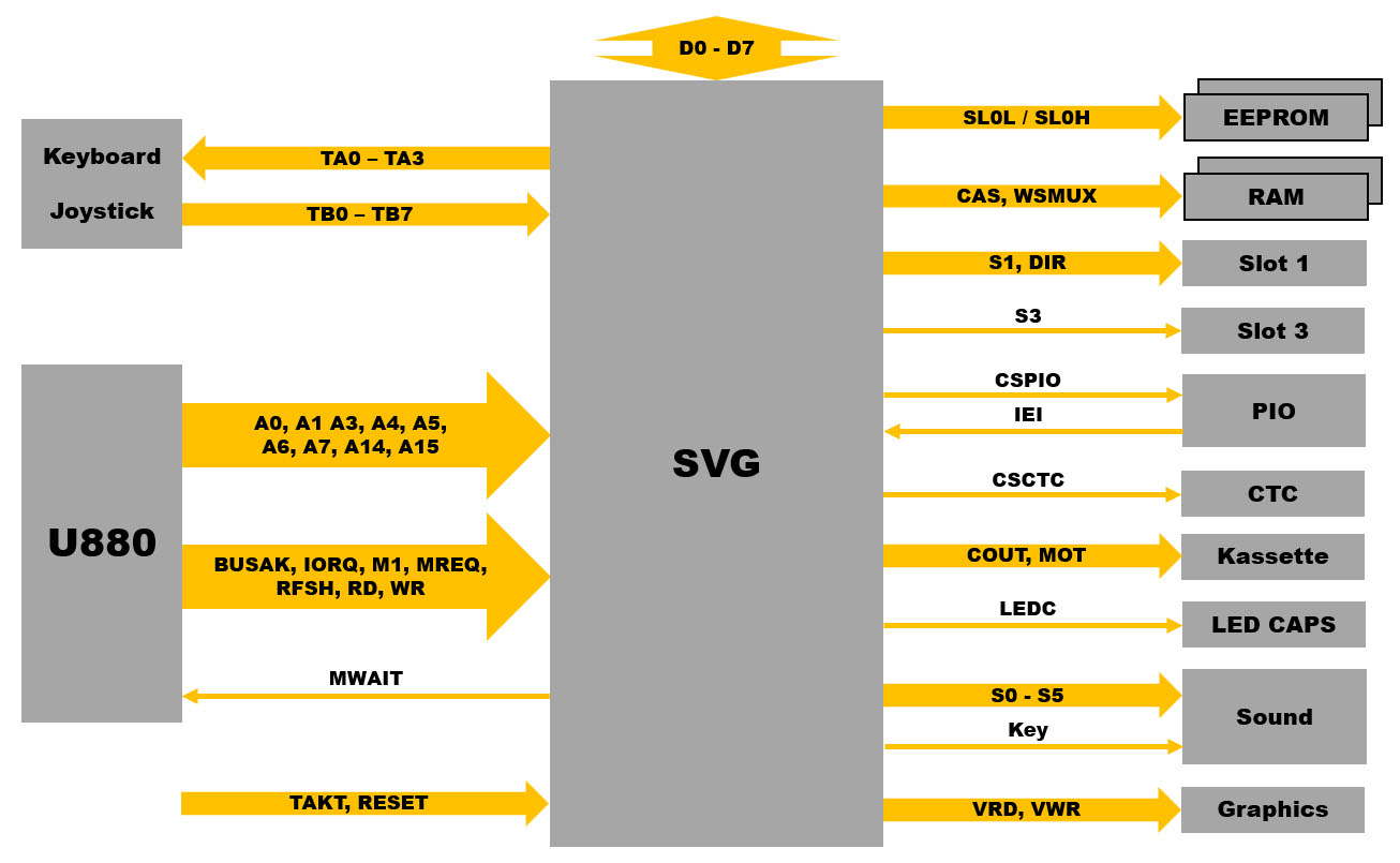
The interfaces of the U1525FC007 can be extracted from the circuit diagram of the Robotron A5105 educational computer. The module is connected to the 8Bit wide data bus and receives the clock signal and the reset signal, which is also used by the processor. The processor is a U880, which is functionally equivalent to a Z80. The U1525FC007 receives some control signals directly from the processor, from which it generates the MWAIT signal, among other signals. Nine address lines are processed from the 16-bit wide address bus. The module checks the keyboard or joysticks and generates the sound. The U1525FC007 also supports the U880 in the selection of various function groups: ROM, RAM, optional plug-in cards, PIO and CTC module, graphics unit and an optional cassette drive.
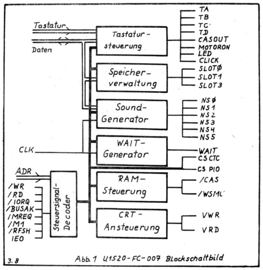
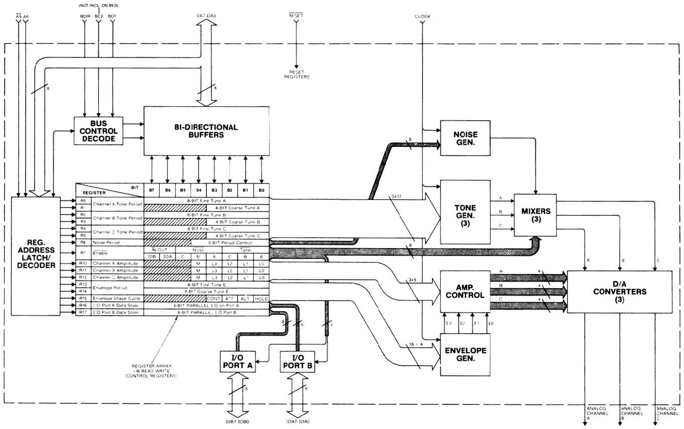
The papers presented at the 13th Microelectronic Components Symposium (Volume 7) contain some information on the U1525FC007. There the designation U1520-FC-007 is used, in which the chip size is missing. In addition to the abbreviation SVG, the component is also described as a "circuit for memory management and sound generation". The printed block diagram matches the integration in the Robotron A5105.
Like the Z80, the U880 can control a maximum memory volume of 64kB. The U1525FC007 extends the address table. The Robotron A5105 contains two EPROMs with a volume of 32kB and 8kB. There are also two DRAM modules, each with 32kB. The memory can be expanded using plug-in cards. The Microelectronic Components Symposium mentions 256kB of RAM. It is more plausible that the memory area can be expanded to a total of 256kB. The RAM may then be a maximum of 192kB in the A5105.
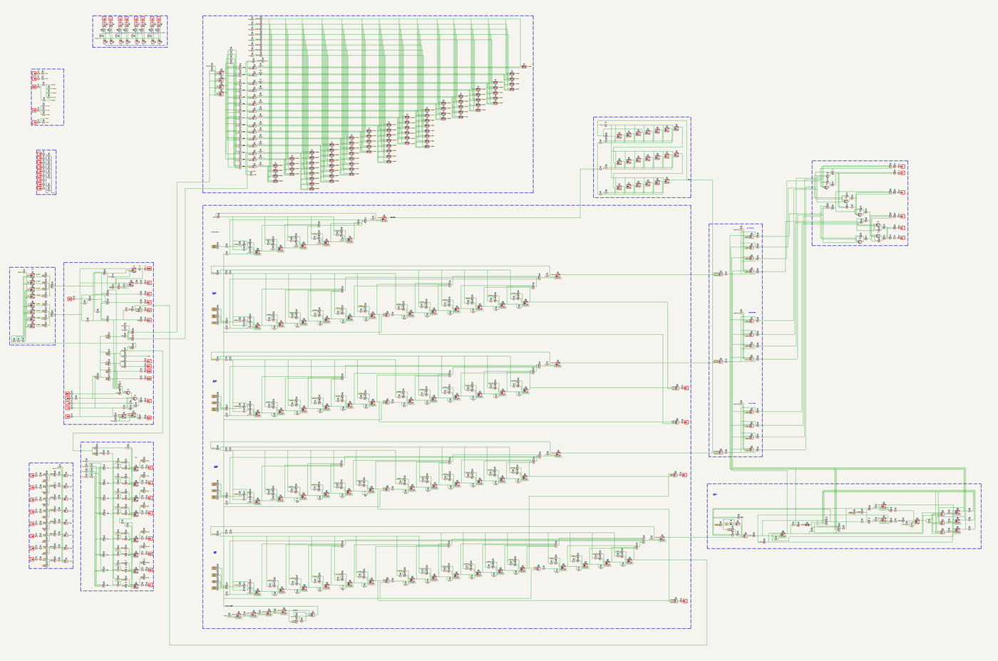
The logic in the U1525FC007 has been completely transferred to a KiCad circuit diagram. The use of only one sheet simplifies the creation of the logic circuit, as you can work more creatively. In addition, there are very large circuit blocks, the division of which would have an unfavourable effect on clarity. The thick blue frames represent a demarcation of self-contained function blocks. The block diagram from the 13th Microelectronic Components Symposium was not yet available here, which is why the layout of the circuit is not based on it. However, the block diagram is fully consistent with the extracted functions.
The KiCad file can be downloaded here:
https://www.richis-lab.de/images/35x64.kicad_sch (2MB). Such large graphics cannot be packed into common image formats such as JPEG. An SVG file is available here:
https://www.richis-lab.de/images/35x83.svg (14MB). It can be opened and edited in Inkscape.
The following relationships and functions have been extracted and documented as good as possible. However, it is quite possible that minor errors have crept in, individual addresses are not quite correct or potentials have been inverted.
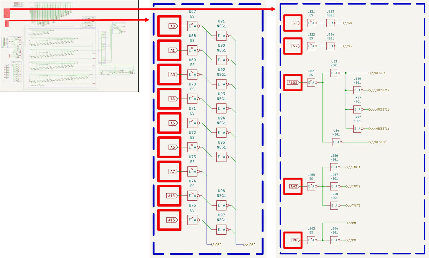
Some interfaces can be used as a starting point for the documentation of the circuit. These include the address bus, for example. The global identifiers outlined in red are the interfaces to the outside, i.e. the bondpads. Internally, most connections are shown as continuous lines. Only some highly branched potentials, such as the address bus, are distributed on the circuit diagram with so-called hierarchical identifiers. The address bus first passes through the input gates. Most address lines are also inverted for further use.
Further global signals are collected on the right, for example the read and write signals. The reset signal serves a total of 55 gates. The large number is probably one reason why five inverters pre-process the signal. The clock signal only serves seven gates, yet three inverters have been integrated here. The requirements for signal integrity were probably higher than for other signals. In the Robotron A5105, the PM potential is connected to the 5V potential via a pull-up resistor. The function of this potential will be considered in more detail later.
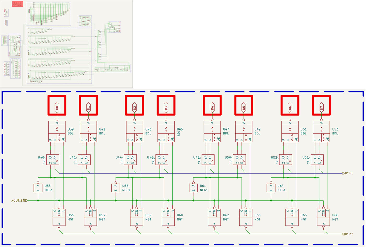
The data bus is routed to bidirectional interface gates with tristate function. These interface gates are controlled via TRIS gates. The /OUT_EN signal controls whether data may be placed on the data bus or whether the current potentials are to be read in. Clocked inverters are used to read in the data. An internal data bus is generated from this circuit.
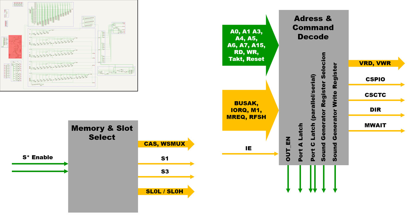
A function block controls the addressing of the memory areas. SL0L and SL0H each activate one of the two EPROM modules. S1 and S3 can be used to select the two interfaces for optional modules. The selection of the two 32kB RAM modules is controlled via CAS and WSMUX. Everything is controlled via the internal control signals S1 and S2.
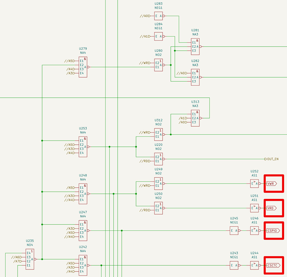
The second function block generates a whole series of control signals based on the address lines and the control signals of the U880. In addition, the interrupt output of the PIO module is analysed. The read and write signals for the graphics unit, which also serve as selection signals, are output directly. The selection signals for PIO and CTC are also output directly. The DIR signal defines the flow direction of the data transceiver at the connectors for the optional modules. The WAIT signal is used to signal to the processor when the addressed resource is available.
The right-hand function block also generates some internal control signals. One of these enables data to be transferred to the data bus. Further control signals can be used to transfer data to the internal registers. In the presentation from the Microelectronic Components Symposium, two of the registers are labelled Port A and Port C. Port A is written in parallel. Port C can be written in parallel or serially via two control signals. The integrated sound generator has very extensive configuration options. The register to be written to is selected via a control signal. A second control signal can then be used to write to this register.
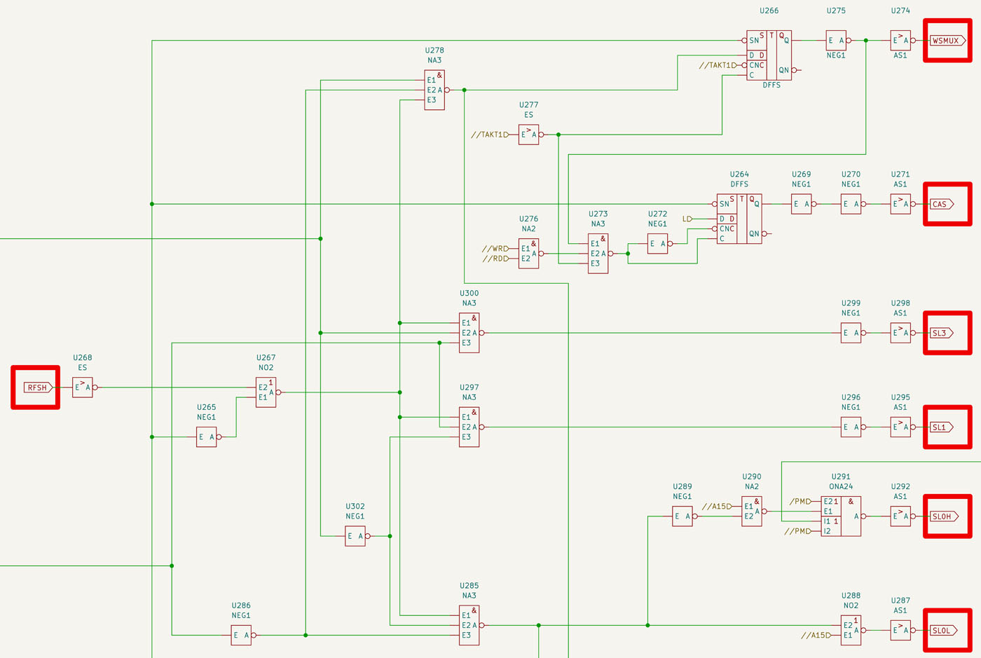
The control signals SL0L, SL0H, SL1, SL3, WSMUX and CAS are selected by linking the internal control signals S1 and S2 with the control signals of the processor. S0L and SL0H are also dependent on address bit A15.
WSMUX and CAS also have flip-flops which ensure that the address of the processor is split into row and column selection. If MRQ is active, the RAM immediately takes half of the address as row selection. If the RAM is selected, the circuit in the U1525FC007 ensures that the second half of the address is switched through to the RAM with WSMUX and this part is subsequently adopted as column address with CAS.
At first glance, it seems strange that the row selection in the RAM always takes place, even if the RAM is not selected at all. This transparency is necessary so that the DRAM can be refreshed, which the U880, like the Z80, carries out automatically. As the DRAM only outputs data on the bus with a column address, the selection of a row address alone does not lead to a bus collision.
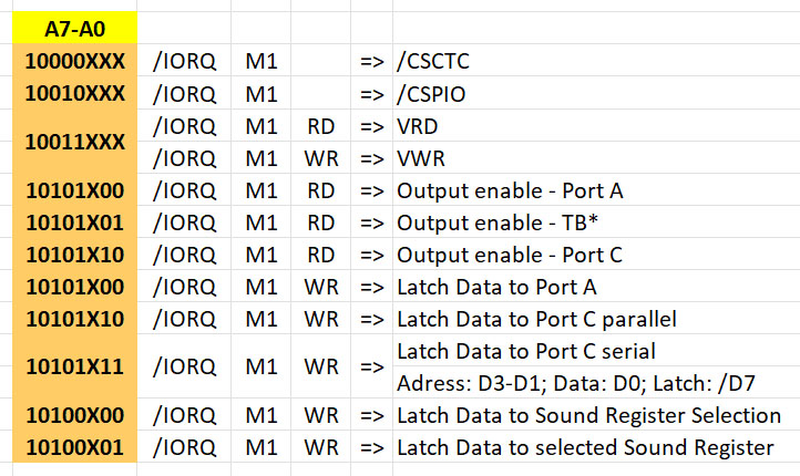
The decoding of the control signals is quite clear. The links between the addresses and the control signals can be easily extracted. While MRQ indicates an access to the memory area, the processor uses IORQ to communicate an access to a peripheral circuit. The signal M1 belongs to such an interrupt cycle.
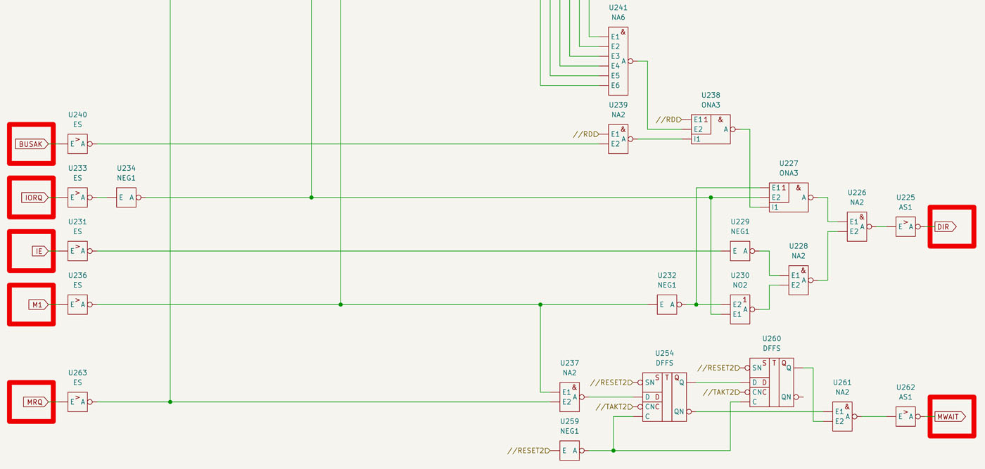
The generation of the DIR and MWAIT signals can be seen here. The U1525FC007 only inserts a fixed delay between the start of a memory interaction and the positive feedback via MWAIT.
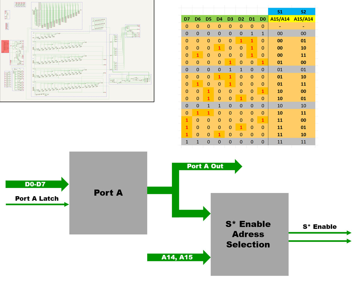
The Port A register can be used to configure the addressing of the memory areas. The current value of the data bus is saved in port A with the corresponding control signal. The stored value can also be read out.
Depending on which of the eight bits are set in port A, different combinations of address bits 14 and 15 are required to activate the control signals S1 and S2. Various combinations do not make sense. In all probability, only two bits are ever set in port A. Combinations that activate S1 and S2 with the same address combination also appear to make little sense and are painted grey here.
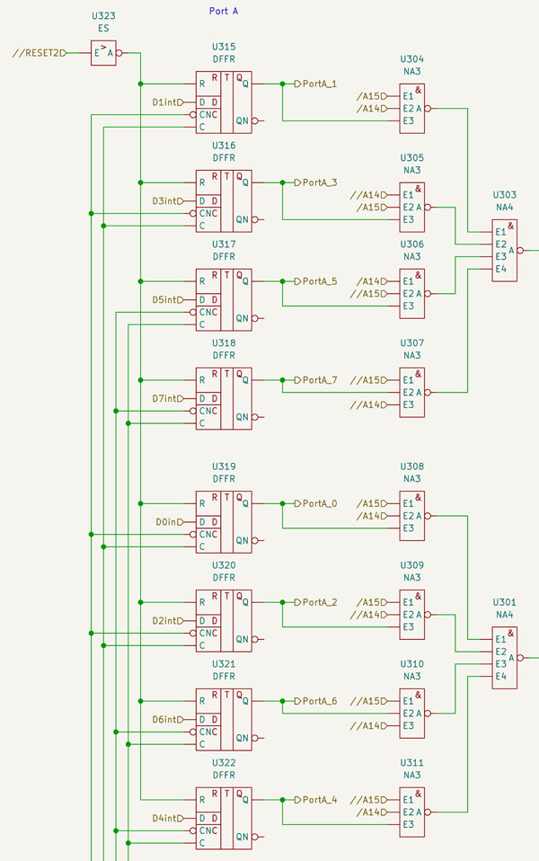
The Port A register is build with DFFR flip-flops.
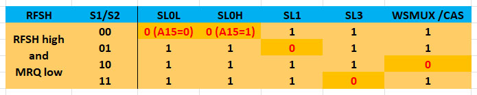
To be able to select a memory area, RFSH must have a high level and MRQ a low level. This means that there is no refresh cycle active and the processor wants to access a memory. The control signal combinations 01 and 11 can be used to select the interfaces of the optional plug-in cards (SL1/SL3). 10 activates WSMUX / CAS and thus the interface of the RAM modules.
SL0L and SL0H, the two EPROM modules, are only active if no bit is set in the Port A register. This appears illogical at first glance, as no other memory area can be activated in this state. Port A must first be rewritten. However, this implementation has the advantage that the EPROMs where the program is located can be accessed immediately after a reset without initialising the SVG. By linking to address bit 15, the control of the EPROM initially appears completely transparent to the processor.
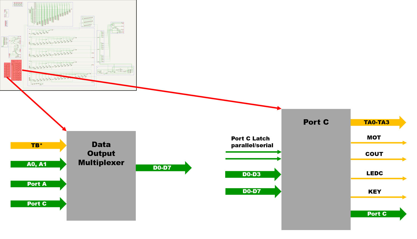
A multiplexer makes it possible to place various data on the data bus. One data source is the TB* inputs, which show the processor which key on the keyboard is pressed. Alternatively, the data in the Port A or Port C registers can be placed on the data bus. One of the three data sources is selected via the address lines A0 and A1.
The data register Port C can be loaded with data in parallel or serially. The content of the register controls the line selection of the keyboard logic (TA*), the cassette recorder, the caps lock LED and the signal for the key tone.
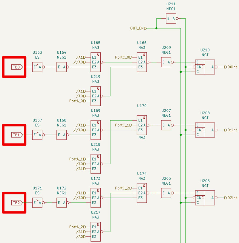
Here you can see a part of the multiplexer.
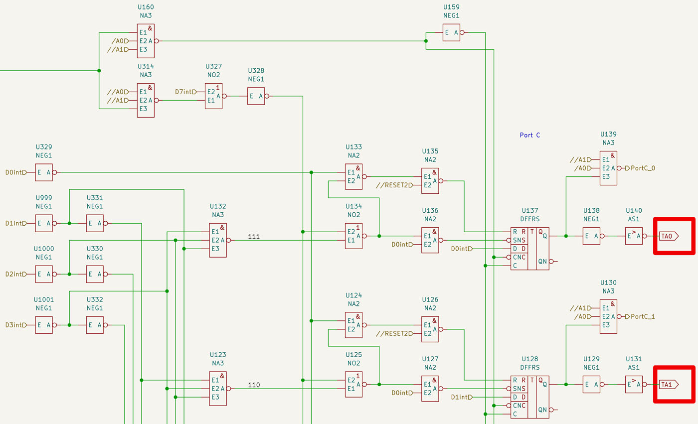
The Port C register is constructed with DFFRS flip-flops. The register can be loaded in parallel via the D inputs. Serial loading takes place via the set and reset inputs. The underlying logic evaluates the level of data bit 0. Data bits 1 to 3 define which bit of the register is to be written.
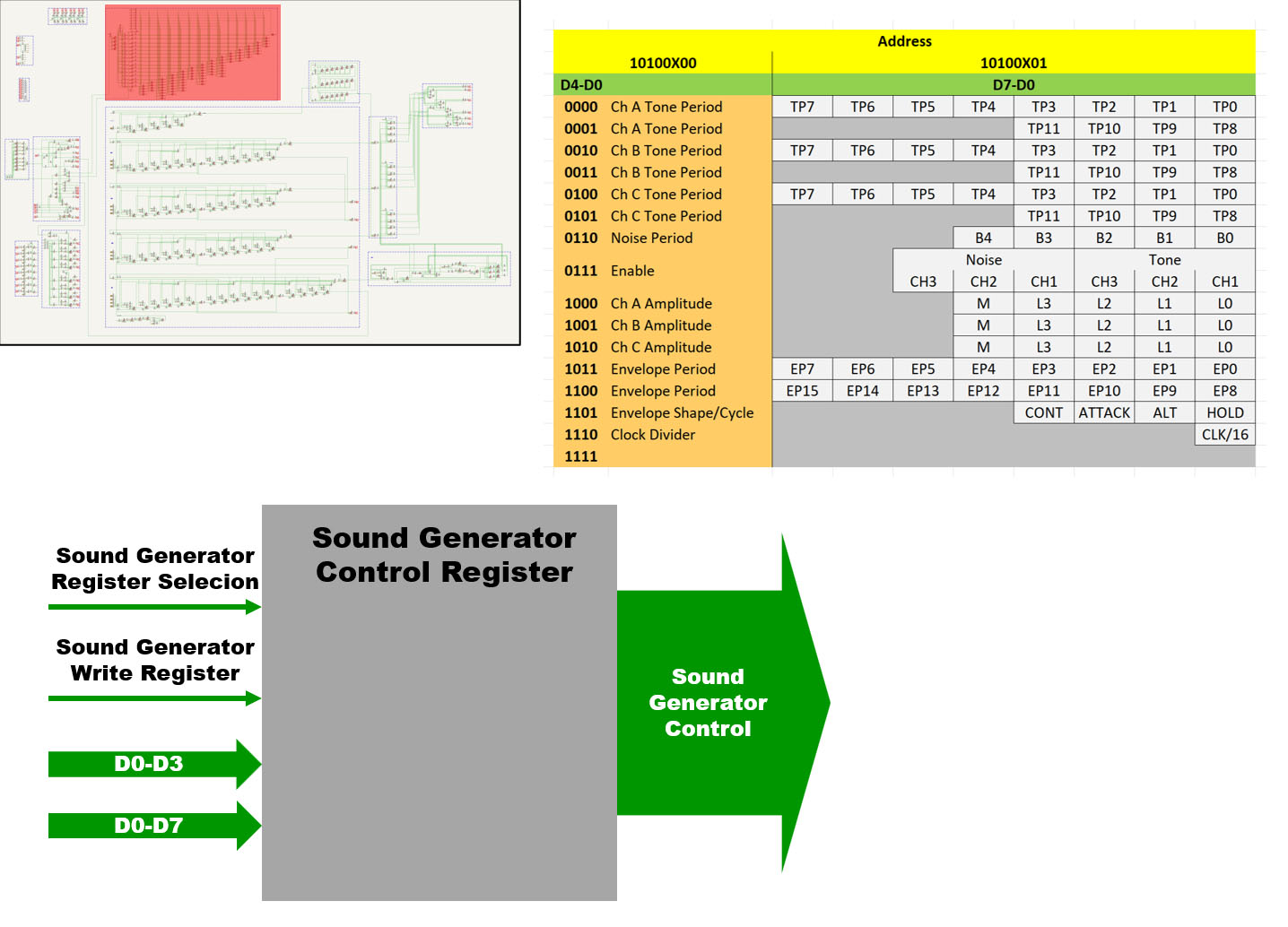
The sound generator takes up a lot of space in the U1525FC007. The configuration registers account for a large proportion of this. There are 16 registers with a total of 83 bits.
The sound generator integrated in the U1525FC007 is very similarly to the AY-3-8910 sound generator from General Instrument. Even the control registers have the same structure and arrangement. The U1525FC007 only lacks the Port A and Port B interfaces and the mixer at the output mixes the signals into a single channel. In addition, the digital-to-analogue converter is located externally.
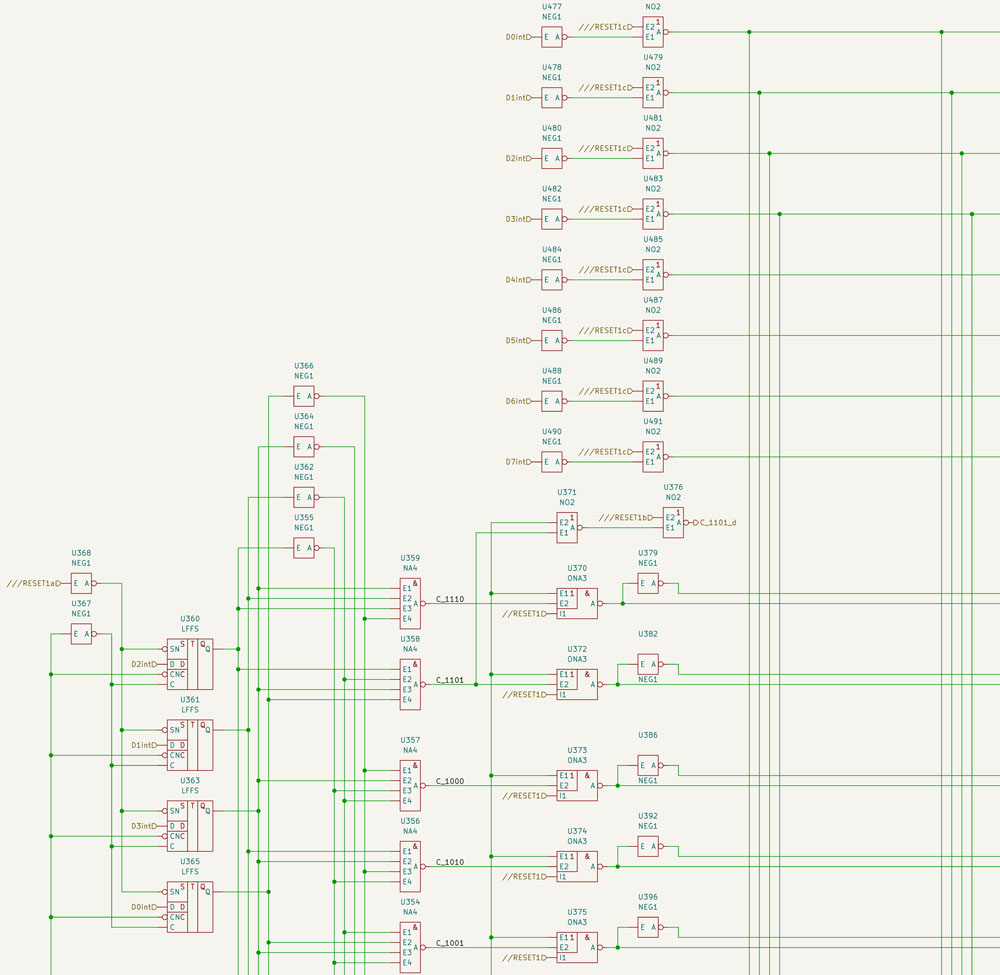
Four LFFS flip-flops use the first four bits of the data bus to select a line of the configuration register for the sound generator.
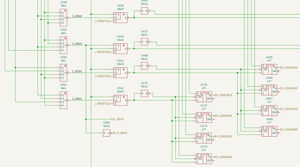
With some additional logic, the LFFS flip-flops generate the clock signals for LFF flip-flops, which represent the configuration registers themselves. The inputs are connected to the data bus. One address triggers the LFFS flip-flops and thus the line selection. Another address then allows the LFF flip-flops to accept the data on the data bus.
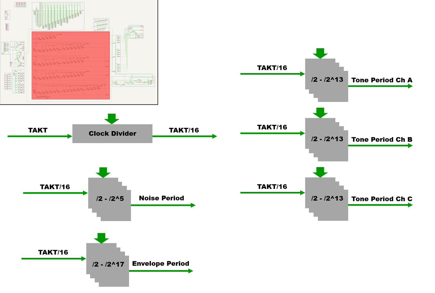
The sound generator is based on six clock dividers. The 3,75 MHz basic clock of the A5105 can first be divided down by a factor of 16 before it is then passed to the five other clock dividers as a working clock.
One clock divider defines the basic frequency of the noise generator and can divide the working clock by 2 to 2^5. A further clock divider generates the clock for the amplitude modulation with a divider factor of 2 to 2^17. The three tones that the sound generator can supply are generated via three clock dividers, each with a divider factor of 2 to 2^13. This results in a frequency range from 28Hz to 117kHz.
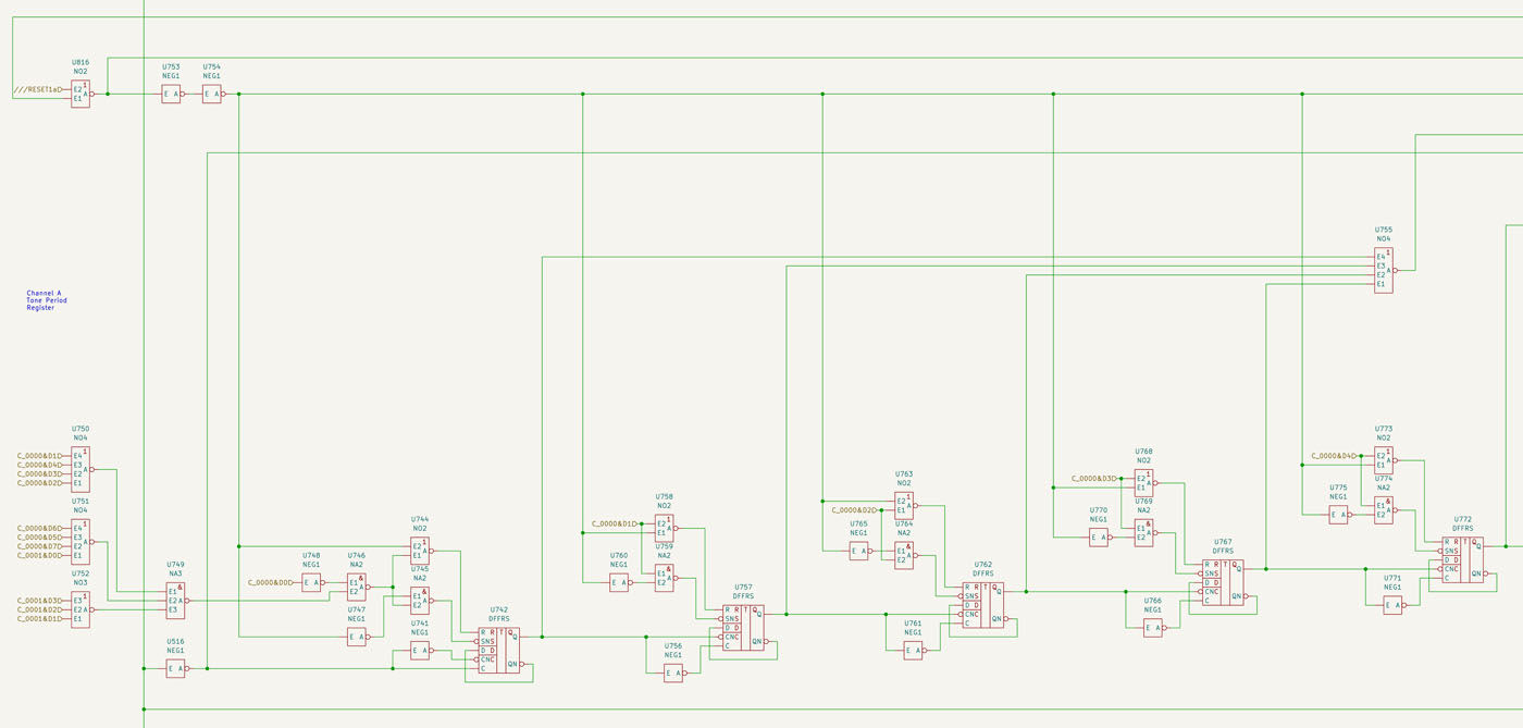
The clock dividers are based on DFFRS flip-flops. Their exact mode of operation only becomes apparent at second glance. The circuit not only takes up a lot of space on the circuit diagram, but also on the die.
The interfaces PM, OP0, OP1, OP2 and OP3 appear to be used for diagnostic purposes. The frequency dividers of channels A, B, C and the envelope generator are divided into groups of six and one group of four. This results in nine groups that can be read out individually. The selection signal for register 0010 switches the four OP outputs, making it possible to reach eight of the nine groups. The PM input can be used to isolate the groups from each other and feed them with the same clock signal. The PM signal also switches the remaining group to the S0H output.
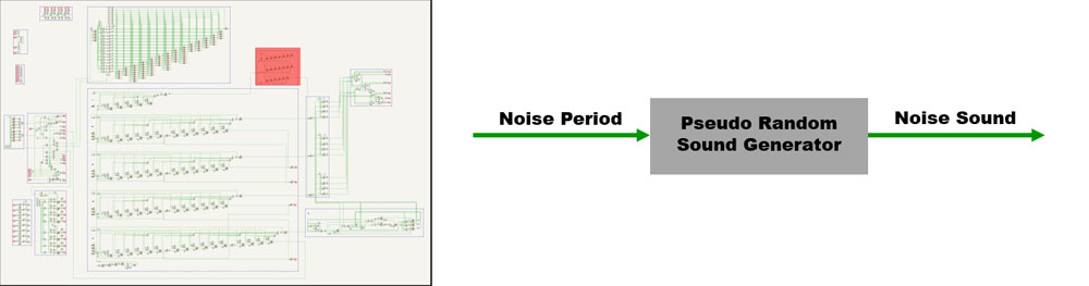
The sound generator contains a noise generator that also uses a divided clock frequency.
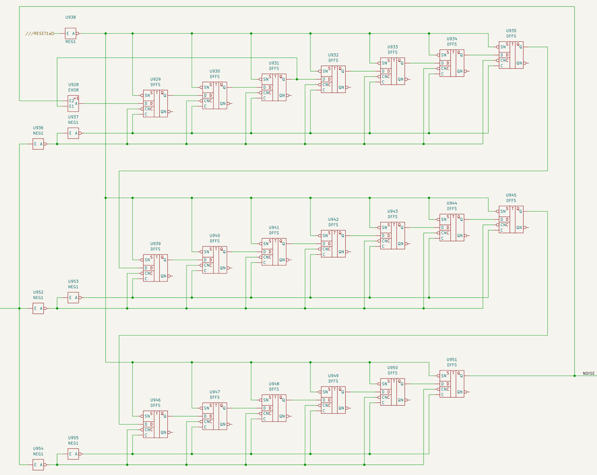
Of course, this is only a pseudo-noise generator that does not really generate random noise. There are 20 DFFS flip-flops connected in series. The input signal is generated by an EXOR gate, which links the current output signal with the output signal of the third flip-flop. This results in a pseudo-random output signal.
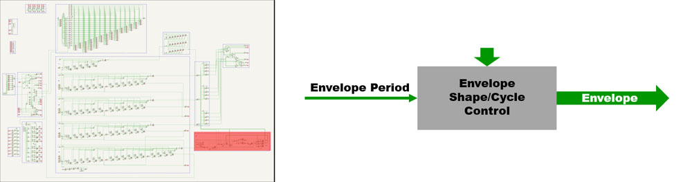
The envelope, i.e. the amplitude modulation of the output signal, can be defined with a further circuit section. The basis here is also the divided working clock.
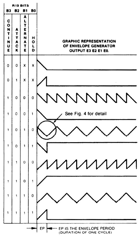
The datasheet of the AY-3-8910 shows which envelopes can be generated. The circuit itself is rather confusing. It feeds four data lines, the value of which represents the current amplitude.
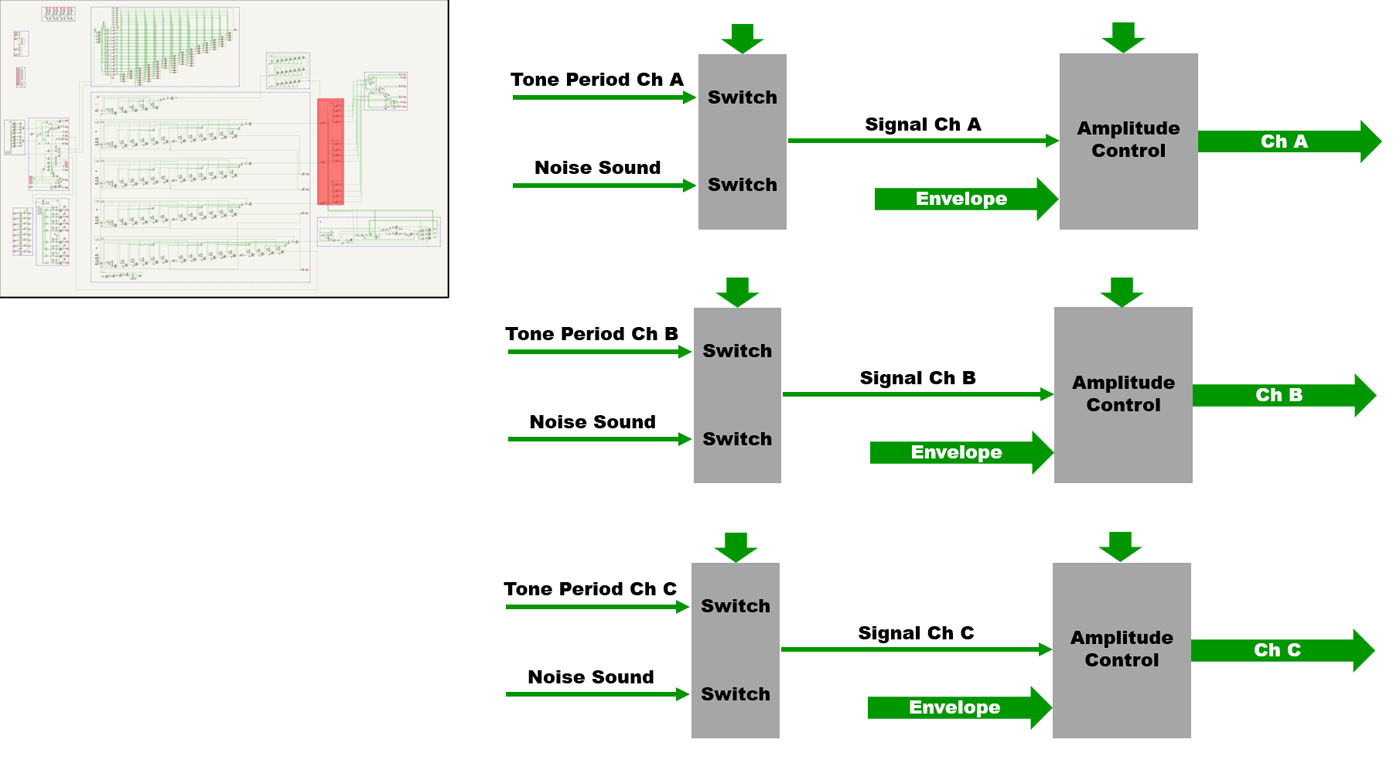
The configuration register ultimately defines which of the three tones is forwarded. Each tone can be linked to the noise signal or just the noise signal can be forwarded. The three signals then pass through an amplitude control, which can be set via the configuration register and is also modulated with the generated envelope function.
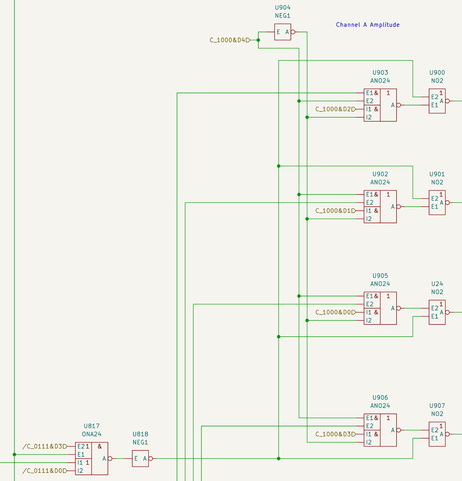
Here you can see the circuit for one channel. The tone or the noise signal or both signals are selected in gate U817. The NOR gates on the far right pass on the signal if the ANO24 gates in front of them allow this. The amplitude configuration and the envelope information are linked in these gates. The four outputs all carry the same signals when they are active. Depending on which of the outputs are active, different amplitudes will result later.
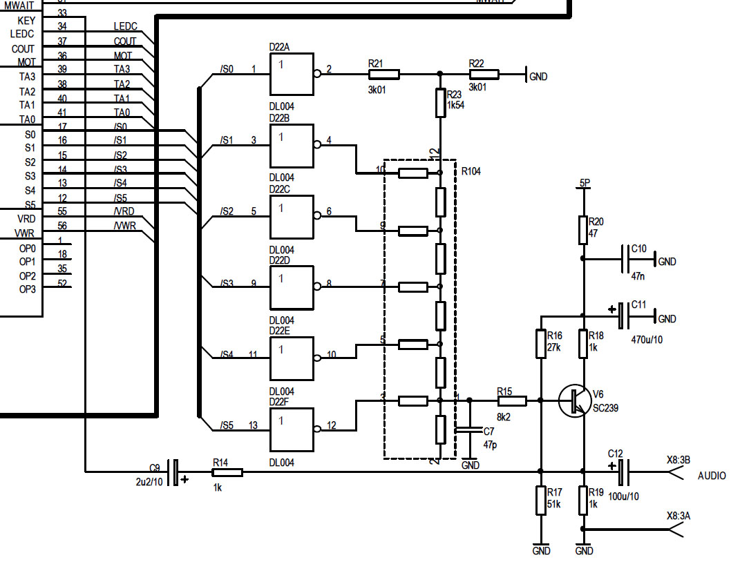
The functionality of the sound output becomes clearer if you take a look at the circuit diagram of the A5105. There, a resistor chain represents a discrete DAC. Each S output serves an inverter, which influences the output level more or less depending on the connection point.
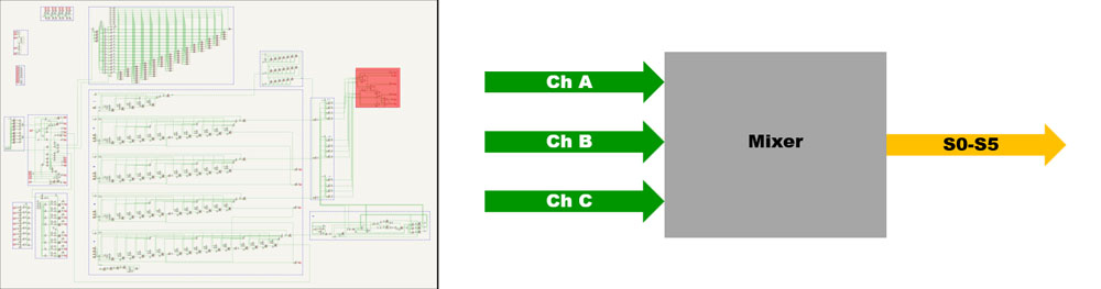
Before the sound signal is delivered, a mixer combines the three generated channels.
https://www.richis-lab.de/logic30.htm 


