I wasn´t happy with my explanation how these two matrices in the CA3161 do they job.
Now I know what the problem was! That is a I2L, a integrated injection logic!
The binary value, here 1110, is located with its complementary value at the lower edge of the matrix. A low level at an input pin leads to an active low level at the lower edge of the matrix (2^3). A high level leaves the respective input open (2^0 - 2^2). The complementary connections behave correspondingly inverse to this.
The matrix contains a so-called Integrated Injection Logic, I2L. If there is a low level at one of the vertical stripes, the outputs remain inactive. Without a low level, the Integrated Injection Logic switches a low level to the outputs.
A total of 15 lines lead to the left. 15 lines are sufficient because no active control is needed for the number 8. The selected line remains inactive. All other lines carry a low potential.
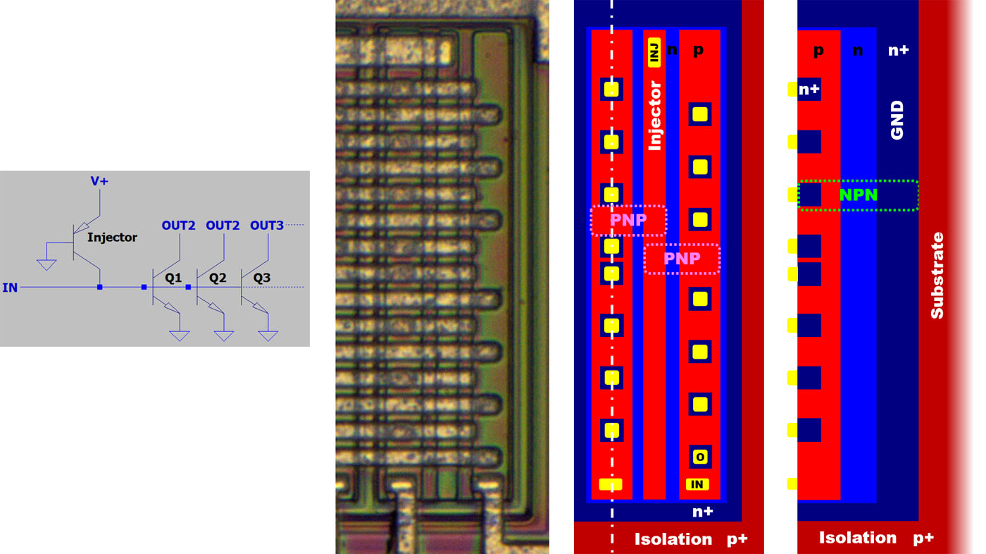
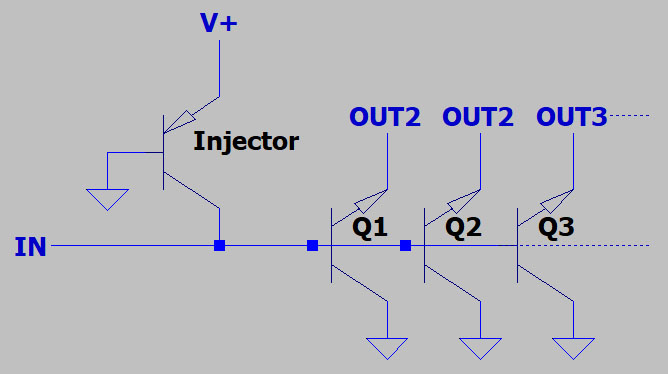
At the input of an Integration Injection Logic there is the injector, a PNP transistor whose base is connected to the ground potential and thus serves as a current source. In this circuit, the injector is not directly connected to the positive supply, but to a current source. This probably reduces the power dissipation. Any number of lowside transistors can be connected to the input as a signal source. The outputs of an I2L gate are then again NPN transistors which switch to GND. Again, theoretically any number of outputs are possible.
On the die of the CA3161 the NPN transistors of an I2L gate can be seen as long vertical base strips, in which square emitter areas are located. An injector strip is integrated between two of these strips. The injector does not necessarily have to be designed as a long strip parallel to the NPN transistors. A single block at the upper end would be sufficient in principle. However, the long strip reduces the switching delay between the top and bottom NPN transistors. This feature can be critical, especially with long I2L gates, such as those present here.
The PNP transistor, operating as an injector, forms between the middle and adjacent p-doped strips. The n-doping, in which the strips are embedded, represents the base, which is connected to the ground potential via a buried heavy n-doping.
At first glance the structure of the NPN transistors corresponds to the usual design. In an n-doped well with a low-lying, heavily n-doped feed line, there is a p-doped area containing heavily n-doped elements. Normally, the lower n-doping represents the collector and the upper n-doping forms the emitter of the NPN transistor. However, here the transistor structure is used inverted. The lower well is operated like an emitter and the individual squares in the base doping operate as collectors. Therefore, the above schematic describes the physical structure more accurate.
The common transistor structure is advantageous because a thin base layer can be set there. Most of the electrons, which are released from the emitter, fly through the base zone and reach the collector. The doping gradient that occurs in the base region also has a beneficial effect on this movement. In an inversely operated transistor, the electrons that then leave the large-area collector have many more opportunities to leave through the base. Only a few electrons reach the small emitter.
NPN transistors certainly allow inverted operation. The breakdown voltage and and gain are then usually much lower. The same applies to the cutoff frequency. On the other hand the lower saturation voltage is advantageous. The negative effects can be advantageously influenced to a certain extent by the shape and doping of the structures. A more detailed consideration can be found, for example, in the IEEE article "Device Physics of Integrated Injection Logic" (IEEE Transactions on Electron Devices Volume 222, Issue 3, March 1975).
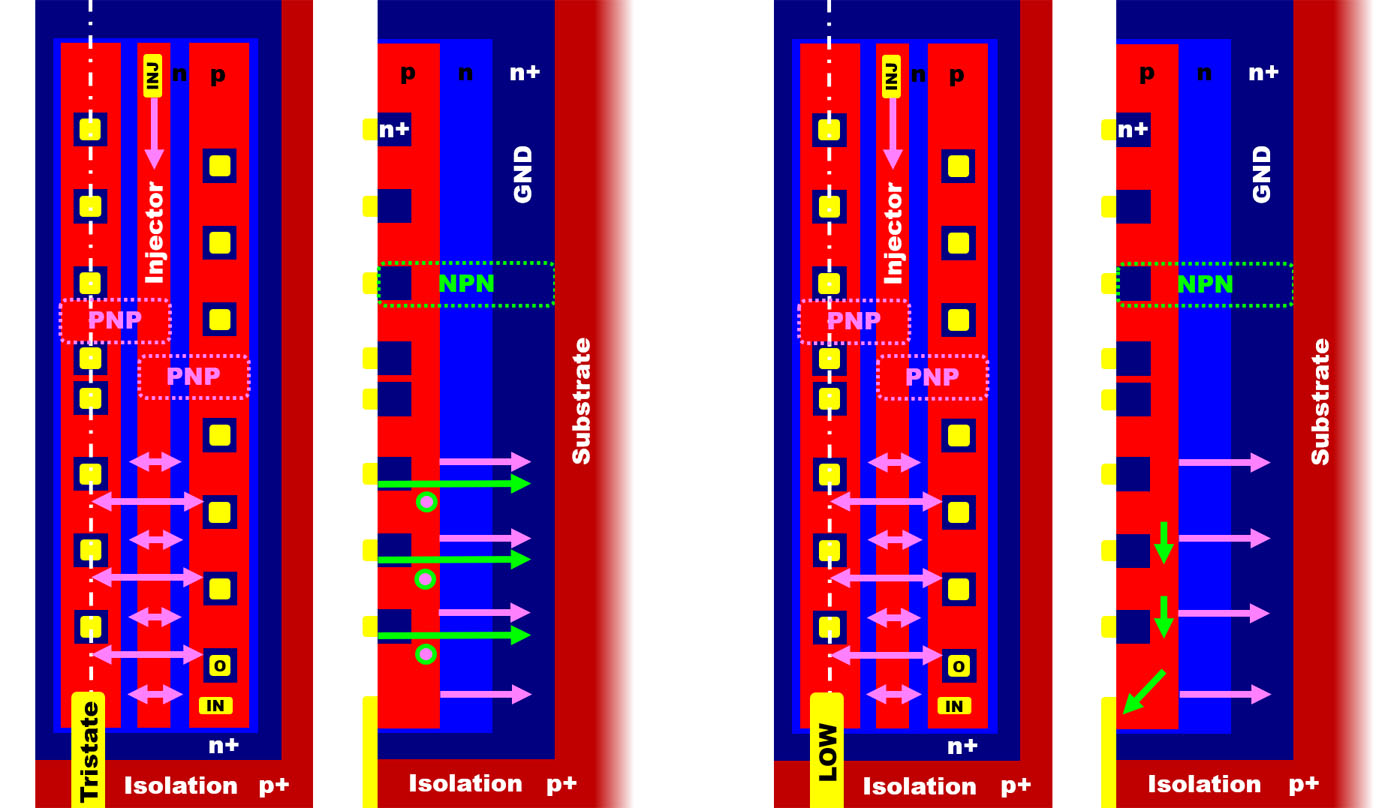
If no signal is present at the input of the I2L strip, the current flow through the injection transistor (pink) ensures that the NPN transistors become conductive and pull the outputs to ground potential (green).
If there is a low level at the input of the I2L strip, the free charge carriers of the injection transistor are diverted from the base area of the NPN transistor so that it remains blocked.
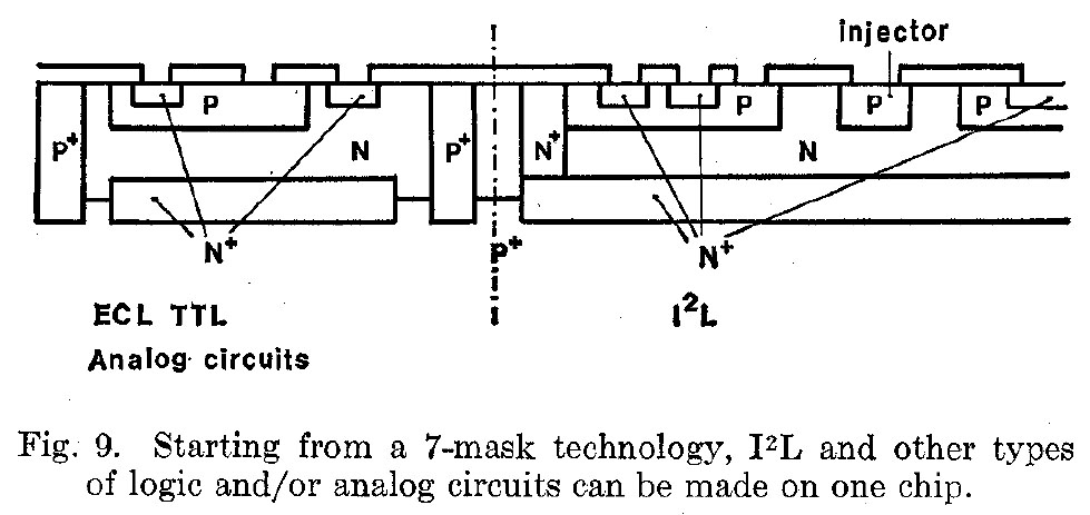
Integrated Injection Logic can be integrated into an n-doped substrate. However in the CA3161 there are also ordinary transistors, which usually require a p-doped substrate.
The paper "Integrated Injection Logic-Present and Future," published in the IEEE Journal of Solid-State Circuits (Volume 9, Issue 5, October 1974), shows how seven masks can be used to integrate I2L areas alongside conventional transistors. As usual for normal transistors a heavily p-doped substrate is used to isolate the individual transistors from each other. Above this is the NPN transistor with a buried, highly doped collector feed line. Heavily p-doped confinement structures provide lateral isolation.
The I2L region is isolated by a heavily n-doped well. The collector feed line can be used as the bottom element. In addition just some strongly n-doped, deep-reaching lateral boundary structures are required. This also explains the different appearance of the boundery structures of normal transistors and I2L regions on the die of the CA3161.
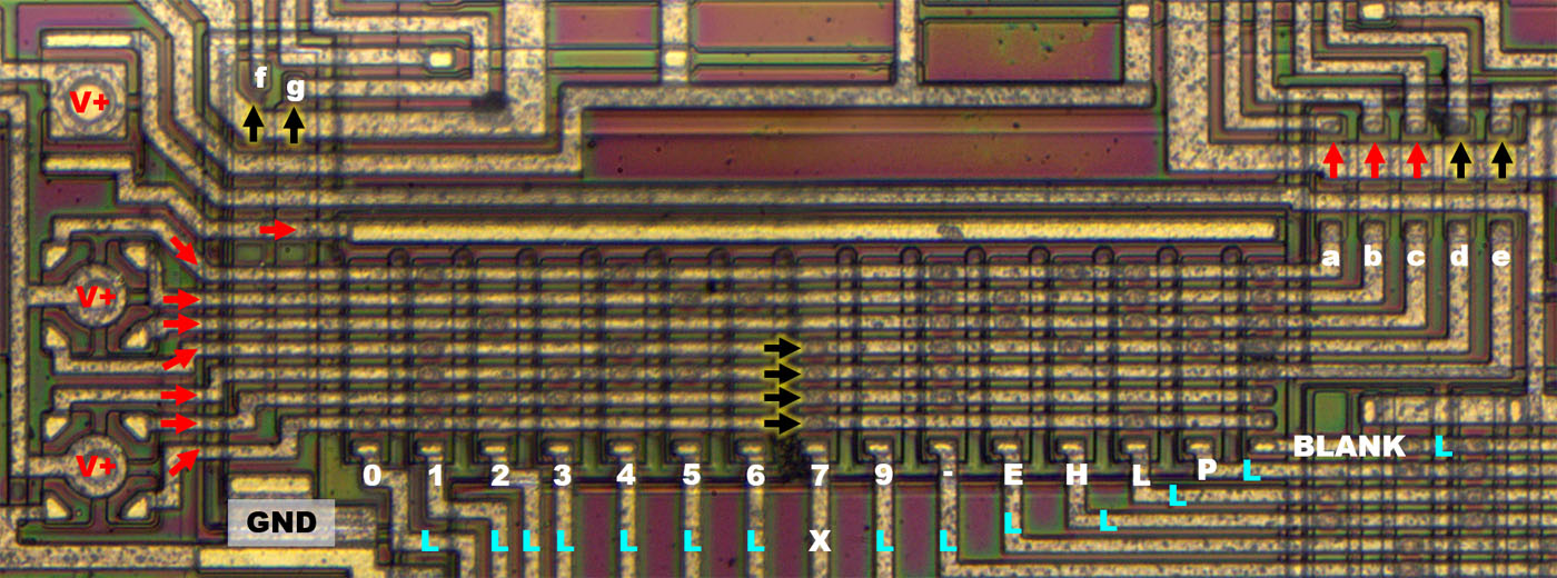
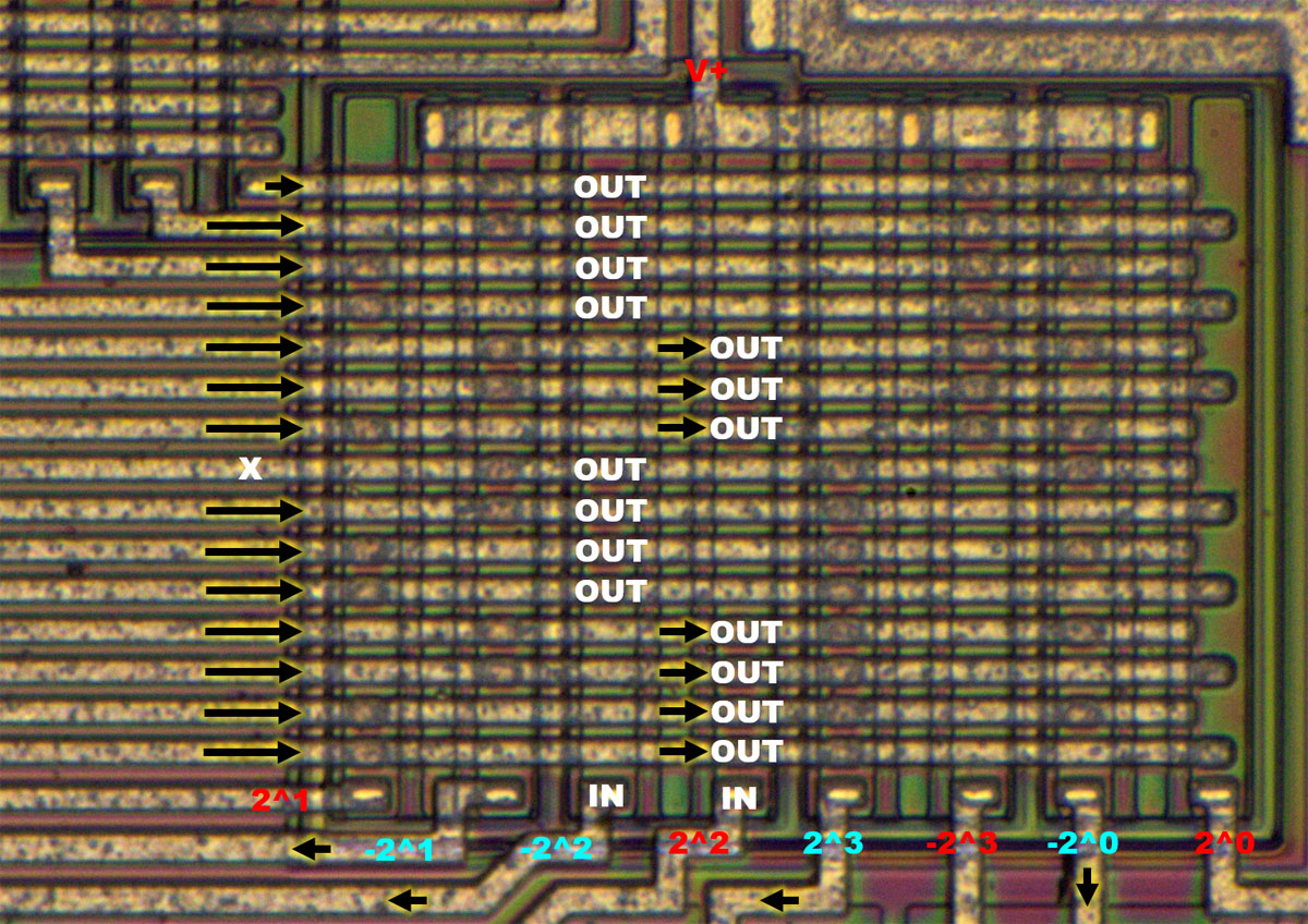
This first I2L matrix is followed by another I2L matrix, which ultimately controls the final stages of the device. Seven lines run horizontally, which stand for the seven segments. They are connected to current sources on the left, which provide a high level in the inactive state. The output stages that receive a high level are activated and the corresponding segments light up. Consequently, the matrix must deactivate the segments that are not needed. For this reason the number 8 is not present here, because without active intervention all segments are active and accordingly an 8 is displayed. Five lines lead to the right to the output stages a, b, c and d. The lines for the segments f and g run to the left of the matrix.
As with the first matrix, this is a Integrated Injection Logic too. At the top left is a dual power source. One path supplies the injector of the lower matrix, the second path supplies the injector of the matrix you can see here. Since the lines are not too high, it was sufficient to design the injector as a single element above the transistor strips.
Where no low level is present (X), the I2L transistors become active and deactivate the segments connected there (here d, e, f and g).
https://www.richis-lab.de/logic22.htm 


