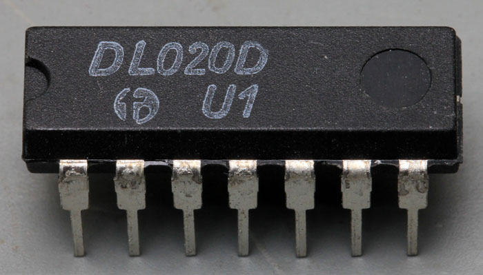
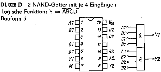
DL020D, a Dual-4-Input-NAND built by the Halbleiterwerk Frankfurt Oder. It´s a 74LS20.
We already had the D220 (
https://www.richis-lab.de/wafer01.htm) which is a 7420.
U1 => built in January 1986.
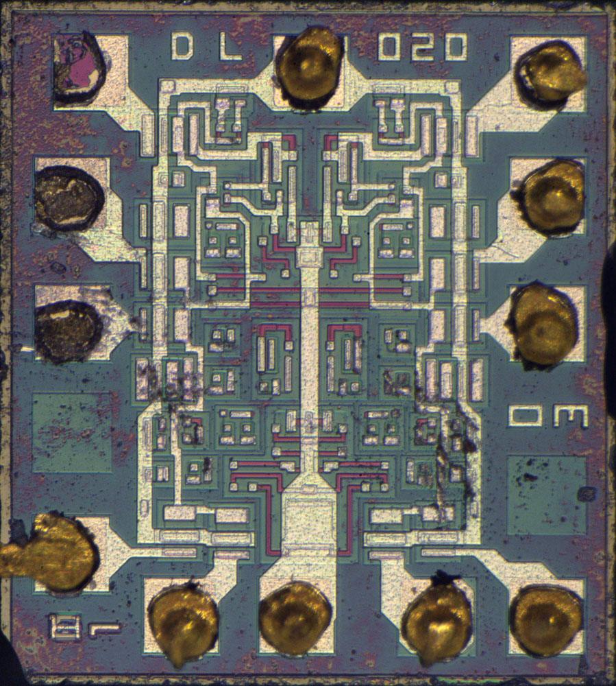
The die is 1,1mm x 1,0mm. The symmetrical design is easy to see and there are a lot of unused parts. I´m sure the design was used for different logic gates by just changing the metal layer.
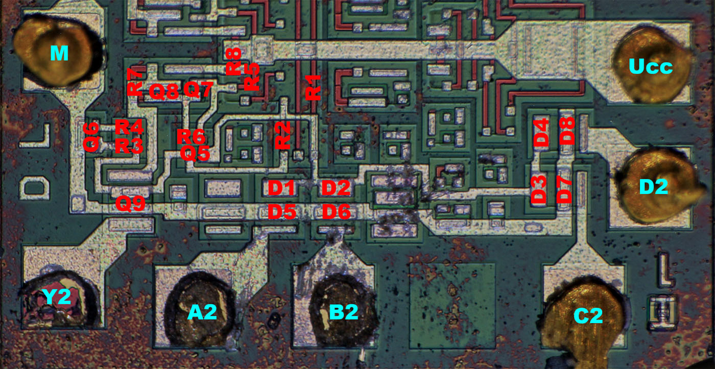
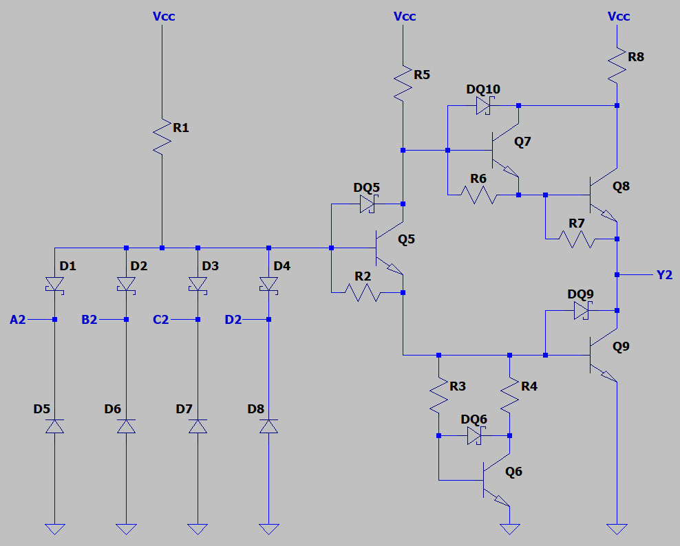
With the background knowledge how a 74LS logic is usually built, we can reconstruct the circuit of the DL020 fairly easily. The diodes D1-D4 isolate the inputs against each other. Since the diodes are in the signal path Schottky diodes are used, which offer fast switching times. The diodes D5-D8 seem to be normal diodes. They protect the DL020 against negative voltages.
If there is no low level at any input resistor, R1 pulls the base of Q5 high. Q5 is a Schottky transistor. A Schottky diode between base and collector ensures that the transistor doesn´t saturate so switch-off is faster. Despite the Schottky diode there is a resistor between base and emitter too. Through this resistor free charge carriers can flow out of the active area.
Around Q5 the potentials are tapped which control the highside and the lowside transistor in the output stage. The highside transistor is a Darlington (Q7/Q8). Q7 is a Schottky transistor which guarantees a fast turn-off. In the place of Q8 a normal transistor is sufficient. Base-emitter resistors are added too (R6/R7). The resistor R8 is necessary, because during switching the lowside and the highside transistor become conductive at the same time for a very short time. During this period the current should be limited.
Q9 is the lowside transistor. Again, this is a Schottky transistor. The network R3/R4/Q6 can be found in a lot of 74LS-logic of other manufacturers. I´m not 100% sure why you need this circuit. I assume the Vbe of Q6 ensures a faster turn-on of Q9. Other suggestions?
The pictures quality could be better but we can identify some parts and structures.
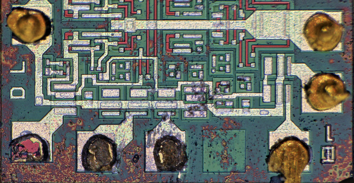
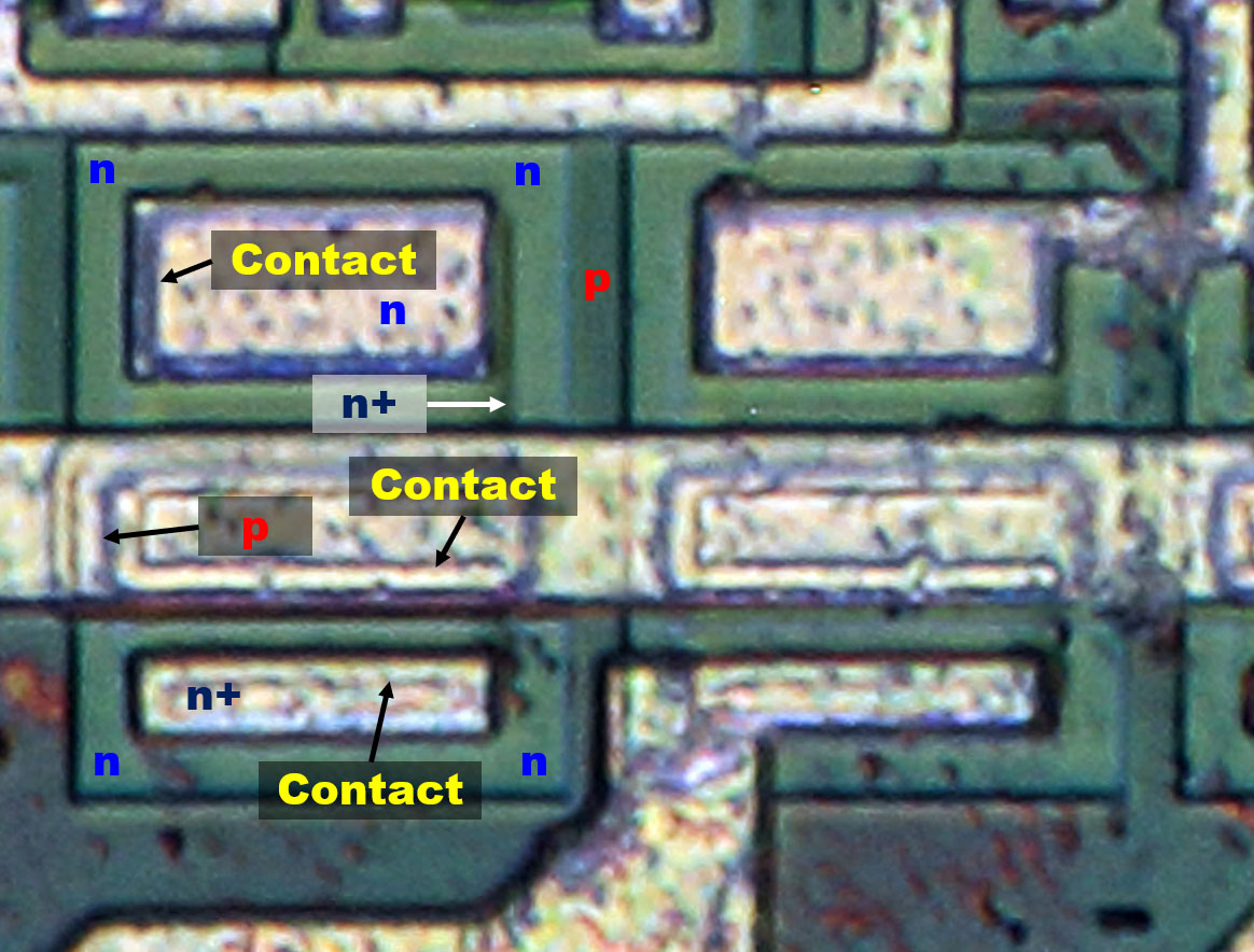
Here you can see two of the input structures, unused on the left side, used on the right side. The input signal is fed from the bottom edge. The horizontal line is connected to GND. The contacts at the upper edge are connected together.
One might expect that this is a transistor but there is no base area visible where two of the three contacts would have to be located. Instead the upper and lower contacts seem to be connected to the n-doped surface. The lower contact is slimmer than the upper one. With the background knowledge that there are usually Schottky diodes at the inputs of a 74LS-logic, these structures are quite argumentative. The lower contact is probably located on a heavily n-doped area which ensures an ohmic contact to the n-doping. Due to the high doping a small contact area is sufficient. The outlines which are barely visible are probably the vias in the insulating silicon oxide. The edges of the heavily n-doped area cannot be seen at the contact. A deeper, strongly n-doped layer conducts charges to the uppermost contact, where the metal layer rests directly on the "normal", weaker n-doped layer. Thus a Schottky diode is formed at the interface. The larger contact area is probably necessary due to the lower conductivity of the weaker n-doped material.
The contact in the middle of the structure is interesting. In most 74LS schematics, there are two Schottky diodes at each input. Here the protection diode seems to be a conventional diode. This can be assumed because another outline can be seen around the outline of the via. A strong n-doping would not serve any useful purpose at this point, it would even act as a low ohmic pull-down resistor. A p-doping on the other hand creates a conventional diode. The conventional diode is slower than a Schottky diode but it probably has advantageous properties in its function as a protection diode. Perhaps it can conduct higher currents in this process.
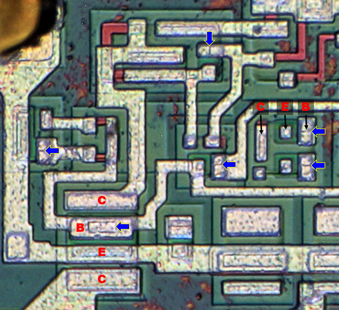
The Schottky transistors can be recognized too. Usually, the structure of a Schottky transistor hardly differs from the structure of a normal transistor. It is sufficient to enlarge the base contact area so it contacts the collector area too. At the contact between the base metal and the collector area the desired Schottky diode is formed. These double contact can be seen even in the smaller transistors of the DL020D. The base contacts are quite large and have an edge where the base and collector regions meet under the metal layer (blue arrows).
In the case of the large lowside transistor in the bottom left corner of the image, a relatively large square can be seen in the area of the base contact. The square is an opening in the base area through which the metal layer can contact the collector area.
https://www.richis-lab.de/logic09.htm 


