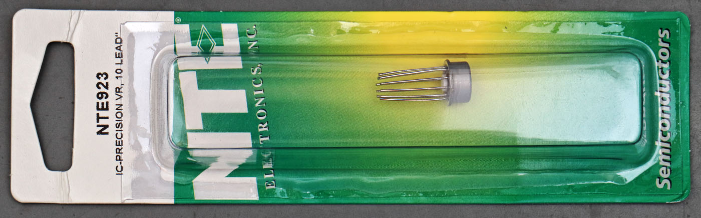
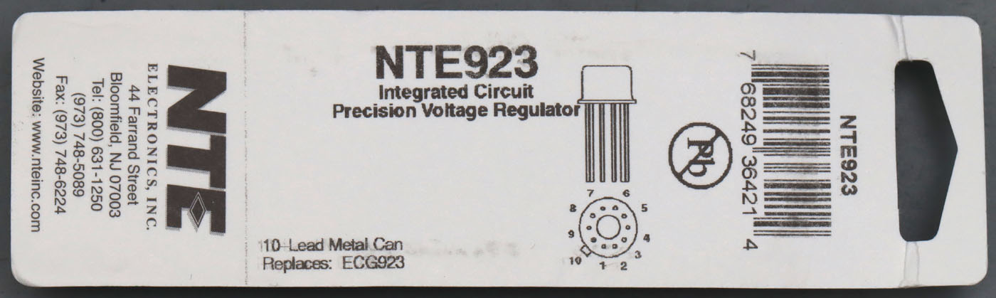
NTE still serves the aftermarket with 723 voltage regulators. These are sold under the name NTE923. On the back of the package it says that the NTE923 is the successor of the ECG923. The company ECG was taken over by NTE.
Nothing special on/in the package.
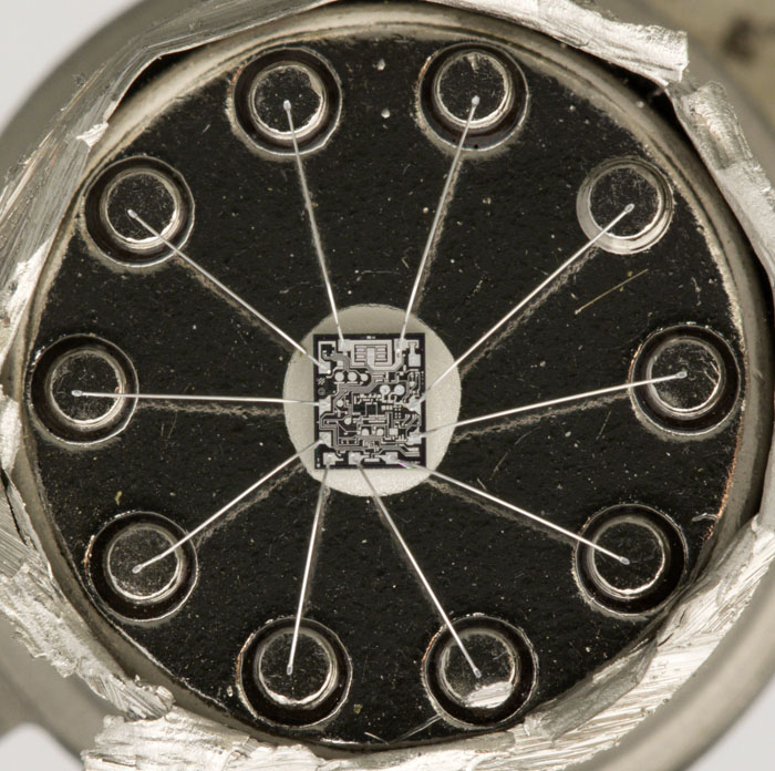
Here we see that NTE uses the bandgap version of the LM723 from National Semiconductor.
(LM723CH:
https://www.richis-lab.de/LM723_07.htm // LM723J:
https://www.richis-lab.de/LM723_02.htm)
The auxiliary structures are completely the same. Most likely NTE (or ECG) bought up the last batches from National Semiconductor. These could have been finished devices or uncut wafers.
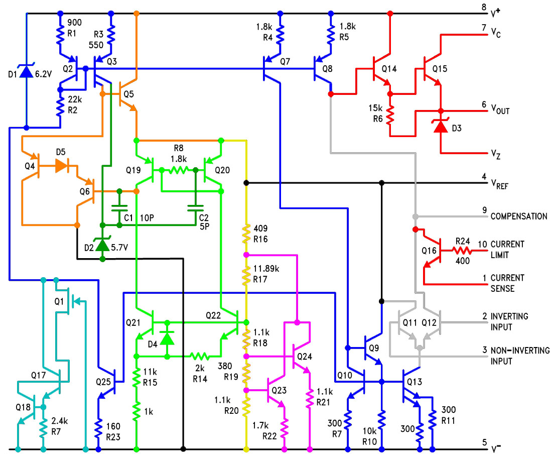
Now let´s take a look at the schematic. In my view the bandgap LM723 does its job like this:
The power section (red) is easy to recognize. Q14 is the driver transistor for the power transistor Q15. D3 is the Z-diode, which in some package is not connected to a pin. Q16 can sink the base current of the driver transistor and thus makes it possible to implement current limiting.
Also easy to recognize is the differential amplifier (gray), which is usually used to compare the actual value of the controlled system with a setpoint. The two input transistors Q11 and Q12 work with the current sink Q13 for this purpose. Q12 sinks the base current of the driver transistor if required.
The current sources and sinks of the device (blue) are current mirrors that use transistor Q2 as a reference. This transistor generates a relatively constant current using the Z-diode D1.
The self-supply is interesting. Via Q7/Q9/Q10/Q25 the transistor Q2 itself sets the current through the Z-diode that is necessary for its operation. To ensure that the circuit starts up safely, there is a small current sink (cyan) in the lower left area.
The reference voltage of the bandgap LM723 is generated with a Brokaw bandgap reference. The core of this reference is formed with the transistors Q21/Q22 with their resistors R14/R15 and the current mirror Q19/Q20 (light green). The current mirror ensures that an equal current flows into both branches. As described with the TL7705 (
https://www.richis-lab.de/TL7705.htm), a very temperature-stable voltage is established at the base of Q21 and Q22 if the current densities in the transistors and the resistor values are suitably designed.
The purpose of the diode D4 remains unclear.

It should not become conductive during normal operation. A protection of the base-emitter path against negative voltages does not seem to be necessary due to the high resistance values.
If the desired operating point in the bandgap reference has not yet been reached, the path Q6/D5/Q4 becomes conductive and reduces the current flow through Q5 (orange). Less current flows into the current mirror and into the voltage divider (yellow) of the bandgap reference. As a result, the operating point shifts until the same current flows through the transistors Q21/Q22.
The yellow voltage divider not only controls the transistors Q21/Q22, it also ensures that the desired reference voltage of typically 7,15V is set at the top resistor. The purpose of the transistors Q23/Q24 (purple) remains unclear. It seems that the circuit adds an additional temperature drift. For a Brokaw bandgap reference such an auxiliary circuit should not be necessary.
Capacitors C1 and C2 (dark green) stabilize the bandgap reference. It is interesting to note that the Z-diode D2 in combination with the current source Q3 generates an auxiliary reference for the capacitors. As will be shown this is necessary because the capacitors are not very voltage resistant.
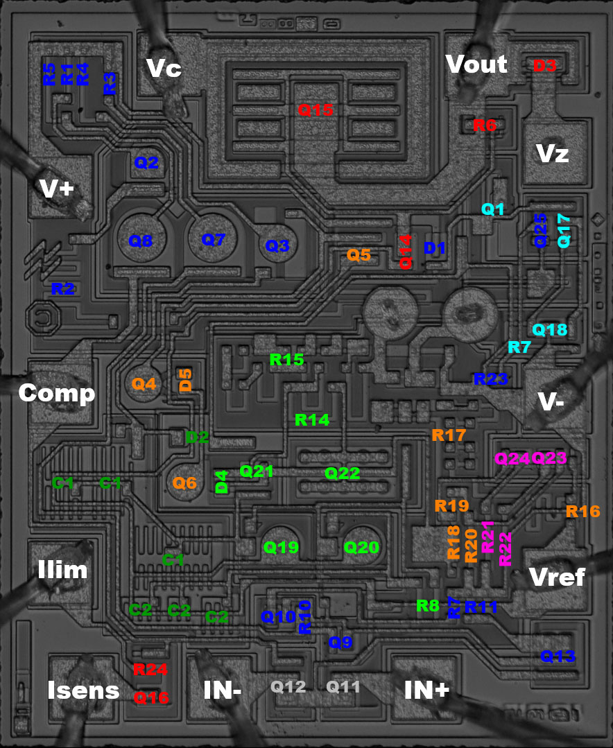
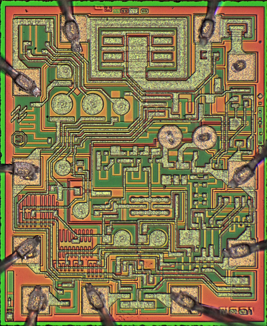
The individual elements can be found on the die as shown in the circuit diagram.
The different sizes of the transistors Q21/Q22 can be seen clearly. The ratio of the emitter areas is 10:1.
As shown in the schematic R15 can be varied to optimize the temperature drift of the bandgap reference. However, it is not just a single resistor that can be added or excluded. The layout would allow many small areas to be bridged with the metal layer. Towards the bottom end two zener fuses are integrated, which allow two resistors to be bridged after fabrication. A thin line can be seen in the left fuse while the right fuse still looks intact.
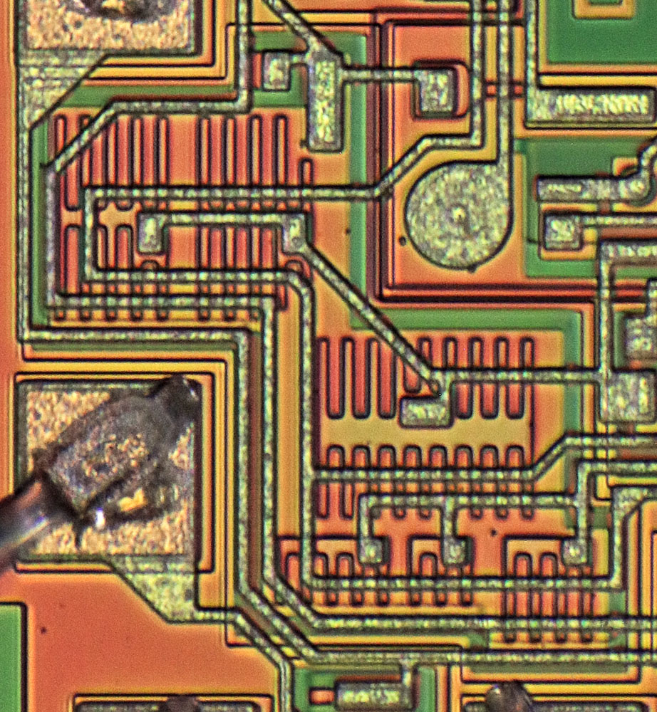
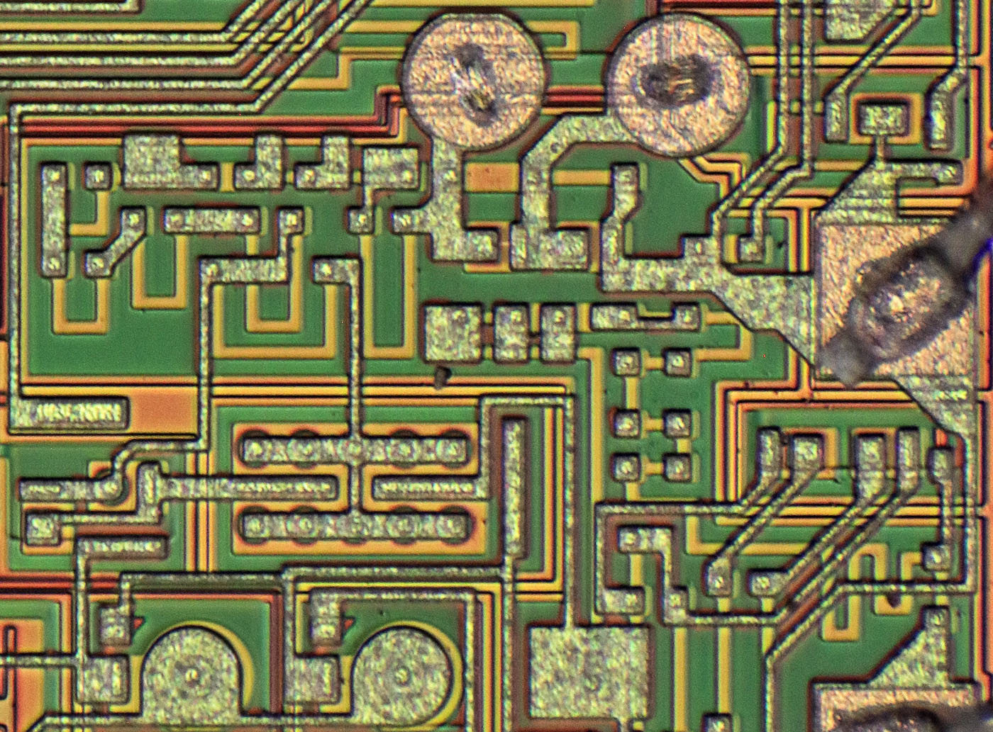
The capacitors are comb-shaped. They are emitter areas in areas with base doping. The special shape ensures higher capacitance because the emitter doping has a certain depth and the comb structure thus increases the surface area.
However, the base-emitter junction has a low breakdown voltage. For this reason, it was necessary to generate a higher auxiliary potential as reference potential for the capacitors.
 https://www.richis-lab.de/LM723_12.htm


