Hey guys,
I think this is something eevblog folks would appreciate. Check out my latest PCB business card! It's made out of 2 layer 0.8mm FR4.
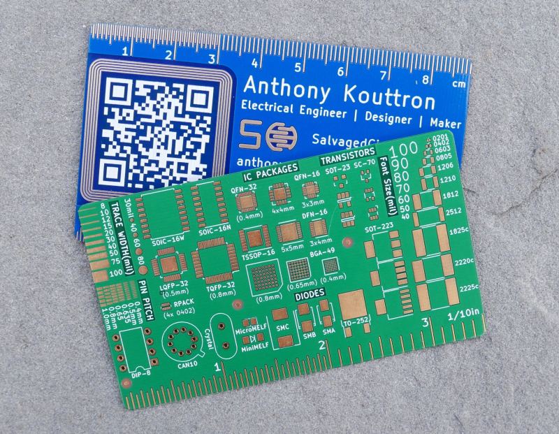
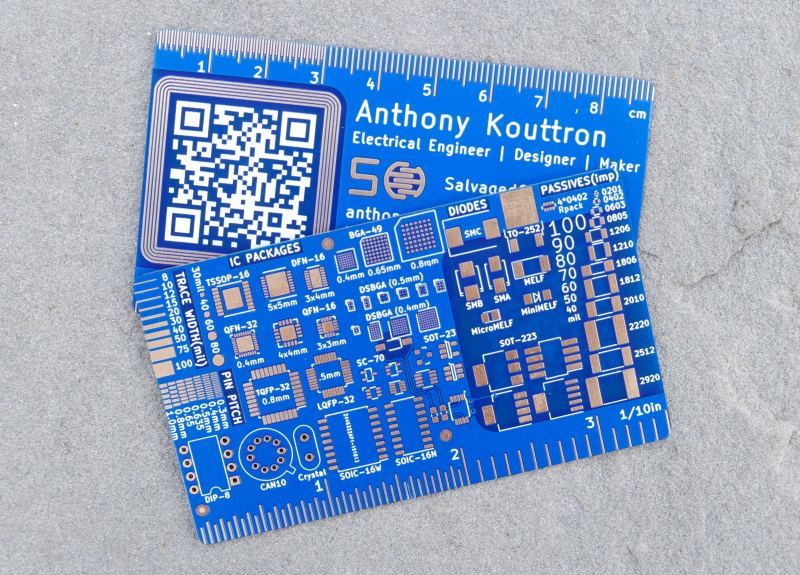
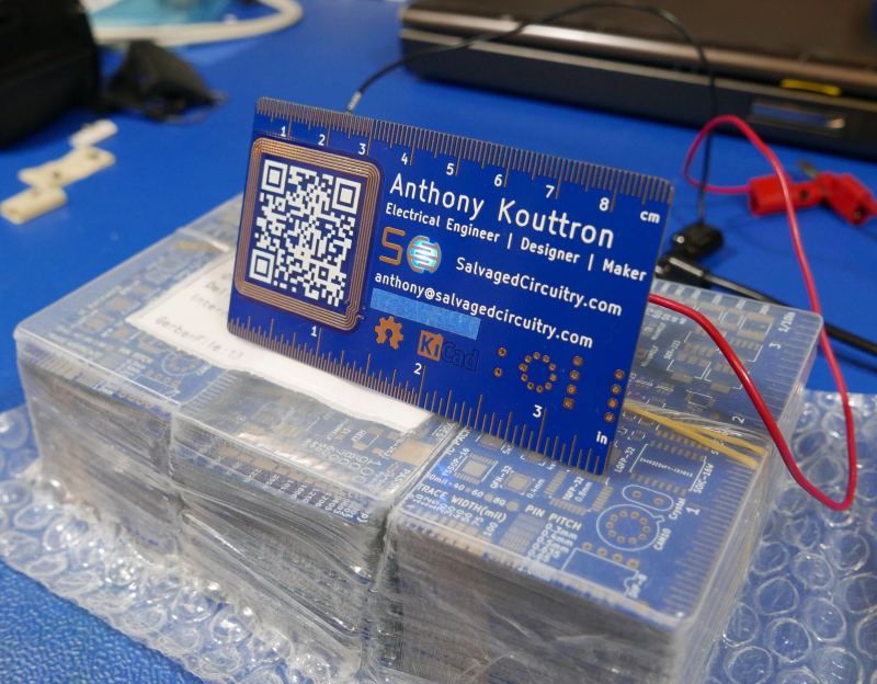
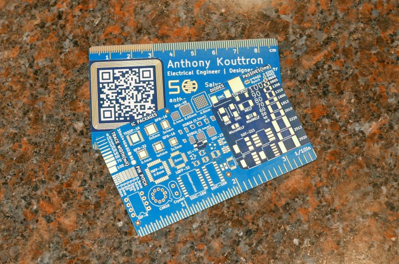
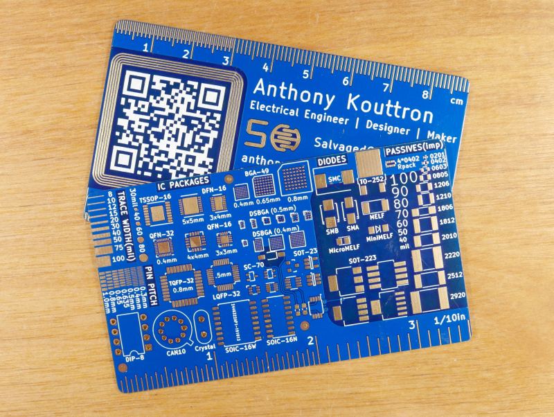
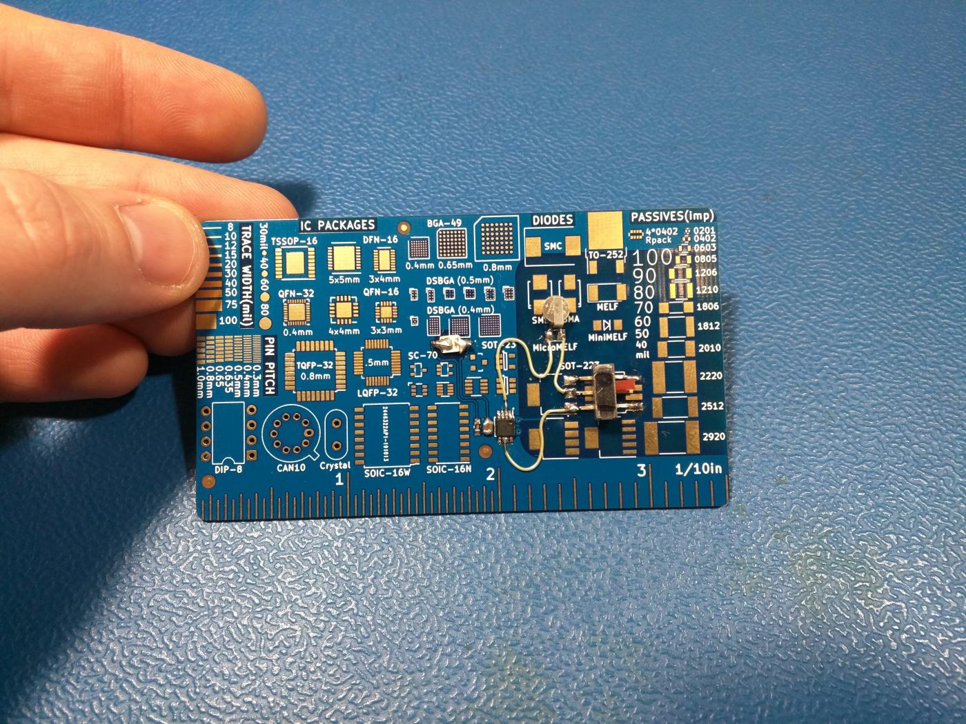
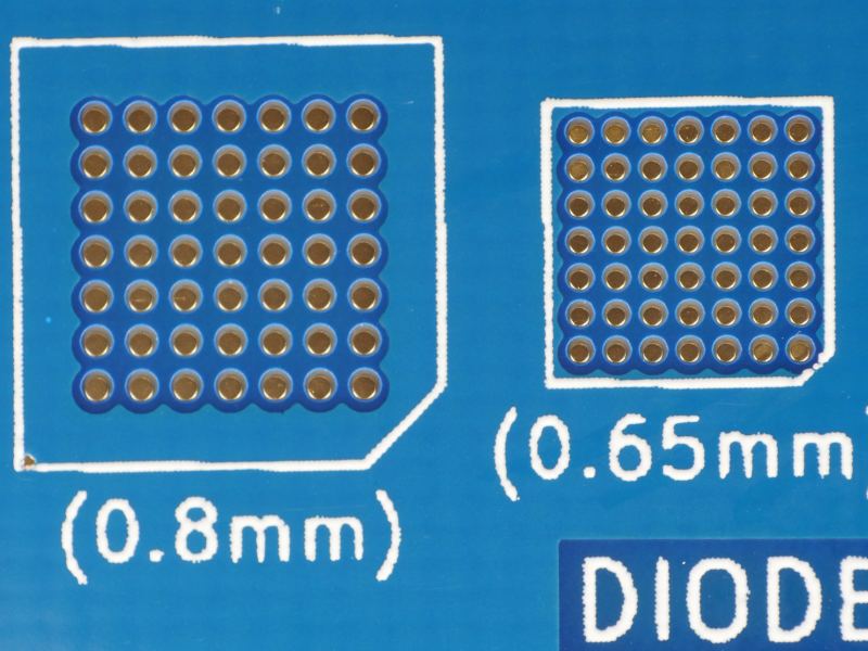
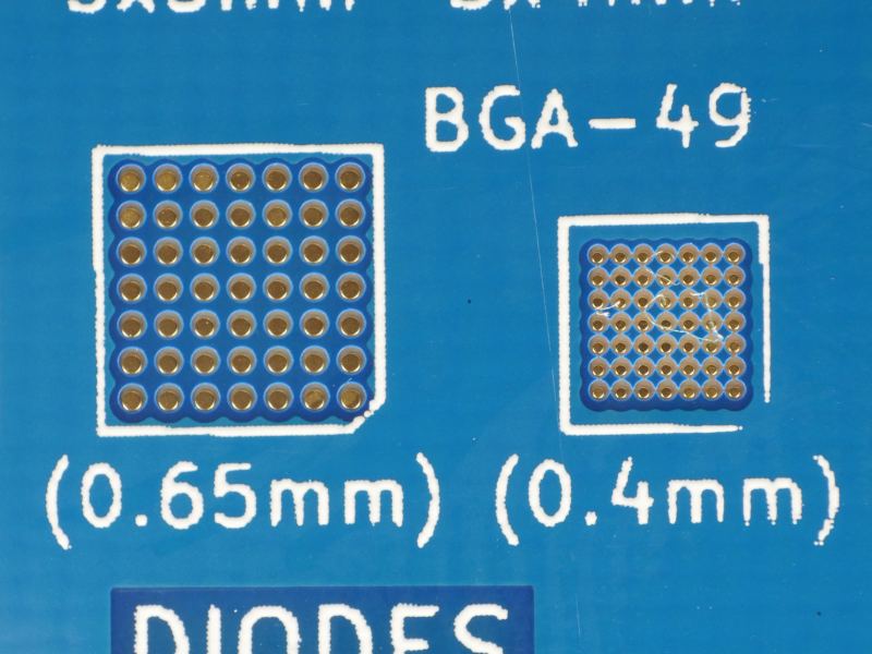
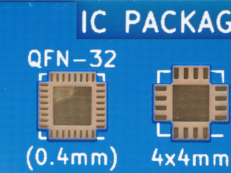
This business card has NFC capabilities and features the most common integrated circuit footprints found on circuit boards today. Three rulers of different measure are also included: 1/32in ruler, 1/5mm ruler, 1/10th ruler. A trace width and pin patch gauge are also included, along with the different resistor and diode package sizes. The good news, is it only cost me $0.66 each for 150 of em. That's not terrible considering paper business cards are $0.04-0.06 in quantities of 500. These are Electroless Nickel-Gold plated though. Can't beat that!
Here's a few shots:
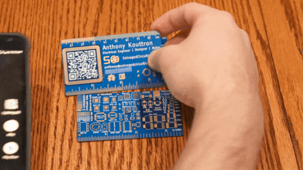
Business cards in action:
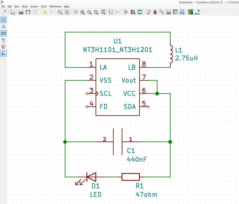
Circuit:
Layer stackup:
This card was designed in Kicad 5.0. Kicad is free pcb design software that is quite good. I used to use eagle cad to design small pcbs but Kicad now fills that need.
The PCB design files are free to modify for personal use and fall under a creative commons license.
PCB files to make your own are available here:
https://github.com/anthonykouttron/pcb-business-card-qr-nfcFor a complete detailed writeup check this out:
https://salvagedcircuitry.com/pcb-business-cardI'd love feedback from you guys. Let me know what you think!
I like the idea! Wouldn't mind it if someone gave me one instead of the old boring paper one. But I would never carry these around though, seems too bulky for my wimpy arms.
Your design looks very slick and I like the usability of it. Good Job!
I have been thinking about Designing something like that on my own for some time now, maybe not to give them away but to have one on my Desk for vanity purposes.

Have not gotten around doing it yet tho.
Suggestion, make it double as a soldering exercise. Instead of just footprints, make it do something and put a link in the QR somewhere that leads to assembly instructions.
Where is the chip? I don't see it anywhere.
Not mounted on picture I guess, it's on the backside.
Will be even nicer on a flex pcb
Not mounted on picture I guess, it's on the backside.
The chip and the 4 discretes... are nowhere to be found

How do i flash or write info to the xqfn-8 nfc chip?
Not mounted on picture I guess, it's on the backside.
The chip and the 4 discretes... are nowhere to be found
This is the side of the card that does the business.
One thing I greatly underestimated was the amount of light fall off from two layers of soldermask. I originally implemented a 400mcd reverse mount led to illuminate my logo on the top side. This was a farcry from the light output actually needed. I soldered in a high powered led and a tiny ml-421 lithium battery as a quick fix. I don't quite know what the mcd of the high powered led was, it was in a bag of random bright leds I had.
How do i flash or write info to the xqfn-8 nfc chip?
The NFC chip handles all communication via a paired NFC coil. So it can be completely programmed through "NFC tools" an android app for programming NFC chips. It can also be programmed via the NXP NFC android app.
Suggestion, make it double as a soldering exercise. Instead of just footprints, make it do something and put a link in the QR somewhere that leads to assembly instructions.
This is a great idea! I am in the process of making a cell-phone-repair edition of this business cards, so people who are practicing reballing / reflowing random Apple A-series chips and qualcomm arm chip alternatives have something to practice on. It will probably be a one-time-use thing as I don't think the tg-130 used in cheapo board houses will hold up very well to resoldering more than once (traces will pull up / tear). Debating whether it is better to have the bga pinouts break out or just let the end user band saw them in half to inspect the joints. Thanks for the great input guys!
Bonus: Who doesn't love a PCB manufacturer fight?
This is pcbway:
This is JLCpcb:
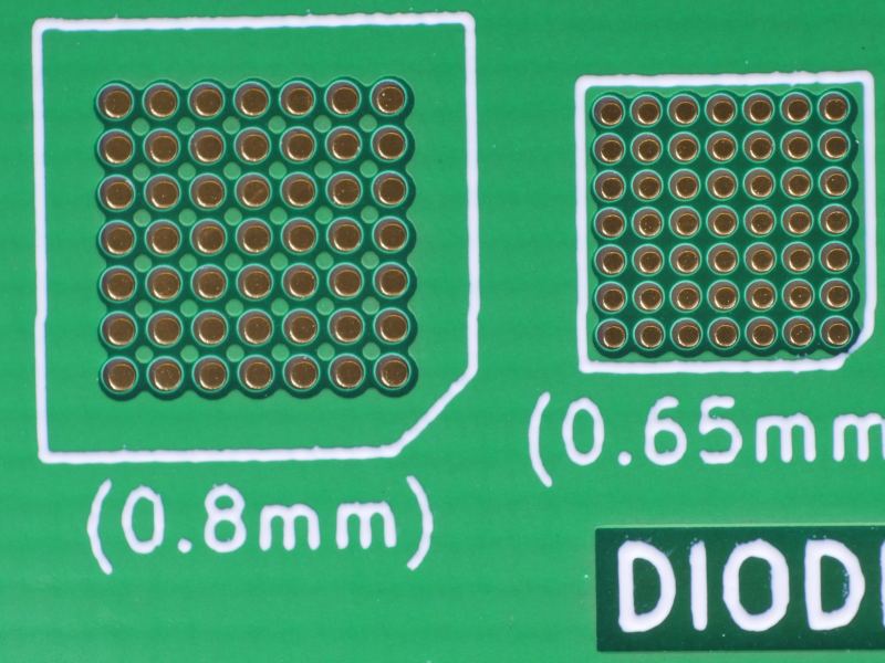
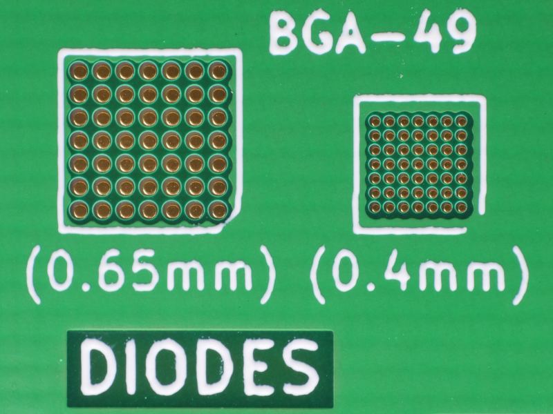
Both vendors have a very similar out-of-center tolerance, but the soldermask quality seems quite different. Granted, this is apples to oranges comparison. Pcbway green soldermask could be better. However, it seems that Pcbway doesn't bridge soldermask if an opening is less than 0.25mm or 0.2mm. These images are also not super flat as I was using a very cobbled-together setup. I finally got my hands on a macro, so better images incoming

I'm not part of any discount program with any pcb vendor and have not signed up for any "review" Discount / payoff.
I'm planning on sending these to OshPark and advanced circuits to check out their capabilities. I think both these vandors will have far better centering. Sure, it'll cost more, but I can't wait to find out.
You are using the 2 layer process right? The 4 layer process of JLCPCB is far better and this is true of probably all other boardhouses as well. The 2 layer process is built down to extreme cost and can't really be fairly compared to advanced circuits because they charge as much for 2 layer boards as JLC charges for 4 layer boards.
JLCPCB 0.2mm drills, 0.125mm annular ring:

0.4mm BGA pads:

JLCPCB 0.2mm drills, 0.125mm annular ring:
0.4mm BGA pads:
Wow, that is quite the improvement! Thanks for the photos. This is good information to know.