Author Topic: Transistors - die pictures  (Read 249319 times)

0 Members and 1 Guest are viewing this topic.

Offline magic

  • Super Contributor
  • ***
  • Posts: 7198
  • Country: pl
Re: Transistors - die pictures
« Reply #925 on: September 07, 2024, 05:40:16 am »
PNP Darlington transistor with an integrated free-wheeling diode
Hmm, where exactly is the diode supposed to be?
Is this... from eBay?
 

Offline NoopyTopic starter

  • Super Contributor
  • ***
  • Posts: 1886
  • Country: de
    • Richis-Lab
Re: Transistors - die pictures
« Reply #926 on: September 07, 2024, 05:54:00 am »


You can see it here. That´s not just a window in the passivation.
(https://www.richis-lab.de/Bipolar60.htm)


...or here...
(https://www.richis-lab.de/Bipolar59.htm)


I have done IR pictures and they show IR light exactly in this area. It all makes sense.


Someone has sent the part to me. I don´t know the history but it doesnt look like a fake to me.
 
The following users thanked this post: magic

Offline NoopyTopic starter

  • Super Contributor
  • ***
  • Posts: 1886
  • Country: de
    • Richis-Lab
Re: Transistors - die pictures
« Reply #927 on: September 10, 2024, 03:07:11 am »


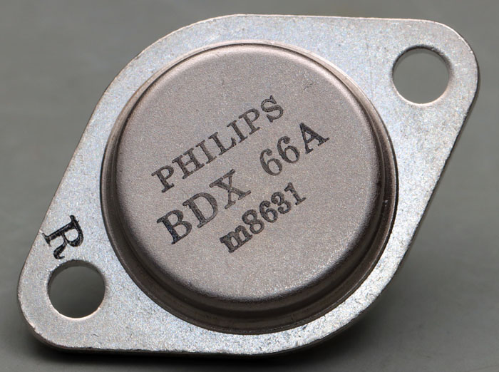
BDX66, now built by Philips. Same specifications...


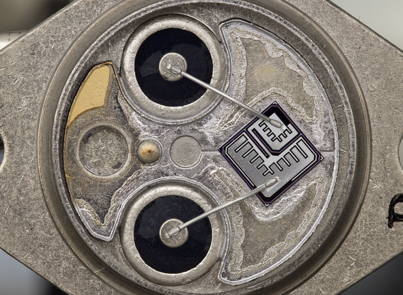
The package contains a very large die on a large heatspreader.


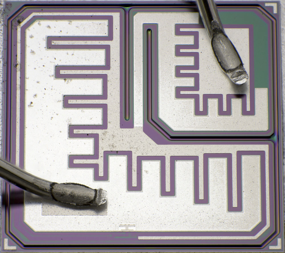
The edge length of the die is 5,0 mm. The surface appears to be dirty in the top left-hand corner.


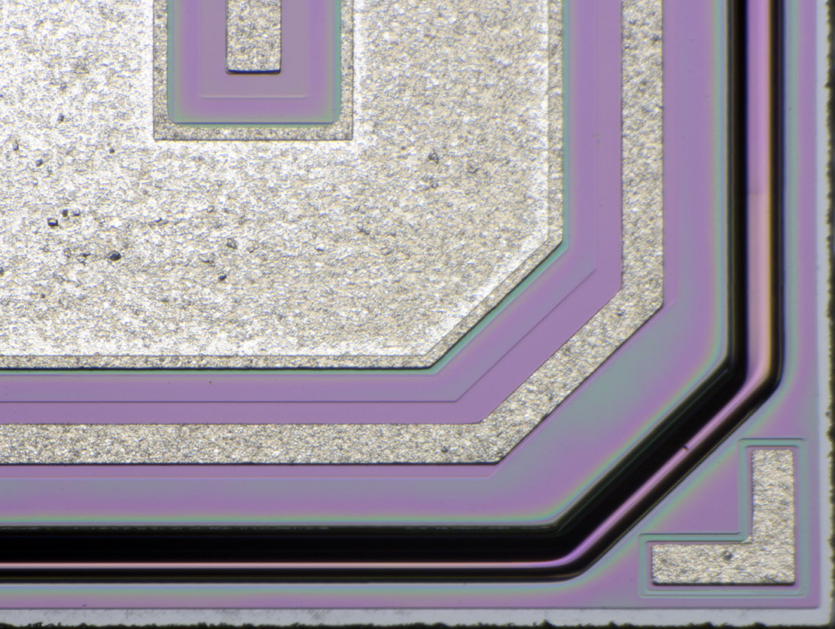
The MESA trench has been inserted extremely cleanly into the die.


As shown in more detail for the MJ3001 (
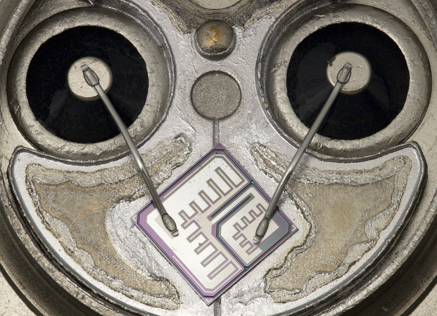
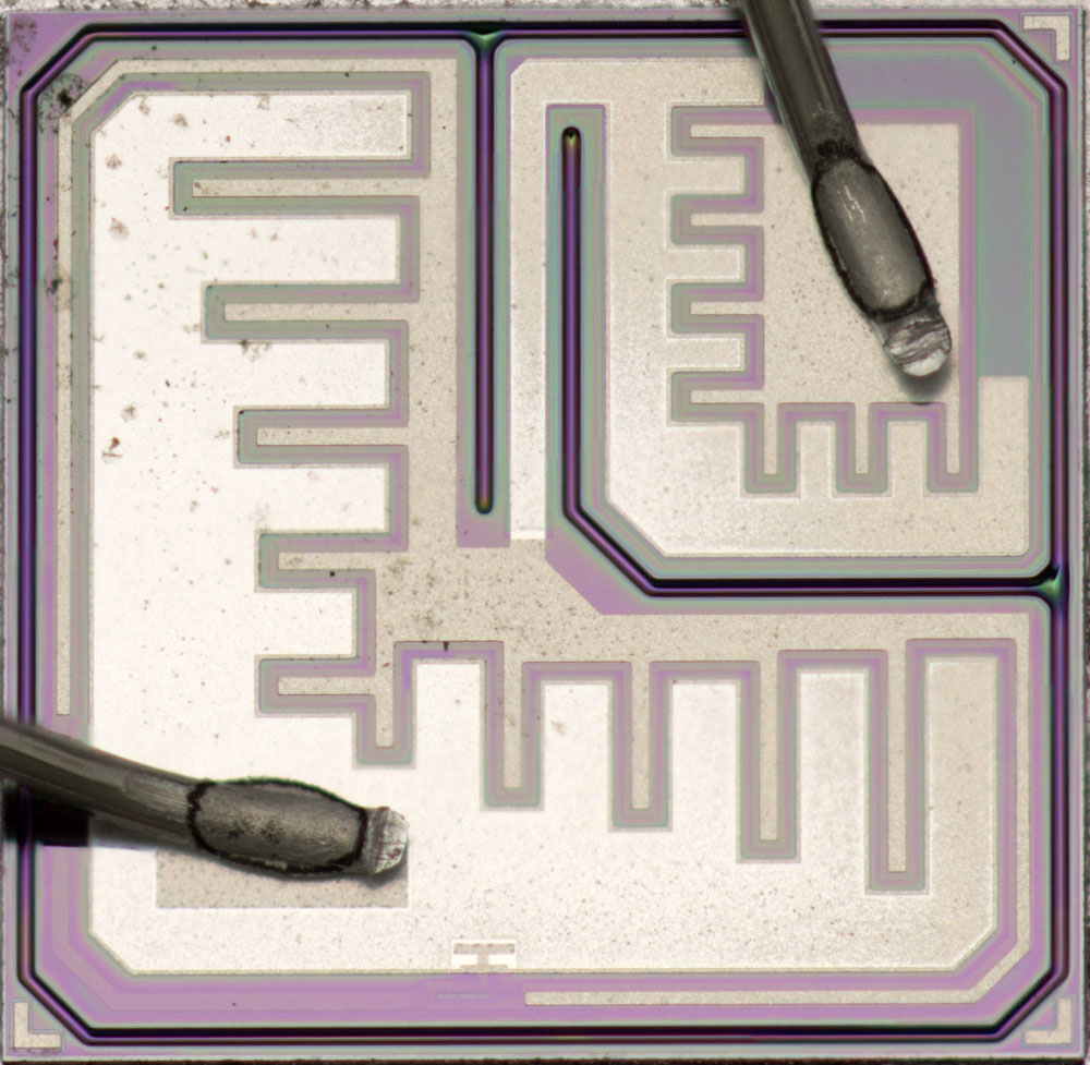
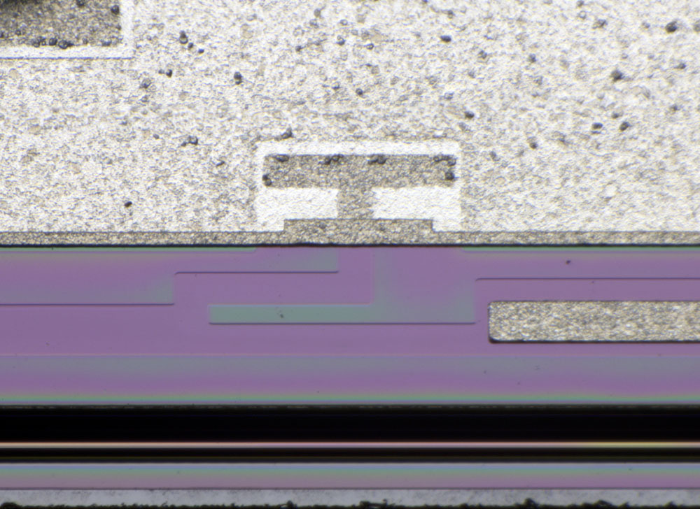
https://www.richis-lab.de/Bipolar60.htm), a line runs as a resistor across the left-hand side of the die from the base to the emitter of the power transistor. The unusual contact area at the lower edge is interesting...


https://www.richis-lab.de/BipolarA65.htm

 :-/O
 
The following users thanked this post: RoGeorge, ch_scr


Share me

Digg  Facebook  SlashDot  Delicious  Technorati  Twitter  Google  Yahoo
Smf