In my "Homebrew analog computer" thread I mentioned a couple of times that I am planning to build a work-alike to the PDP-8 digital computer. My analog computer construction is temporarily on the back burner again as I wait for a batch of PCB's and semiconductors to arrive. In the meanwhile I have been working on an off on the design of the digital machine. I've done a reasonable amount of prototyping on the bench to verify the constructional blocks of the machine and have the complete specification sorted out. Most of the logic flow diagrams are also worked out.
It's going to be a 12-bit machine with 4096 words of 12-bit memory but a reduced version of the PDP-8's instruction set. One of the "building blocks" I am currently working on the the universal bidirectional 12-bit shift register, for the machines accumulator and program counter. With the exception of the computers memory, the circuitry is going to be entirely discrete transistor.
The heart of the register is 12 clocked data-input, edge triggered flop-flops with control and signal steering logic. The data-flop flops themselves are reasonably complex; each flop-flop consisting of coupled slave and master R-S flop-flop with steering logic to give an edge triggering capability to the clock input that is wholly insensitive to propagation delays. The slaved R-S flop-flop forms a memory element for the data present at the instant of the clock edge.
Here is screen shot of the complete simulation I have up and running of the shift register:

And here it is in operation:

At t=1.3mS the serial data input (second trace from the top) goes high for three clock periods. Consequently 3 active-high bits are shifted through the 12 bits of the register at each successive clock interval. At t=2.7mS, one clock cycle before the last bit is shifted out of the register, the shift-left control input is asserted (third trace from the top) and the data bit is shifted through the register in the opposite direction. This shift register is in fact a universal design which is parallel-programmable, with 12 parallel preset inputs (P0 through P11) in addition to the 12 parallel data outputs (D0 through D11). In the simulated case here the P0-P11 inputs are wired to the D0-D11 inputs to give the reverse ("left") shifting capability (Q1 to P0, Q2 to P1, Q3 to P2, Q4 to P3, etc...)
So here you have the mechanism for the micro-instructions RAL and RAR - rotate accumulator left and rotate accumulator right.
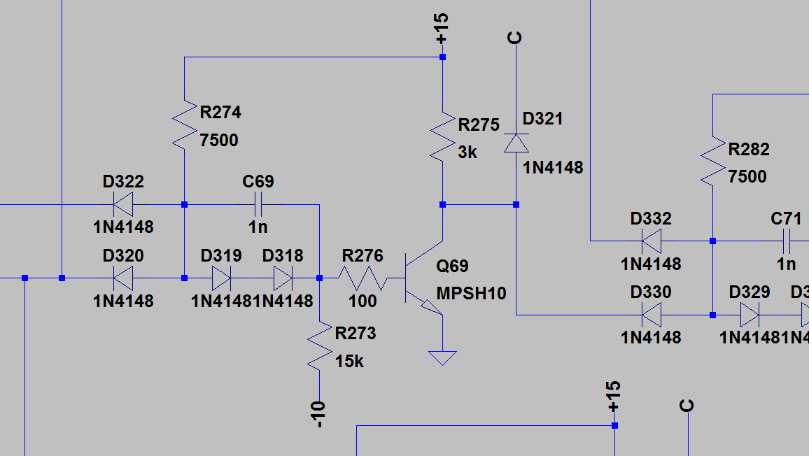
One thing to note is that the entire register (as well as nearly all of the rest of the computers logic) is constructed with a 2 basic building blocks - NAND gates and inverters!:

The universal inverter stage is identical to the universal NAND gate, minus an input diode.
Of course all of the above constitutes only a very small part of the project. ATM I am finalizing a PDP-1-like front panel layout for the control console, to send off to Front Panel Express. If there is sufficient interest in such a project I may keep this thread updated as i plod along, perhaps starting next with the machines specification and layout and logic diagram of the shift-resister and the clocked data flip-flops, when I have some more spare time......