Author Topic: Electronic Load Project - TLV171 & IRFP250 with KiCad Files  (Read 50892 times)

0 Members and 1 Guest are viewing this topic.

Online Kleinstein

  • Super Contributor
  • ***
  • Posts: 14651
  • Country: de
Re: Electronic Load Project - TLV171 & IRFP250 with KiCad Files
« Reply #175 on: January 12, 2020, 09:38:37 am »
The shown scope traces are with a rather fine time scale. The visible "frequency"  is thus rather high - higher than expected for oscillations of the OP. Also it does not look like a single frequency, more like noise or EMI (e.g. FM radio).  This could be coupled to the circuit or as well picked up by the ground wire of the probe.  Chances are there could be a similar level without the circuit or just from the supply / mains.

If it is really related to the circuit it would be more like a slightly larger gate resistor. The OP is likely not fast enough.
Chances are the circuit is OK as it is.

For a small heat sink with fan the temperature rise is not that bad. At some point there is not much sense in improving the heat sink, as there is also thermal resistance in the FET itself and the case to heat sink interface. So a little more is OK, but not much more is needed with a fan.

It could be time to think about the extra circuit to limit saturation with the FET all the way on. This is already beyond the normal electronic load, but it would absolutely make sense to avoid possible spikes o turn on. My idea would be to add some kind of switch over to a constant resistance mode if the voltage is too low. This is a little like the CV to CC mode switch over in a lab supply. So if the voltage is too low, the current setting gets reduced to a level about proportional to the voltage. With an an adjustable limit this may also work as a constant resistance mode. Existing circuits for resistance emulation may be a good starting point.


The following users thanked this post: t1d

Offline t1dTopic starter

  • Super Contributor
  • ***
  • Posts: 1248
  • Country: us
Re: Electronic Load Project - TLV171 & IRFP250 with KiCad Files
« Reply #176 on: January 12, 2020, 11:32:41 pm »
Thanks, Kleinstein,

My expectation was that the next step was to test the circuit using the inductor that I built for that purpose. If we just missed that, what are the test perimeters? The same as the last test, but add the inductor?

As for designing a current limiter...
1) The MOSFET did not saturate even at the full design goal voltage and current; 30V @ 2A = 60W. However, because of the MOSFET's increasing heat, the circuit only remained at this level for a moment, or two. And, no auxiliary oscillation was injected.
2) Designing a CC circuit is above my present pay grade. But, maybe one day...
 

Offline t1dTopic starter

  • Super Contributor
  • ***
  • Posts: 1248
  • Country: us
Re: Electronic Load Project - TLV171 & IRFP250 with KiCad Files
« Reply #177 on: February 09, 2020, 01:02:48 pm »
Inductance Test
Feb 9th/2020

Purpose
To add inductance in series with the positive leg of the load and observe the circuit’s reaction.

Setup
Probe #1 – Yellow – Attached to MOSFET input pin. A 15.0mV offset may have been left on, throughout testing.
Probe #2 – Purple – Attached to shunt resistor input pin.
38.38uH of inductance was added in series with the load on the positive leg.
Beginning ambient temperature 22-23*C.
The current setting of the circuit was determined with a separate DMM.
The face temperature of the MOSFET was determined with a separate DMM.
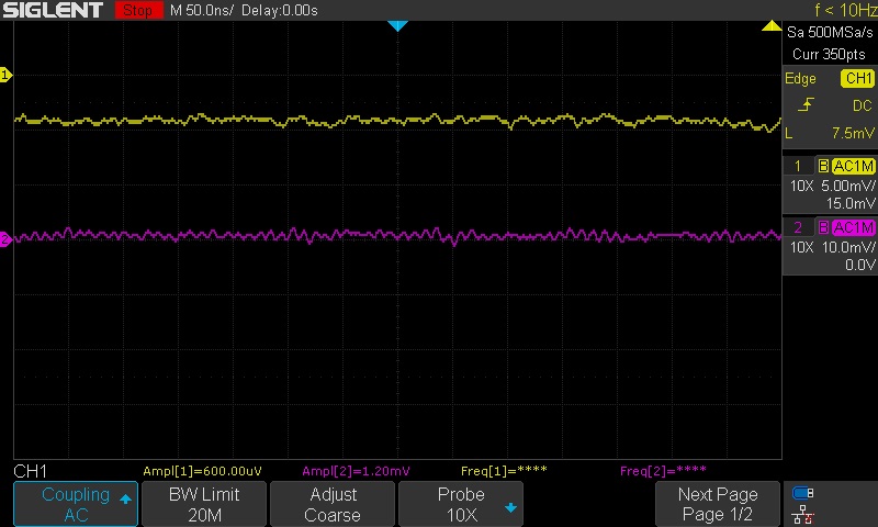
Ambient Noise
This picture was taken after the end of the first test level. The test system was left fully in place and the only change made was that the PSU supply was switched to standby.


First Level of Testing
PSU set to 10.0v and 1.4a. The addition of 0.40a was added to test for circuit advancement beyond the circuit’s current setting of 1.0a.
Circuit set to 1.0a
Soak time = 30 minutes
MOSFET face temperature revolved around 35*C, with minor variations.


Second Level of Testing
PSU set to 30.0v and 2.4a. The addition of 0.40a was added to test for circuit advancement beyond the circuit’s current setting of 2.0a.
Circuit set to 2.0a
Soak time = 30 additional minutes
MOSFET face temperature revolved around 108*C, with minor variations.


Observations
Both positive and negative amplitude variations were observed at both test levels. They manifested as signal jumps, being whole lines, or slopes. It is important to note that these events were not spikes. The current sunk remainded steady and had only minor float.

I am not experienced enough with my scope to collect the max/min data through the scope’s functions. But, I did try to use the max/min settings and I was able to see 400mV readings, most often, during the instantaneous fluctuations. This same 400mV reading was observed with the supply set to standby, but it occurred as spikes. I am not saying that the maximum reading was 400mV, only that it occurred enough for me to see it among the flashes.

Conclusion
The jumps in amplitude will be investigated. I think my new scope can record a session. If so, I will repeat the test and make a movie.

My guess is that the jumps in amplitude may be a build up and collapse of the inductance? This is beyond my present knowledge, but I am sure Kleinstein can set us straight.

I would think that the majority of the noise observed is from ambient sources.

The results are encouraging. With the circuit at its full design limits, 30v/2a/60w and with inductance added, the circuit yielded these results…
- Steady current sinking operations.
- Low noise.
- Low MOSFET face temperature

We are, again, in need of Kleinstein’s wisdom and knowledge… To draw conclusions from the above… And, to determine what needs to be done next.

One additional thought… I have recently learned about current mirrors and I wonder if one might be useful to balance the load between the two MOSFETs, in the Dual MOSFET model.

« Last Edit: February 09, 2020, 01:20:29 pm by t1d »
 

Online Kleinstein

  • Super Contributor
  • ***
  • Posts: 14651
  • Country: de
Re: Electronic Load Project - TLV171 & IRFP250 with KiCad Files
« Reply #178 on: February 09, 2020, 01:28:03 pm »
The inductance could effect the response to things like steps in the DUT voltage, as this is the difficult load case. I would expect the circuit to behave well. So the test is more like just in case and to make sure it really does. From the scope pictures it is hard to tell if this is just noise / external picked up interference.

For better visibility one could try adding some jumps to the set current, e.g. make the load go 0.5 A to 0.6 A and back. The active steps in the current are a little different from an external disturbance, but not to much. Such load jumps could also be a good test for a regulator, though the more normal way it with 2 separate loads and switching on hard on / off.
 

Offline t1dTopic starter

  • Super Contributor
  • ***
  • Posts: 1248
  • Country: us
Re: Electronic Load Project - TLV171 & IRFP250 with KiCad Files
« Reply #179 on: February 09, 2020, 01:41:29 pm »
Thanks, Kleinstein!
How about a square wave, through the auxiliary input. Would that do it? If so, what frequency/amplitude/etc... My Function generator only goes to 2MHz and I think the max amplitude drops to 10Vpp.

Edit: Oops... We are talking about switching the current. So, yes, my PSU has two channels and I can switch between them. I will do the test and report back. Thanks!
Edit2: Hmm..  I think this will require learning how to set up the PSU to trigger. I will need to tie the scope to it, to catch the change. Sounds like lots of fun...
« Last Edit: February 09, 2020, 01:46:27 pm by t1d »
 

Online Kleinstein

  • Super Contributor
  • ***
  • Posts: 14651
  • Country: de
Re: Electronic Load Project - TLV171 & IRFP250 with KiCad Files
« Reply #180 on: February 09, 2020, 02:53:40 pm »
The external set input and function generator is perfect for the test. I would try it with a square, at low frequency (e.g. 100 Hz - 1 kHz) and something like 0.5 /0.6 A, so not all the way to zero and not full current.
 

Offline t1dTopic starter

  • Super Contributor
  • ***
  • Posts: 1248
  • Country: us
Re: Electronic Load Project - TLV171 & IRFP250 with KiCad Files
« Reply #181 on: February 09, 2020, 06:06:58 pm »
The external set input and function generator is perfect for the test. I would try it with a square, at low frequency (e.g. 100 Hz - 1 kHz) and something like 0.5 /0.6 A, so not all the way to zero and not full current.
My Function Generator only has an adjustable voltage. The current is fixed and the (short) instructions do not say what it is. See picture.


However, my new PSU does have a Timer output that allows you to select voltage, current and timer intervals. See picture.


With either instrument, I will need to learn how set up my new oscilloscope to trigger and how to connect all the instruments. But, I am determined to work it out.

Thank you for your support and help.
« Last Edit: February 09, 2020, 06:12:46 pm by t1d »
 

Online Kleinstein

  • Super Contributor
  • ***
  • Posts: 14651
  • Country: de
Re: Electronic Load Project - TLV171 & IRFP250 with KiCad Files
« Reply #182 on: February 09, 2020, 06:18:30 pm »
Of cause the Fgen has a voltage output. It is the job of the electronic load to convert from control voltage to current.  This may need an offset to the output at the Fgen. So something like 0.5 / 0.6 V from the generator if the load gives 1 A/V.
 

Offline t1dTopic starter

  • Super Contributor
  • ***
  • Posts: 1248
  • Country: us
Re: Electronic Load Project - TLV171 & IRFP250 with KiCad Files
« Reply #183 on: February 09, 2020, 06:32:51 pm »
Of cause the Fgen has a voltage output. It is the job of the electronic load to convert from control voltage to current.
Sorry, no sleep, yet again, and your prior message said "0.5/0.6 A." 
This may need an offset to the output at the Fgen. So something like 0.5 / 0.6 V from the generator if the load gives 1 A/V.
I will repeat your instructions, so I can make sure that I understand... Set the voltage amplitude of the Function Generator to 0.5/0.6V and its square wave frequency to 100 - 1KHz. Set the electronic load to 1 amp per volt. Do I have it correctly now?
 

Online Kleinstein

  • Super Contributor
  • ***
  • Posts: 14651
  • Country: de
Re: Electronic Load Project - TLV171 & IRFP250 with KiCad Files
« Reply #184 on: February 09, 2020, 08:56:48 pm »
The Fgen should be more like 0.1 V (peak to peak) amplitude and a 0.55 V (or similar) offset. So the voltage would change between some 0.5 and 0.6 V. The offset could be from the Fgen or maybe from the load circuit if it permits.

The 0.5 and 0.6 A value was meant for the resulting current of the load and not the FGen. Sorry for the confusing text.
 

Offline t1dTopic starter

  • Super Contributor
  • ***
  • Posts: 1248
  • Country: us
Re: Electronic Load Project - TLV171 & IRFP250 with KiCad Files
« Reply #185 on: February 09, 2020, 09:53:42 pm »
The Fgen should be more like 0.1 V (peak to peak) amplitude and a 0.55 V (or similar) offset. So the voltage would change between some 0.5 and 0.6 V. The offset could be from the Fgen or maybe from the load circuit if it permits.
I think I have it, now. Thank you for the extra explanation.

The 0.5 and 0.6 A value was meant for the resulting current of the load and not the FGen. Sorry for the confusing text.
No worries, at all. You are very gracious with your time, knowledge, effort and expertise. And, you are very patient with my lack of knowledge. Thank you!

Amazingly, we have come a long way and made good progress. I think we are close to being able to say we have a complete project and that it works well. Your design is proving to be very robust.
 

Offline t1dTopic starter

  • Super Contributor
  • ***
  • Posts: 1248
  • Country: us
Re: Electronic Load Project - TLV171 & IRFP250 with KiCad Files
« Reply #186 on: February 09, 2020, 10:10:18 pm »
I checked and the function generator does have an offset. So, I will report back to you, when I have completed the test. Thanks.
 

Offline t1dTopic starter

  • Super Contributor
  • ***
  • Posts: 1248
  • Country: us
Re: Electronic Load Project - TLV171 & IRFP250 with KiCad Files
« Reply #187 on: February 11, 2020, 12:29:35 am »
Setups

E_Load
Voltage = 1V
Amperage = 1.0A

DUT = PSU
Voltage = 1V
Amperage = 1.1A (0.1 added to look for drift.)

Function Generator
Wave Type = Square
Frequency = 501.16 ~ 501.22Hz (The drift is due to the age of the unit.)
VPP = 584mV (This is the units minimum setting.)
Offset – +0.50V
Impedance = 600 Ohms

Oscilloscope
Both Test Probes = x10/20MHz
Probe 1 – Yellow = Attached to a fly-wire soldered to the board at the MOSFET Gate.
Probe 2 – Purple =  Attached to the input of the Shunt Resistor.
BNC Lead Ch 3 = x1/20MHz. Was attached after testing to take picture to show the Function Generator waveform.

MOSFET Face Temperature
Was monitored with a separate multimeter.

Environment
The florescent light bulb that is on the same house circuit was turned off for these tests.

Results
The E-Load performed as expected. The current was sunk steadily and consistently. The waveform was transformed to a triangular shape, but was not degraded.

The auxiliary input worked as expected.

The MOSFET’s face temperature rose less than 2*C above ambient.

I am well pleased with the results.

Kleinstein, what do you see?
What needs to be corrected and how?
What are your instructions for what to do next?
Thank you so much for your contributions to the project. I am having great fun and I hope you are too.

Picture 1 - Yellow = MOSFET Gate


Picture 2 - Purple = Shunt Resistor Input


Picture 3 - Function Generator Waveform
« Last Edit: February 11, 2020, 12:34:36 am by t1d »
 

Online Kleinstein

  • Super Contributor
  • ***
  • Posts: 14651
  • Country: de
Re: Electronic Load Project - TLV171 & IRFP250 with KiCad Files
« Reply #188 on: February 11, 2020, 07:17:53 am »
The gate waveform looks more like triangle and not much visible at the shunt.  The triangle waveform points towards a low bandwidth somewhere. If this is before the control loop, one could change this. The control loop is not very fast, but I expect a higher speed. Anyway one could lower the frequency for a start to see at least something that is similar to a square at the gate.
For the test I would use a little more than 1 V from the supply, more like 5 V to give the load something to work with. If available a larger series resistor (e.g. at the negative side to the supply) one could see the current with higher resolution. To limit the power one may chose a lower current range (e.g. 50 mA - 100 mA).
 

Offline t1dTopic starter

  • Super Contributor
  • ***
  • Posts: 1248
  • Country: us
Re: Electronic Load Project - TLV171 & IRFP250 with KiCad Files
« Reply #189 on: February 27, 2020, 06:39:24 am »
... Anyway one could lower the frequency for a start to see at least something that is similar to a square at the gate. For the test I would use a little more than 1 V from the supply, more like 5 V to give the load something to work with.
If available a larger series resistor (e.g. at the negative side to the supply) one could see the current with higher resolution. To limit the power one may chose a lower current range (e.g. 50 mA - 100 mA).
I did a new test and tried to match your setting instructions. See the following post.

I did the test without the additional series resistor on the negative side of the supply. I need your instructions as to what resistor(s) to use. In power resistors, I have available:
(4 Each) 1R/10%/5W
(2 Each) 10R/5%/5W
(1 Each) 220R/5%/5W
 

Offline t1dTopic starter

  • Super Contributor
  • ***
  • Posts: 1248
  • Country: us
Re: Electronic Load Project - TLV171 & IRFP250 with KiCad Files
« Reply #190 on: February 27, 2020, 06:48:39 am »
Setups
Function Generator:
101Hz/VPP=5.20/Offset=+0.92v/Termination=50R

Scope:
For a picture of the Function Generator Setup(Picture 4): Channel 3/Blue/BNC Cable = x1/BWL=20M/DC Coupled

Probes:
Channel 1 – Yellow/x10/BWL=20M/DC Coupled/Gate Pin
Channel 2 – Purple/x10/BWL=20M/DC Coupled/Shunt Resistor Input

DUT:
PSU= 5V/0.14A (0.04A added to detect drift)

E-Load:
The Function Generator was removed from the scope and was connected to E-Load auxiliary input.
The DUT was connected to E-Load through the 38.38uH Inductor.
The E-Load was set to sink 0.11A

Picture 5 – Probes DC Coupled
Channel 1 shows the waveform at the Gate Pin. The waveform is already beginning to deform at this slow speed.
Channel 2 shows noise on the Shunt Resistor pin. See Picture 7 for additional findings on Shunt Resistor Input.

Picture 7 – Probes AC Coupled
I switched the coupling to AC, just to see what was there. That’s when I realized that there is a ring on the Shunt Resistor Pin concurrent with the change of direction of the waveform – rising to falling and falling to rising. This ring is 14.2mV in amplitude.

Conclusions:
The E-Load sunk the load steadily throughout the test.
The MOSFET face temperature remained just a degree, or two, above ambient.
The deformation of the waveform should be investigated and improved to higher frequencies.
The ring on the Shunt Pin Input should be investigated further and cured, if it is considered significant.

As always, Klienstein, I need your directions for what to do next and specifically how to set it up. Thank you, good sir.


« Last Edit: February 27, 2020, 06:52:06 am by t1d »
 

Online Kleinstein

  • Super Contributor
  • ***
  • Posts: 14651
  • Country: de
Re: Electronic Load Project - TLV171 & IRFP250 with KiCad Files
« Reply #191 on: March 07, 2020, 10:01:33 pm »
The gate voltage signal looks reasonable, though relatively slow. Anyway better to start a little slow than oscillating. So if the measurement of the current is OK, one could consider a speed up with slightly smaller capacitors. One could also compare the measurement to a simulation. The simulation could than give a hint on how small the capacitor can be.

There seem to be some RF background on the signal at the shunt. However this signal looks more like coupled from the outside than with an origin in the circuit. The amplitude is changing at more random times, not related to the signal.
To really see the signal one could have another resistor in the current path (could be at the negative side) a larger resistor in the 10 Ohms range should give more signal and still not too much power to heat up the resistor too much.
 

Offline t1dTopic starter

  • Super Contributor
  • ***
  • Posts: 1248
  • Country: us
Re: Electronic Load Project - TLV171 & IRFP250 with KiCad Files
« Reply #192 on: March 07, 2020, 10:49:28 pm »
Thanks, Kleinstein!
The gate voltage signal looks reasonable, though relatively slow. Anyway better to start a little slow than oscillating. So if the measurement of the current is OK, one could consider a speed up with slightly smaller capacitors.
I am sorry to be so unlearned, but I need you to tell me which caps and what values to try.

One could also compare the measurement to a simulation. The simulation could than give a hint on how small the capacitor can be.
I have not learned to do simulations, yet. Maybe someone following the thread could contribute that for us.

To really see the signal one could have another resistor in the current path (could be at the negative side) a larger resistor in the 10 Ohms range should give more signal and still not too much power to heat up the resistor too much.
I believe that I have enough directions to do this part, on the next round of tests.

I do appreciate you so much!
 

Offline t1dTopic starter

  • Super Contributor
  • ***
  • Posts: 1248
  • Country: us
Re: Electronic Load Project - TLV171 & IRFP250 with KiCad Files
« Reply #193 on: June 16, 2020, 02:15:04 am »
This post will be about where the project stands, at present, and what I intend to do to wrap it up...

Testing of the Single-MOSFET design stopped in March, without necessarily being considered as completed. However, I have been using the test rig in regular use and find that...
1) It meets the design goals to be able to sink 2A/30V/60W. Actually, I think it can handle more than that. The MOSFET has never heated up to its rated limit, even with the poor heat sink and fan.
2) It has never saturated the MOSFET, gone into oscillation, or exhibited other errant behavior.
3) It has never caught on fire. lol...

This is not to say that my occasional use has adequately proven all functions. The Auxiliary (Function Generator) Input has never been used, for example. I will leave it to each individual that wants to build the device to make their own tests and conclusions. However, the Dual-MOSFET board is laid out better and should be even more robust.

To complete the project, several things need to be done to the Dual-MOSFET design...
1) Consider if the Dual-MOSFET design needs any additional circuitry to balance the load between the two sets of circuits. I really need the group's input, on this point.
2) Add Test Points to the PCB.
3) Change the Voltage Regulator specifications from the LM7(8&9) series to regulators that have more current output. This is just a precaution. It does not require any changes to the PCB.
4) Order the PCBs and build one out.
5) Do a little testing.
6) Change out the errant power supply in the permanent case, for the one that I have been using and know to work without terrible oscillations.
7) Install the PCB and heat sink in the permanent case.
8.) Remove the case from the kitchen counter, where it has been sitting all this time, and put it in the lab. :-DD

I have attached the Dual-MOSFET schematic, here, to save hunting for it in the earlier posts. The additional balancing circuitry is pending, of course. I am eager to hear from you, in that regard.

EDIT: I have discovered that the Voltage Reference circuitry is incorrect. See the additional image, for the needed correction. I will post the updated files, after further testing reveals any additional errors.


« Last Edit: January 27, 2021, 11:06:21 am by t1d »
 

Online Kleinstein

  • Super Contributor
  • ***
  • Posts: 14651
  • Country: de
Re: Electronic Load Project - TLV171 & IRFP250 with KiCad Files
« Reply #194 on: June 16, 2020, 07:16:33 am »
There is no need for some extra circuit to get precision balancing. There may be a small difference according to the OPs offset (likely some 10-100 mA), but this should be Ok and only a small part of the possible capacity.


There are a few possible additions one could consider:
1)  some temperature sensing and emergency off in case of too much.
2)  provision to sense the output voltage (high resistance divider)
3) together with 2) possibly a way to limit the current when the voltage drops too far. This could be a kind of constant resistance more that takes over. This would be a little like the CV/CC mode in a lab supply: one the voltage drops to far and this the effective resistance to low, there is a minimum resistance (e.g. some 0.2 Ohms here). So the load would be constant current / constant resistance. This extra part would avoid possible overshoot from MOSFET saturation / wind-up.
 
The following users thanked this post: t1d

Offline t1dTopic starter

  • Super Contributor
  • ***
  • Posts: 1248
  • Country: us
Re: Electronic Load Project - TLV171 & IRFP250 with KiCad Files
« Reply #195 on: June 16, 2020, 04:11:35 pm »
Kleinstein, it is wonderful to hear from you!

There is no need for some extra circuit to get precision balancing. There may be a small difference according to the OPs offset (likely some 10-100 mA), but this should be Ok and only a small part of the possible capacity.
That makes sense.

There are a few possible additions one could consider:
1)  some temperature sensing and emergency off in case of too much.
2)  provision to sense the output voltage (high resistance divider)
3) together with 2) possibly a way to limit the current when the voltage drops too far. This could be a kind of constant resistance more that takes over. This would be a little like the CV/CC mode in a lab supply: one the voltage drops to far and this the effective resistance to low, there is a minimum resistance (e.g. some 0.2 Ohms here). So the load would be constant current / constant resistance. This extra part would avoid possible overshoot from MOSFET saturation / wind-up.
Those are all really good suggestions. But, designing them is beyond my skills. Maybe someone will take up the project, where we have left off. All of your great technical advise and my KiCad files should give them a great head-start.

I did look at the current draw for doubling the circuit, in consideration of the 1 amp supply of the 7809/7909. Even doubled, the circuit draws very little. No worries. And, the 12V supply for the fan is outside of the circuit, so it does not make for any problems.
« Last Edit: June 16, 2020, 04:16:23 pm by t1d »
 

Offline t1dTopic starter

  • Super Contributor
  • ***
  • Posts: 1248
  • Country: us
Re: Electronic Load Project - TLV171 & IRFP250 with KiCad Files
« Reply #196 on: January 17, 2021, 01:58:11 am »
Even though I have not posted in a long while, this project has never been dead. lol I was able to get the Single MOSFET Design to work as intended. Then, I was side-tracked with other circuits. After creating enough to panelize a few designs, I moved on to ordering several panels. The Dual MOSFET Design was included in that order.

I received the Dual Boards and assembled one. I discovered several mistakes and made bodges to work around the errors.

In making initial tests, thereafter, I discovered that an oscillation/ringing is causing the MOSFETs to instantly saturate. I suspect that the Snubber component values need to be adjusted. I am in the process of doing some testing to get the numbers needed to calculate the new resistor and capacitor values. After I have those numbers, I will post, here. I am using the information at this link: http://paulorenato.com/index.php/electronics-diy/197-rc-snubber-calculator-spreadsheet Hopefully, I can get a picture posted, too.

I have extra copies of the board. I will send one, free of charge, to someone that will promise to assemble it as designed, do extensive testing on it and post their findings, here. Send me a Private Message, to discuss the details. USA/Lower48 only.

Electronic Load Boards have somewhat common circuits. If there are any boards left over after testing, I will send one to someone that wants to try different components. USA/Lower 48 only.
 

Offline t1dTopic starter

  • Super Contributor
  • ***
  • Posts: 1248
  • Country: us
Re: Electronic Load Project - TLV171 & IRFP250 with KiCad Files
« Reply #197 on: January 23, 2021, 04:50:51 am »
I did additionally testing. I, now, believe that I was just starving the DUT circuitry for voltage/amperage. The circuit seems to be working better. I am not seeing the ring that I thought I saw, before.

Presently, the only issue seems to be that there is not much swing on the pot. I attribute this to testing at low voltages and amperages, because the the unit is not attached to heat sinks/fan. So, I am moving forward to install the unit in its case, where I can test at full power.
 

Offline t1dTopic starter

  • Super Contributor
  • ***
  • Posts: 1248
  • Country: us
Re: Electronic Load Project - TLV171 & IRFP250 with KiCad Files
« Reply #198 on: June 21, 2022, 06:54:30 pm »
I have long procrastinated in assembling the Dual E-Load into a proper case. I am endeavoring to do that, now, and new questions arise...

The most thermally efficient method for transferring heat from a MOSFET to its Heat Sink is to have the bare back of the MOSFET directly abutted (with proper paste) to the bare metal of the Heat Sink. Doing so requires consideration of the electrical isolation of the MOSFETs and/or Heat Sink...

Pin #2 of the MOSFETs is common to the heat pads, on their backs. The MOSFET pins are not so clearly identified on the Data Sheet, IMHO, however I believe PIN #2 to be their Drains. (DS attached.)

The Drains of the MOSFETs receive their input directly from the DUT. It would seem to me that connecting the Drains to the Heat Sink would simply make the Heat Sink an input path (an antenna, of sorts) for ambient noise, even if the Heat Sink were electrically isolated from the case, which it would need to be. Correct?

The next most efficient method for transferring heat to the Heat Sink is to use a Mica Insulator Pad, with Heat Sink Paste on both sides. As I need to isolate the MOSFET Drains, this is my best solution. Correct?

I do have proper Silicone Heat Sink pads, but, if I understand correctly, they are significantly less efficient at transferring heat. And, the removal of the heat is critical to this project.

I do have a proper case fan (120VAC/120mm) installed.

The Schematic can be found at Post #193.

So, I am desiring your thoughts and suggestions, please and thank you.

PS: I do have additional boards to share (for free) with anyone that is willing to commit to actually building one out and vigorously testing it. As these are prototype boards, some bodges are needed. Send me a private message, if you are interested. USA/Lower 48, only.
« Last Edit: June 21, 2022, 07:00:59 pm by t1d »
 

Online Kleinstein

  • Super Contributor
  • ***
  • Posts: 14651
  • Country: de
Re: Electronic Load Project - TLV171 & IRFP250 with KiCad Files
« Reply #199 on: June 21, 2022, 08:16:27 pm »
There is not absolute need to isolate the drain from the heat sink. It can work with a life heat sink, especially if active cooling is used and the heat sink deep inside the case.

The power of the MOSFETs tends to be more limited by the SOA than the pure power. So cooling is not that important and one cannot use the Ptot anyway. So a silpad is OK. Mica conducts better, but the difference is no longer that large with paste + mica + paste if not perfectly mounted.
The is also the option of connecting the MOSFETs to a common heat spreader plate and than isolate that plate from the actial heat sink. with a larger area for thermal contact.
I see no clear winner here. All the solutions have there pros and cons.

The electronic sink usually is not for very low currents and noise pic-up is usually not that critical. With the more larger currents it is more about parasitic inductance than parasitic capacitance.


Share me

Digg  Facebook  SlashDot  Delicious  Technorati  Twitter  Google  Yahoo
Smf