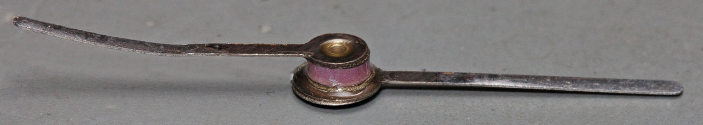
Let´s take a look into a tunnel diode! Here we have a Russian АИ201Г (AI201G) based on GaAs.
The group AI201 is used for RF oscillators. AI101 is used for amplifiers and AI301 are used for fast switching.
There are also GI30x diodes built with Ge. The GI308 is a special variant with a MESA structure.
There is also a military version: 3I201G
The last letter is used for binning the diodes. A has a very low capacitance of 8pF max Л will burden your circuit with up to 50pF.
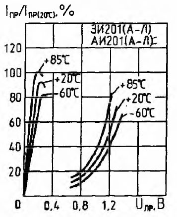
In the datasheet there is an U/I graph showing the typical tunnel diode behaviour.
The pn junction has a very high doping concentration. Due to this high doping at very low voltages electrons are tunneling through the junction leading to a fast rise of current (left part).
At higher voltages the electric field stops this tunneling before the normal diode current occurs (right part).
The two graphs are connected but due to the fast travelling from the left to the right part you often don´t see this part doing a curve trace.
The current peaks up to 16-22mA at low voltages. The ratio of the first current peak to the following low current in the valley is a quality attribute for a tunnel diode. The datasheet specifies a Ip/Iv of 10 for the IA201G.
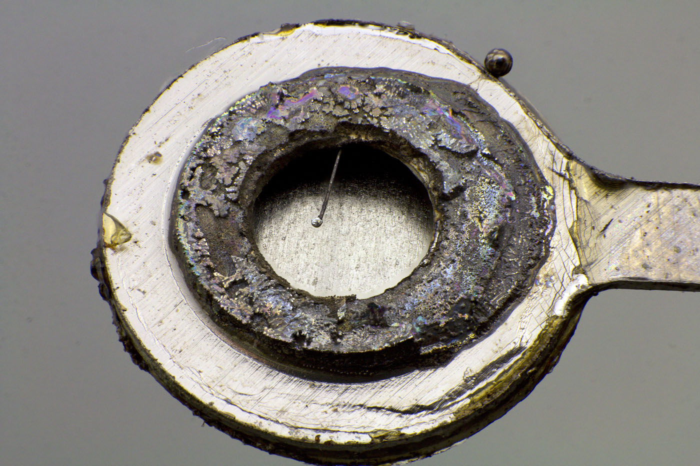
The base element of the package is a ceramic cylinder with two metal elements at the ends acting a electrical contacts. The whole part is covered with a clear coating.
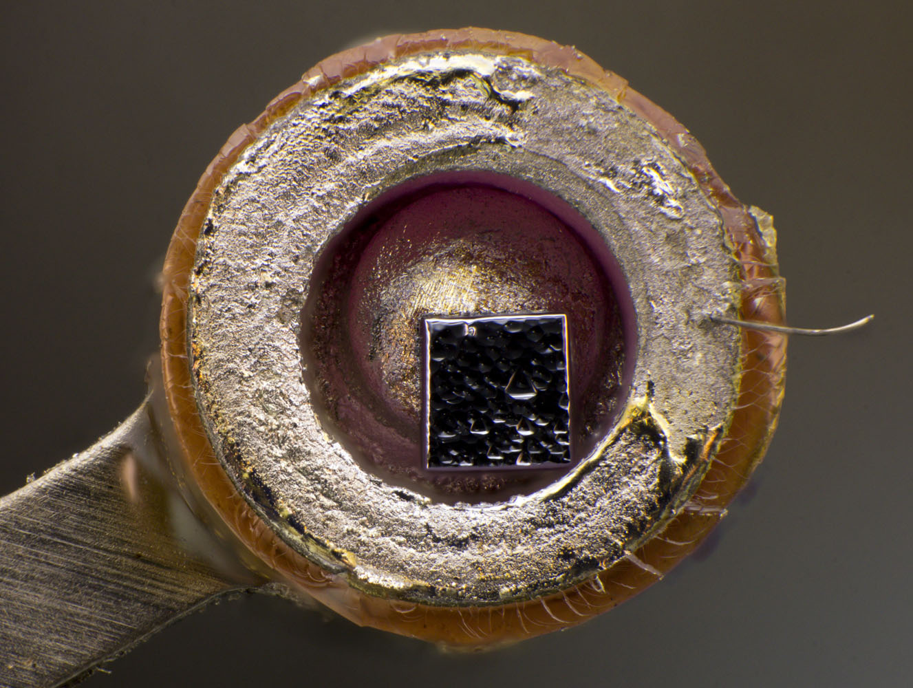
The semiconductor crystal is placed on a notch in the anode contact. In this part the crystal is placed off-center.
There is a wire connecting the crystal to the cathode which is torn off in this picture.
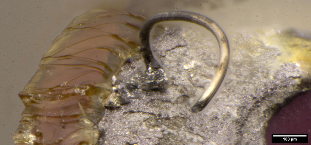
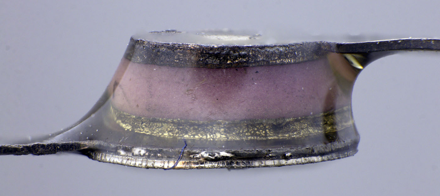
The diameter of the wire is ~30µm. The end is sharpened to reduce the contact area.
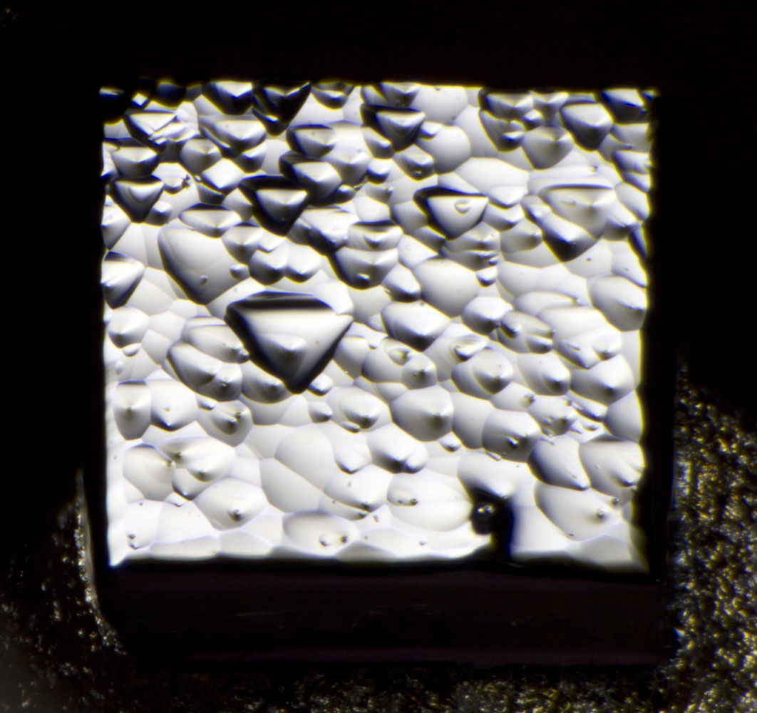
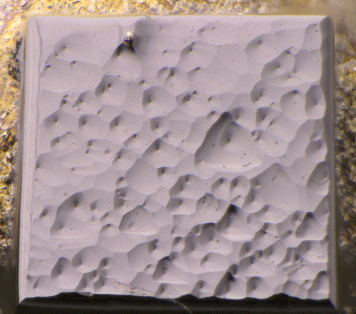
The edge length of the crystal is 0,7mm. The structure of the surface is due to etching which was done to remove impurities.
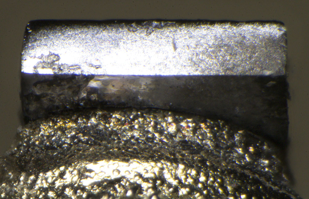
The die thickness is 0,2mm. Since it isn´t placed in the middle of the package we can take a look at the bottom of the crystal.
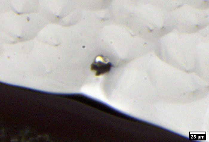
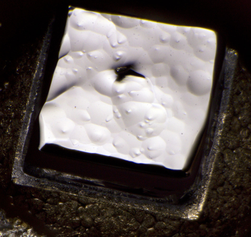
The pn junction must be highly doped in order to perform the function of a tunnel diode. For this reason, the junction cannot be constructed in the same way as for normal point-contact diodes. The high doping of a tunnel diode requires the direct alloying of an inverse doping agent, as it is done in alloy transistors. In the case of a tunnel diode, however, care must be taken to keep the alloying process short in order to produce as abrupt a pn transition as possible.
At the same time, it is important to keep the parasitic capacitance of the pn junction low. The alloy pill seen here therefore has a diameter of just 25µm. To further reduce the capacitance, one can etch down the semiconductor crystal after the alloying process to create a MESA structure. The remaining pillar is then very thin and correspondingly sensitive to mechanical and electrical stress. The GI308 mentioned above uses such a structure.
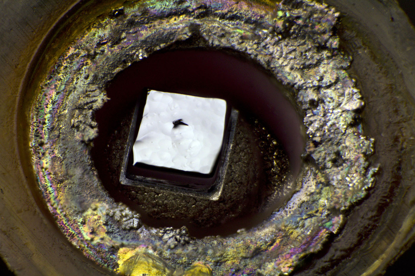
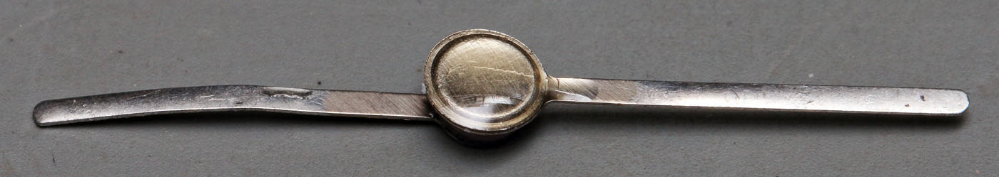
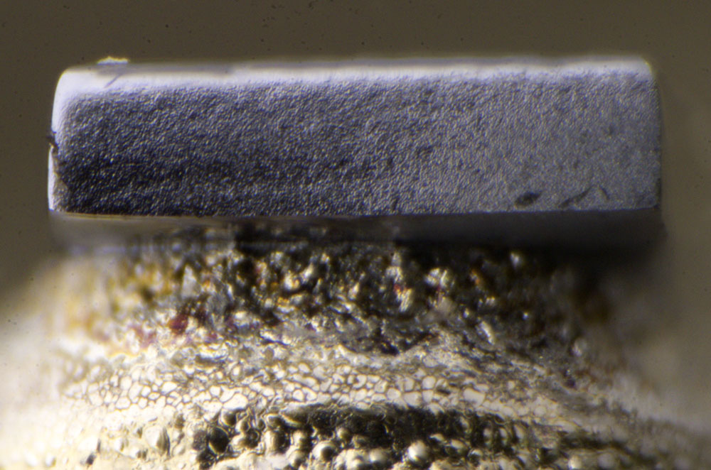
Another AI201G with a more acurate placed crystal. Here you can see how the bondwire is aranged.
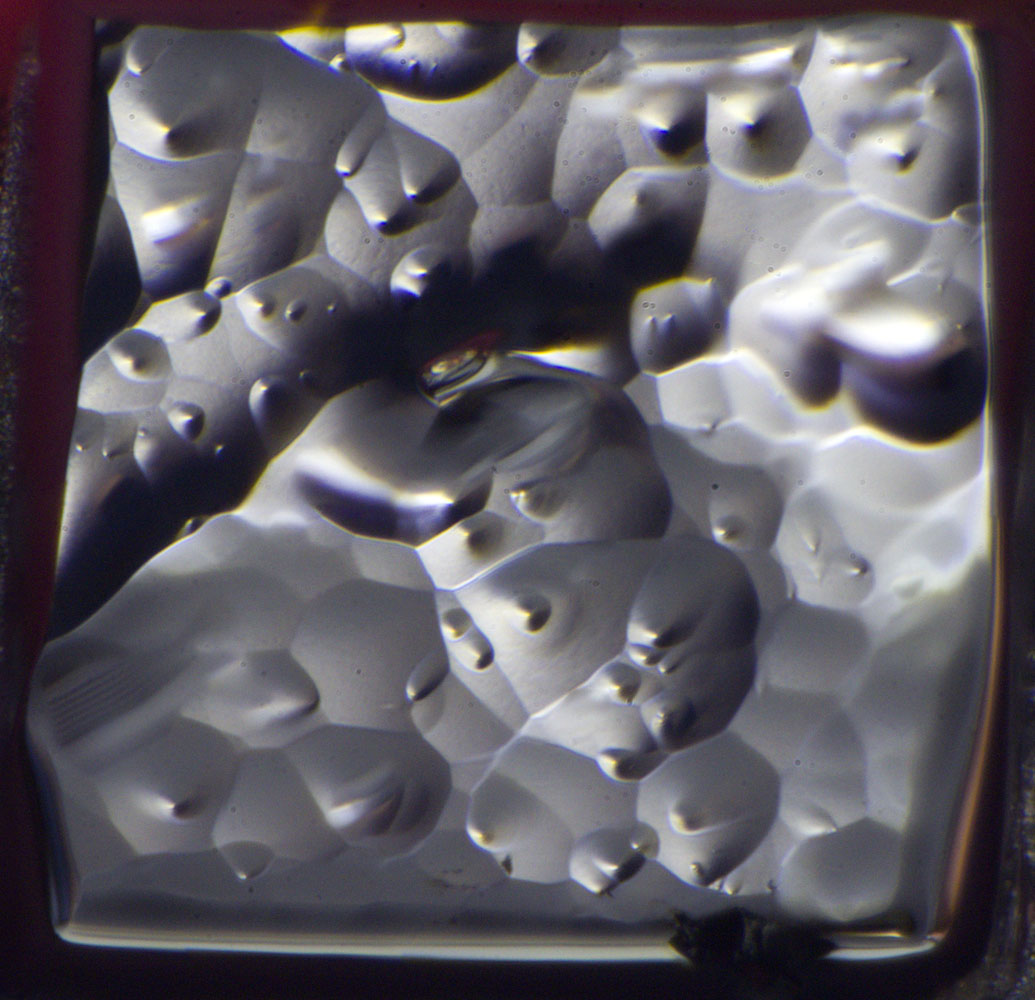
It looks like here the doping area is a little bigger (~40µm).
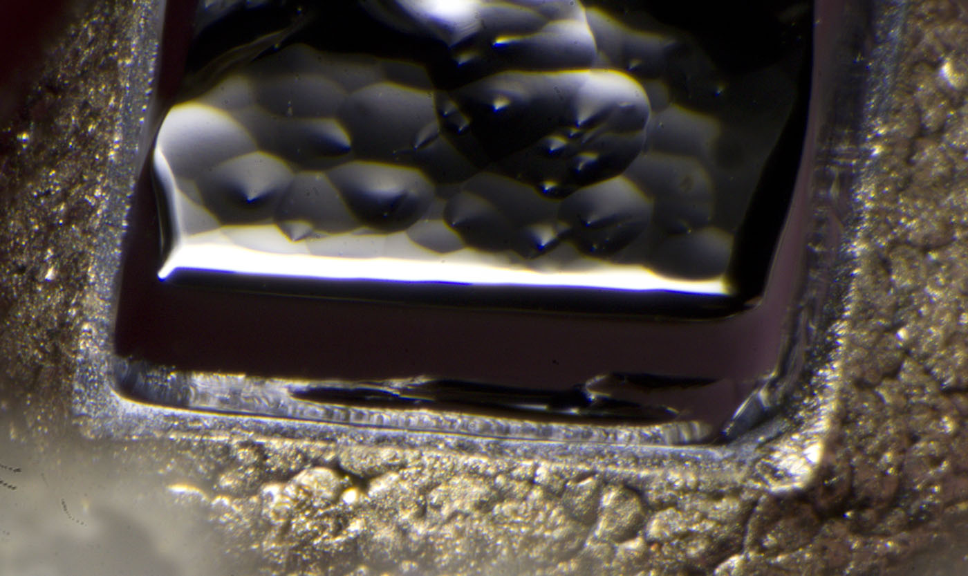
This diode is placed on some kind of a socket.
https://www.richis-lab.de/Diode07.htm 


