We had the gold wire point-contact diode OA741 (
https://www.richis-lab.de/Diode05.htm) now let´s take a look into a tungsten wire point-contact diode.
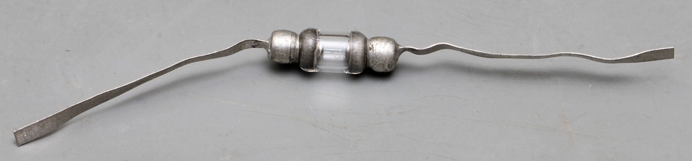
Here we have a Д2Ж (D2Ž) built in the semiconductor plant Novosibirsk. The family D2 contains seven variants, the D2Ž has the highest breakdown voltage of 150V. The leakage current is 0,25mA. The maximum mean current flow is 8mA. The maximum peak current is 25mA.
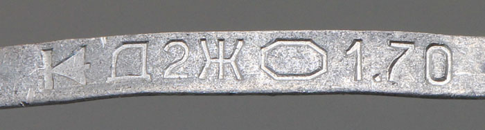
On the contact sheet there is a diode showing the current flow direction, the name Д2Ж and the logo of the semiconductor plant Novosibirsk. I don´t know what 1.70 means.
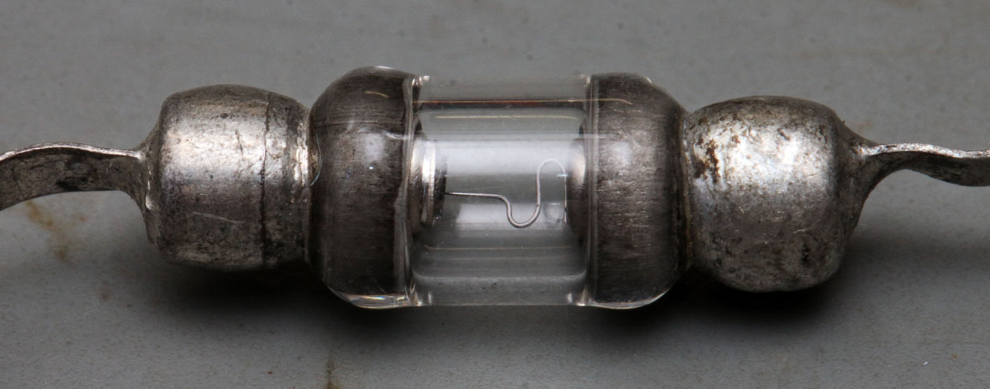
It´s a glass housing with metal caps at both ends.
The wire colour shows that it isn´t gold but probably tungsten. Sometimes the tungsten contains some dopant like aluminium.
For proper pictures a higher glass uniformity would be nice.

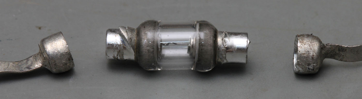

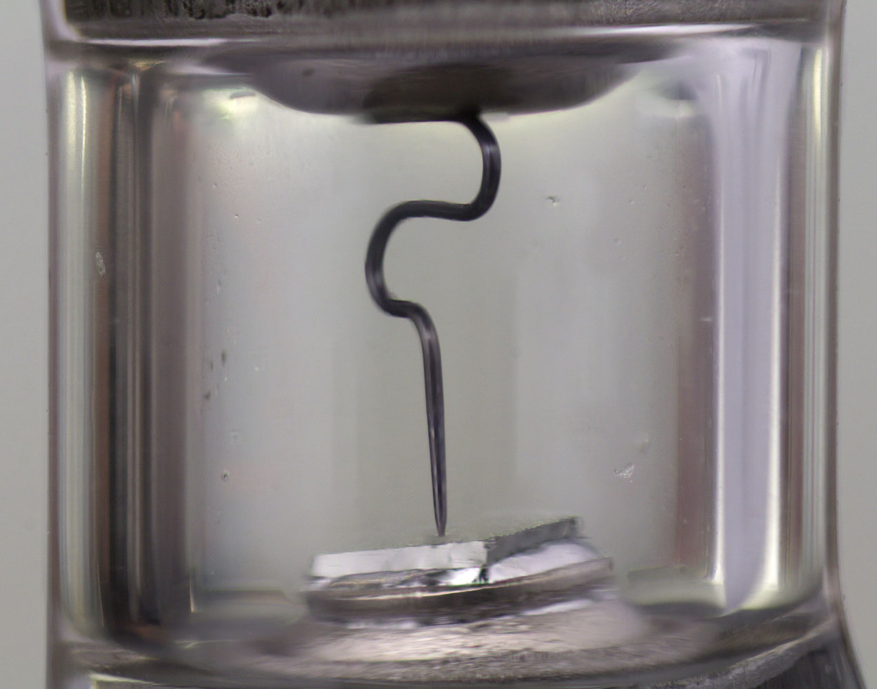
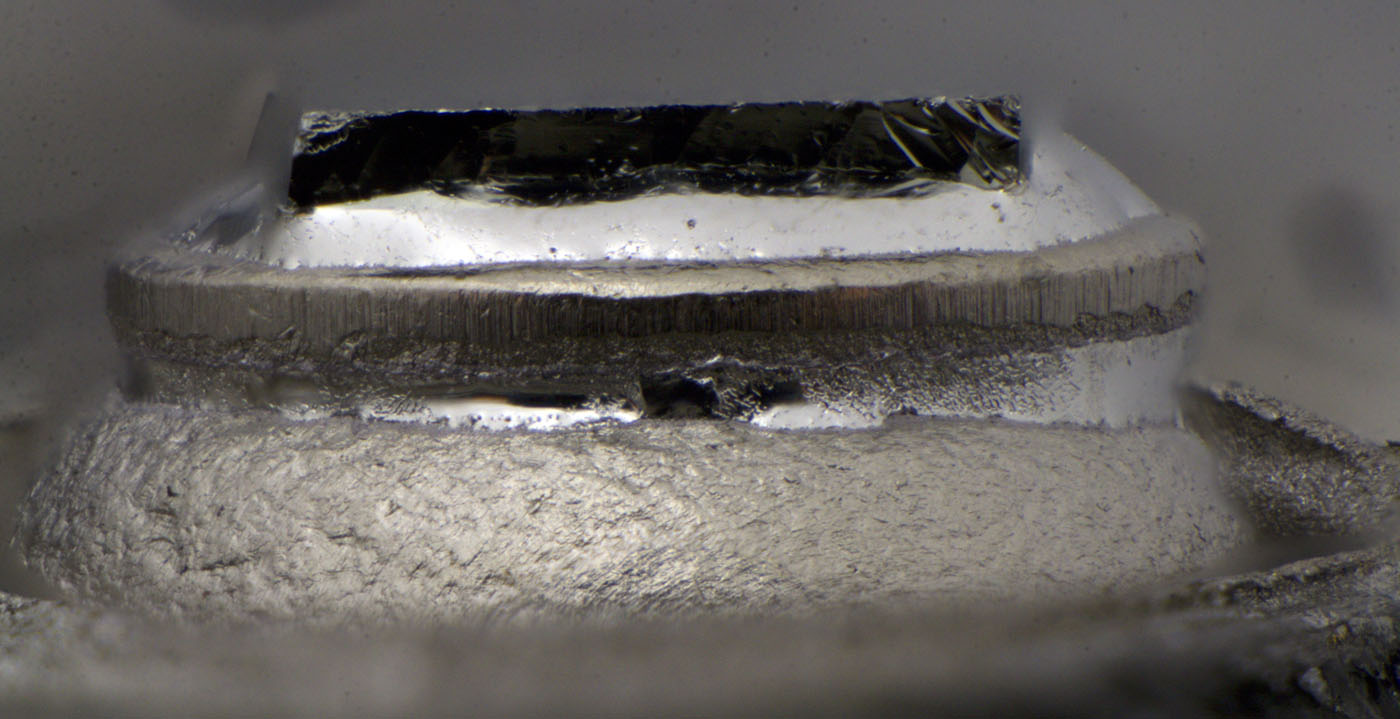
You can remove the caps at the ends. Under the caps there are shells in which they pushed cylinders carrying the germanium die and the point contact wire.
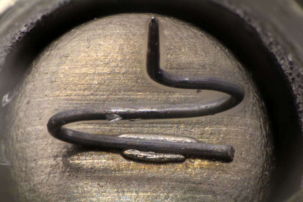
The geometry of the wire guarantees a spring effect pushing the wire onto the die and compensating different thermal expansion.
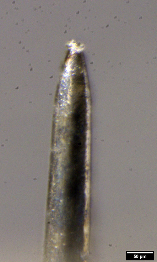
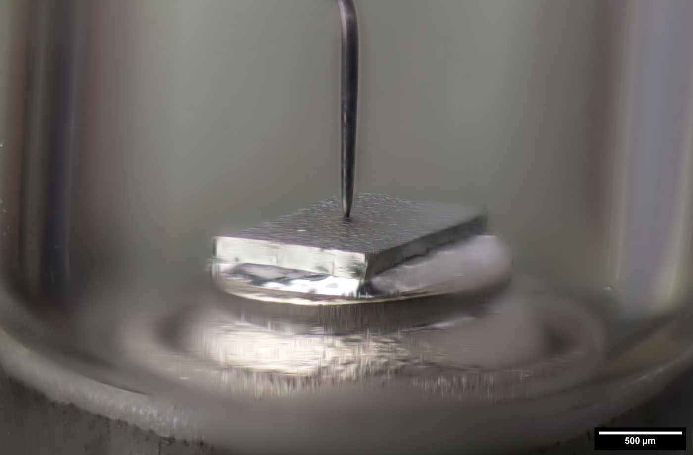
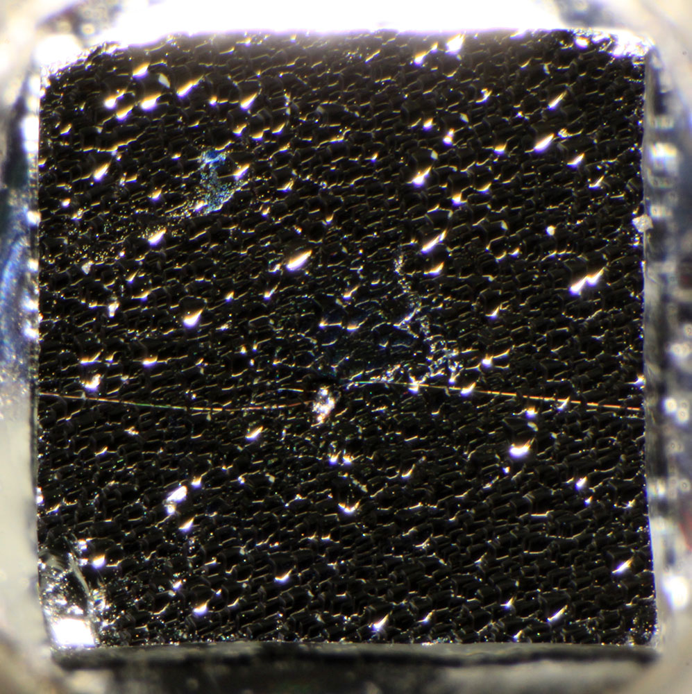
The tip of the wire is round about 30µm in diameter.

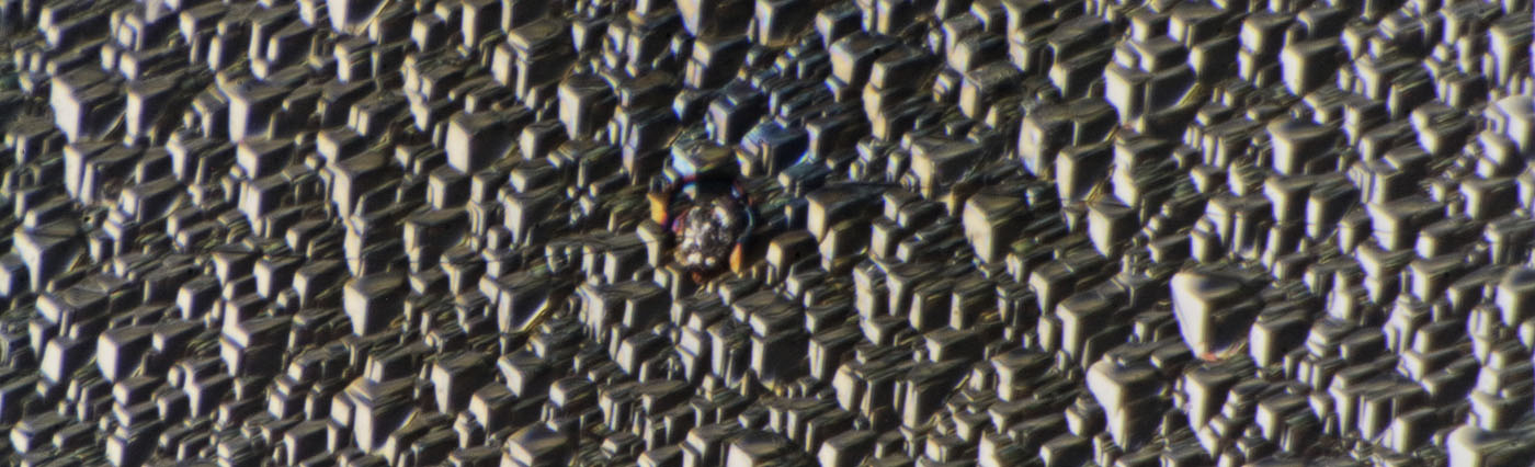
The edge length of the die is 1,2mm. The structure on the surface is formed while the impurities are etched away.
The wire was fused to the die. You can clearly see the molten germanium and the discoloration due to the heat generated in this process.
The die is at least 200µm thick while the die in the OA741 was just 80µm thick. Perhaps that is due to the different voltage ratings (40V vs. 150V).
The die sits on a round carrier that is put on the cylinder sitting in one of the shells of the package.
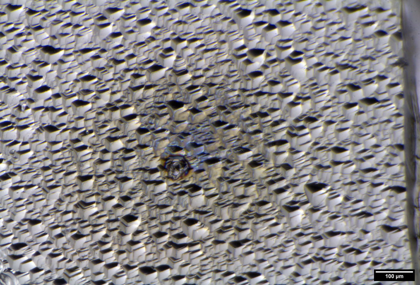
There is a crack going from one side of the die to the other. Since the diode wasn´t in use it seems like the fuse process cracked the die due to the heat exposure.
https://www.richis-lab.de/Diode06.htm 


