Author Topic: Diodes - die pictures  (Read 21383 times)

0 Members and 2 Guests are viewing this topic.

Offline mister_rf

  • Contributor
  • Posts: 33
  • Country: ro
Re: Diodes - die pictures
« Reply #50 on: January 17, 2023, 01:20:17 pm »
Old pic, old setup.
A Canon EOS 5D (the first version) camera, MP-E65 mm lens, manual rail, stacked in Helicon Focus, edited.
 

Offline mister_rf

  • Contributor
  • Posts: 33
  • Country: ro
Re: Diodes - die pictures
« Reply #51 on: January 18, 2023, 09:36:42 am »
СВЧ Д401 Point contact Germanium diode, for applications up to 10 GHz, used in old instruments as mixer and detector. Available in a ceramic case with hard leads.  Manufactured in the former Soviet Union, mid 1980s.

 
The following users thanked this post: SeanB, RoGeorge, ch_scr

Offline magic

  • Super Contributor
  • ***
  • Posts: 7067
  • Country: pl
Re: Diodes - die pictures
« Reply #52 on: January 18, 2023, 09:42:31 am »
I see that you found an image hosting site more reliable than the ImageShacks and Imgurs of the world :-DD

BTW, do you really need to embed full res versions inline? It sorta wastes everyone's (and your host's :P) bandwidth while being of little use because the images are resized anyway. With a bit more effort you could embed the auto-generated 1~2Mpx previews and make them links to the originals.
 

Offline mister_rf

  • Contributor
  • Posts: 33
  • Country: ro
Re: Diodes - die pictures
« Reply #53 on: January 18, 2023, 04:07:56 pm »
Ah, yes, the bandwidth. I think I've ignored this old dial-up era rule, mea culpa. You can see that I'm a still a rookie here, nevermind my subscription year.  ;)
As for the commons/wiki just as a simple hosting, I think there are other advantages for everyone besides free hosting.
So here we are, this time with some more work from my part.

On topic:
E220/82.5-0.005ː Selenium cartridge rectifier; Peak Reverse Voltageː 220 Volts, voltage RMS under capacitive load: 82.5 Volts, with nominal currentː 5 mA. Made in German Democratic Republic, 1950s.


The following users thanked this post: SeanB, exe, RoGeorge, BrianHG, D Straney

Offline mister_rf

  • Contributor
  • Posts: 33
  • Country: ro
Re: Diodes - die pictures
« Reply #54 on: January 19, 2023, 07:59:45 am »
D355N2000: Rectifier diode, 355 A, 2000 V; Manufactured in România, I.P.R.S. Băneasa, 1980s


The following users thanked this post: SeanB, Tjuurko, RoGeorge, D Straney

Offline NoopyTopic starter

  • Super Contributor
  • ***
  • Posts: 1867
  • Country: de
    • Richis-Lab
Re: Diodes - die pictures
« Reply #55 on: March 27, 2023, 06:55:16 pm »


The RCA CA3039 contains an array of fast diodes. The schematic above is taken from the datasheet of Intersil, where the CA3039 was still manufactured for a while. The device contains six independent diodes, with diode D6 connected to the substrate.


The integrated diodes have a very low capacitance of 0,65pF (at a reverse voltage of -2V). Reverse recovery time is typically given as 1ns (at 10mA).

The above table is from the 1978 data book "RCA Linear Integrated Circuits" and shows not only the forward voltage versus current, but also the deviation between any two diodes. Up to a current of about 1mA, the difference typically stays in the range of about 0,5mV. At higher currents, the value increases to 3mV. Specified is a maximum of 5mV at 1mA.

The very similar characteristics of the diodes are ideal for building modulators and demodulators. In general, the specifications of the device make it well suited for high frequency applications.


The potential of pin 10 is connected to the die and additionally to the housing.


The dimensions of the dies are 1.1mm x 1.0mm. The circular structure in the lower left corner is used to check the alignment of the masks against each other.

The bondpad of pin 1 is round (bottom right). In the upper area, two squares are provided where two additional bondpads could be applied. Most likely, the design has been used with other interconnections and the numbers 5516 identify the mask of the CA3039. Unlike the other bondpads, the bondpad in the lower left corner lacks the square below it. This is where the substrate is contacted.


The structures are transistors in which base and collector are short-circuited. The relatively highly doped base-emitter junction enables the fast switching times, but also leads to a low breakdown voltage of typically 7V. The datasheet even specifies just 5V as the minimum breakdown voltage.

Since the collector has a very large interface with the substrate, the parasitic capacitance with respect to the substrate is much larger (3,2pF) than the junction capacitance (0,65pF).


https://www.richis-lab.de/Diode11.htm

 :-/O
 
The following users thanked this post: SeanB, RoGeorge

Offline NoopyTopic starter

  • Super Contributor
  • ***
  • Posts: 1867
  • Country: de
    • Richis-Lab
Re: Diodes - die pictures
« Reply #56 on: August 10, 2023, 06:53:27 pm »


The OA81 is a germanium diode that was produced by several manufacturers. The optical appearance of the present diode would speak for Valvo as manufacturer, but they usually printed the company name on it. The OA81 blocks up to 75V permanently and 100V for a short time (at 75°C). The different values result from the power dissipation. At 100V and 75°C the leakage current is 450µA, which results in a power dissipation of 45mW. In the thermally well insulating glass housing, 45mW can already cause a considerable temperature rise and consequently lead to destruction of the diode.

At a current of 100µA, the forward voltage is typically 0.2V, but it rises rapidly with current and is already 2,45V typ at 30mA. The maximum is 3,3V.

The maximum permissible peak current is 150mA. In addition, a short-term overload operation with 500mA is allowed. Continuously 50mA are allowed at room temperature, at 75°C just 17mA. However, these values are only valid as long as no recurrent blocking voltage is applied. If a reverse voltage of 100V is applied alternately with the forward current, the current must not exceed 20mA (6.6mA at 75°C). Otherwise there is also the danger that the diode is thermally overloaded.

Operation at ambient temperatures above 75°C is generally not specified, since the germanium becomes uncontrollably conductive at these temperatures and thus the diode function is no longer given.


The black paint can be scraped off. As usual for such diodes, the construction is fused into a glass housing.


Inside the housing, the familiar structure of a point contact diode can be seen, in which a wire rests on a semiconductor crystal. The operation of such a diode and some technical backgrounds are documented with the OA741 (https://www.richis-lab.de/Diode05.htm). It is noticeable here that the tip rests relatively obliquely on the semiconductor.


Besides gold, tungsten was usually used as a material for the wire. Since this is obviously not gold, tungsten was probably used in the OA81.

The tungsten wire was apparently welded to the contact wire of the diode. The high temperatures have produced a number of tarnish colors.


The wire is 60µm thick. The end is usually chemically sharpened. After forming, the tip is melted into the germanium crystal to some extent, which can be seen here from the partially shiny surface.


The second wire of the diode forms a plate in the housing on which the germanium crystal is soldered. The germanium crystal has an edge length of 1,1mm and is 0,2mm thick. The regularly structured surface results from the etching process, which removes impurities on the surface.


Apparently, only the fourth placement attempt of the wire was successful. Four contact points can clearly be seen on the surface. Judging from the previous placement of the wire, one of the two contacts in the lower right corner was ultimately successful. For the other two contacts, the wire does not appear to have fused with the semiconductor.


https://www.richis-lab.de/Diode12.htm

 :-/O
 
The following users thanked this post: SeanB, RoGeorge, ch_scr

Online exe

  • Supporter
  • ****
  • Posts: 2607
  • Country: nl
  • self-educated hobbyist
Re: Diodes - die pictures
« Reply #57 on: August 10, 2023, 08:18:36 pm »
Wow, didn't know germanium diodes were so finicky. Forward voltage of 3.3V@30mA sounds ridiculous by modern standards. It also rises rapidly with current. Doesn't look like a typical pn-junction. Can it be due to the point contact? I mean, it only conducts in small area/volume of the die, or not?
 

Offline T3sl4co1l

  • Super Contributor
  • ***
  • Posts: 22288
  • Country: us
  • Expert, Analog Electronics, PCB Layout, EMC
    • Seven Transistor Labs
Re: Diodes - die pictures
« Reply #58 on: August 10, 2023, 08:37:56 pm »
Yes, point contact; the resistance is all in that tiny little spot.  So it works well for small signals, but a 6AL5 for example outperforms it at... um, certain currents I think? Not actually high currents, and not very much at low currents given the low drop.  6AL5 outperforms most silicon diodes at low currents though (of course, if you wholly ignore the heater power cost :) ).

Given the trouble of heaters, and generally high plate voltages outside of diodes, it's no accident tubes went away.

Tim
Seven Transistor Labs, LLC
Electronic design, from concept to prototype.
Bringing a project to life?  Send me a message!
 

Offline NoopyTopic starter

  • Super Contributor
  • ***
  • Posts: 1867
  • Country: de
    • Richis-Lab
Re: Diodes - die pictures
« Reply #59 on: August 11, 2023, 11:12:08 am »
Wow, didn't know germanium diodes were so finicky. Forward voltage of 3.3V@30mA sounds ridiculous by modern standards. It also rises rapidly with current. Doesn't look like a typical pn-junction. Can it be due to the point contact? I mean, it only conducts in small area/volume of the die, or not?

It is a pn-junction but probably one wouldn´t call it typical.  ;D

A point contact in the first place is kind of a Schottky diode.
The high current that melts the contact area generates a pn-junction. In the molten semicondcutor material negative charge carriers are traveling deeper into the semicondcutor and positive charge carriers are accumulating at the surface.
Sometimes the point contact wires were doped a little to add some p dopant.

 
The following users thanked this post: SeanB, RoGeorge

Offline NoopyTopic starter

  • Super Contributor
  • ***
  • Posts: 1867
  • Country: de
    • Richis-Lab
Re: Diodes - die pictures
« Reply #60 on: December 14, 2023, 07:36:41 pm »


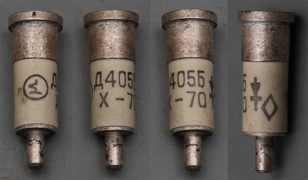
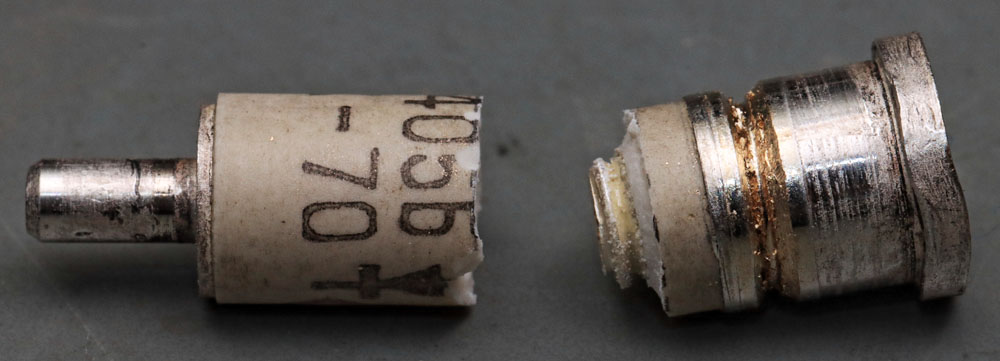
The Д405Б (D405B) is a microwave diode in a cartridge housing. It is a point contact diode. According to the datasheet, it is designed for operation in the wavelength range around 3 cm, which corresponds to a frequency of 10 GHz. The printed logo is reminiscent of the contact wire of a point contact diode and belongs to the Russian factory for semiconductor components Tomilinsky.


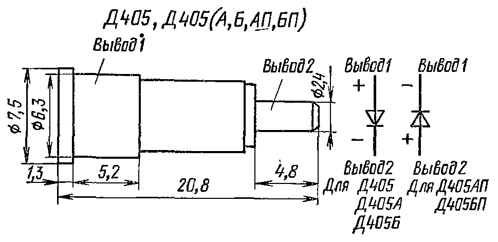
The D405 is available with different polarities. In the variant with the additional index П (P), the anode potential is applied to the thinner contact. In the variant without П, the anode potential is applied to the contact with the larger diameter.


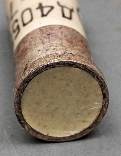
The larger contact is filled with a light-colored potting compound. There is often a screw there, which is also the case here. However, the screw cannot be moved after it has been exposed. The screw was probably glued in, as the housing must be as tight as possible to ensure a long service life.


When I tried to cut off the lower element, the housing broke. Here you can see how far the thread of the lower part protrudes into the ceramic cylinder.


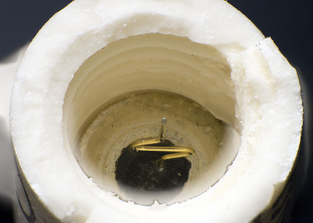
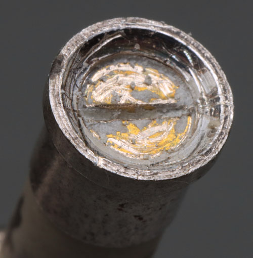
The part with the thinner connection contains the contact wire of the diode.


The thread runs completely through the ceramic cylinder.

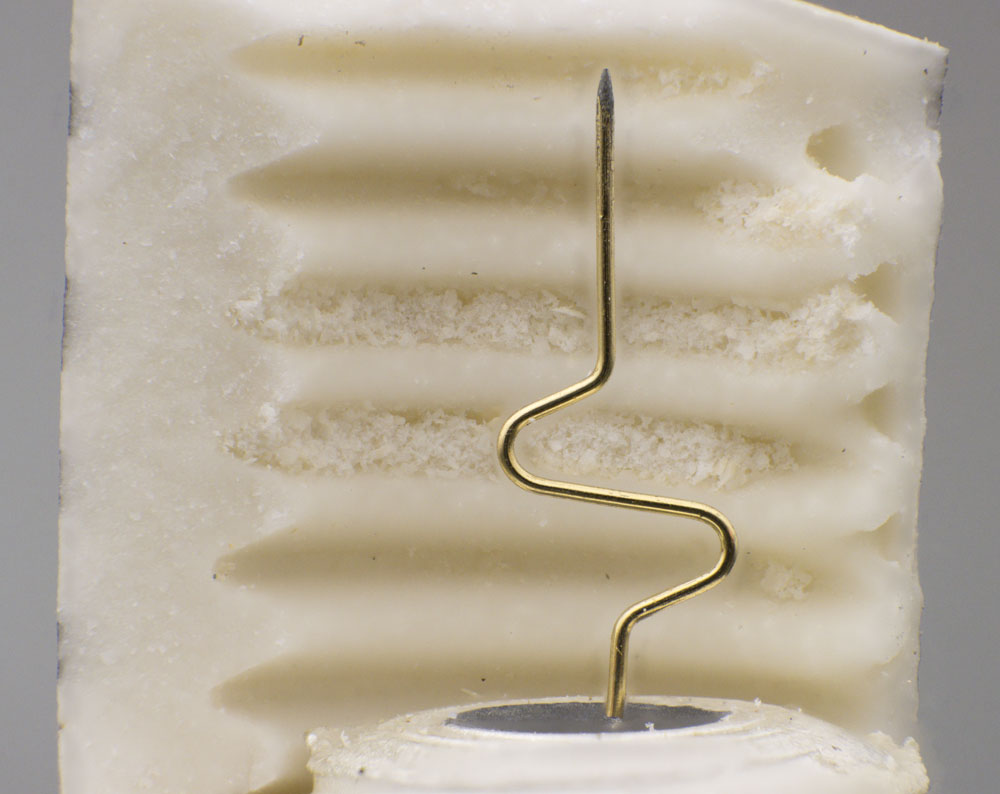
The geometry of the wire provides a certain elasticity, which ensures good contact and at the same time limits the contact pressure to a certain extent.


The wire disappears into a black mass, which probably serves as mechanical stabilization.


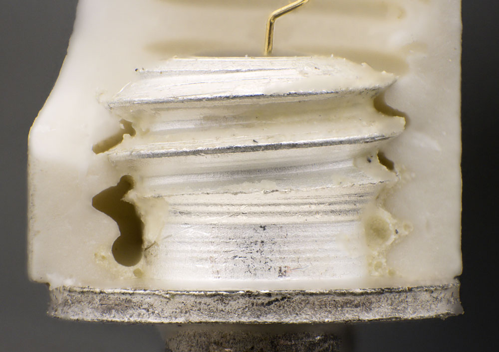
The contact elements are screwed into the ceramic cylinder as far as they will go. The screw in the larger contact can then be used to move the wire and the semiconductor crystal towards each other until the desired contact pressure is achieved. A light-colored material can be seen between the ceramic body and the thread of the contact, which fixes the thread and seals the inside.


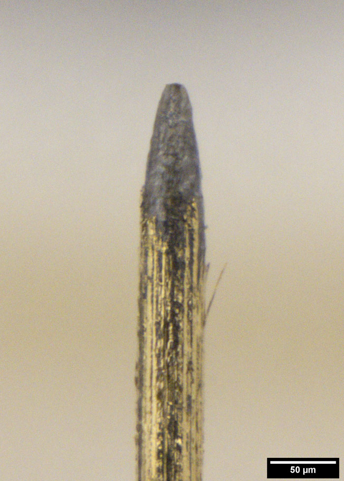
The wire has a diameter of approximately 50µm. At the tip, the diameter is approximately 15µm. The so-called diode bible (Halbleiterdioden - Leitfaden für Erwachsenen-Qualifizierung und Ausbildung im VEB Werk für Fernsehelektronik by Heinz Hornung) states that tungsten or molybdenum or alloys of the two materials are usually used for such high-frequency diodes. The surface was obviously coated with gold. The diode bible further describes that the tips often just have a diameter of 8µm.


Ordinary tip diodes are formed. This involves a relatively high current flowing through the tip contact, which heats up the contact area locally and thus melts it. During this formation, a pn junction is formed and the contact area is mechanically stabilized. More extensive melting produces a higher dielectric strength, which is desirable for conventional diodes such as the OA741 (https://www.richis-lab.de/Diode05.htm). At the same time, however, the junction capacitance increases. If the diode is to be used at very high frequencies, this is a major disadvantage. The diode bible explains that high-frequency diodes based on gallium arsenide are still formed. High-frequency diodes based on silicon, on the other hand, are usually not formed. The simple contact already provides a sufficient rectification effect. The physical effects that occur at the contact surface are described in more detail with the OA741.

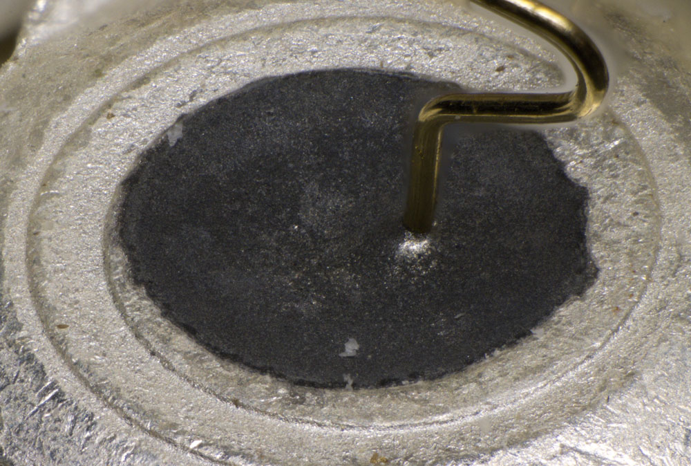
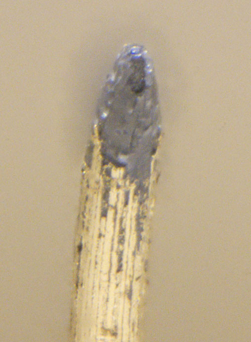
The optical appearance of the wire tip also indicates that no forming took place here. No remnants of a broken connection can be seen. The surface is slightly darker directly at the tip and slightly to the side, but this could have been caused during processing or by the operating current.


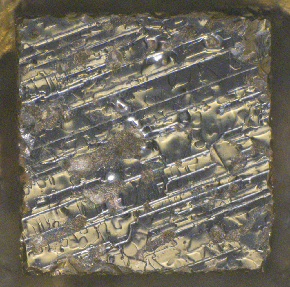
The silicon crystal inside the thicker contact has an edge length of 1 mm.


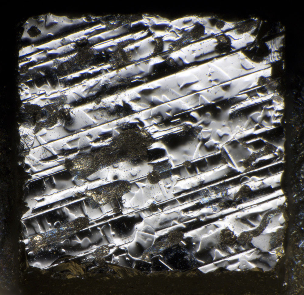
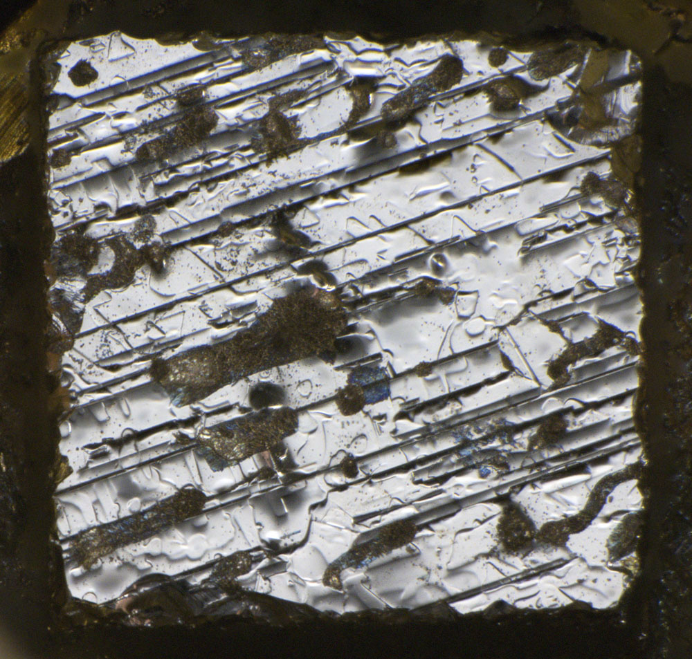
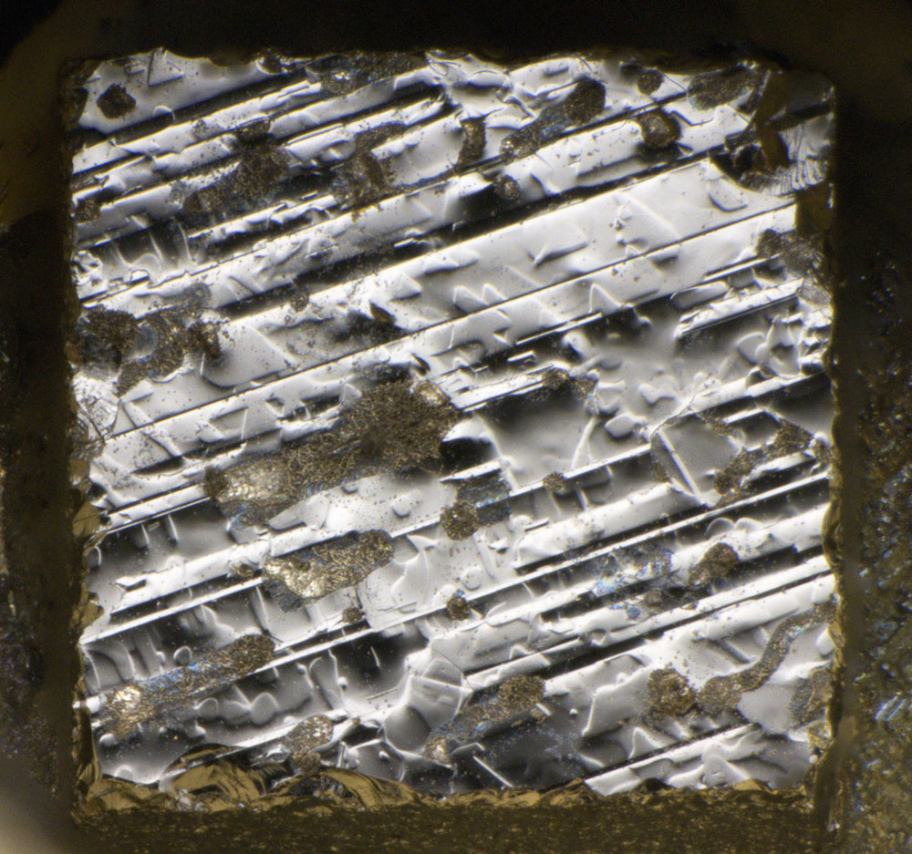
The crystal shows an interesting surface. Different exposures can be used to bring out different characteristics. Dirt has accumulated on the surface. According to the optical appearance, it could be solder.

A contact point with the wire tip is not visible. This also indicates that the diode was not formed.


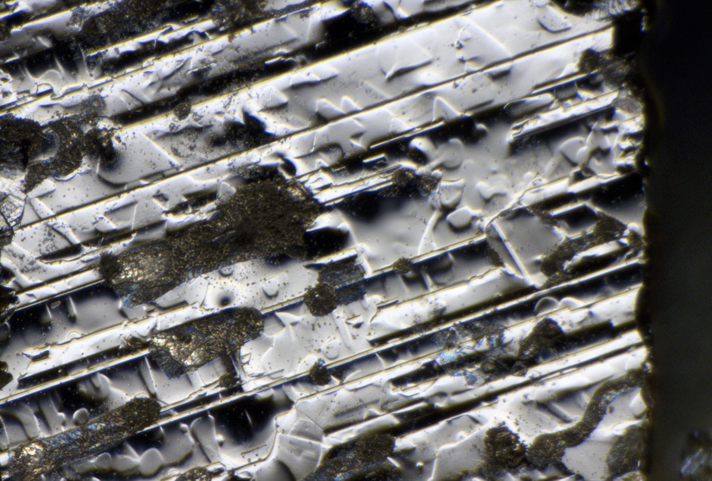
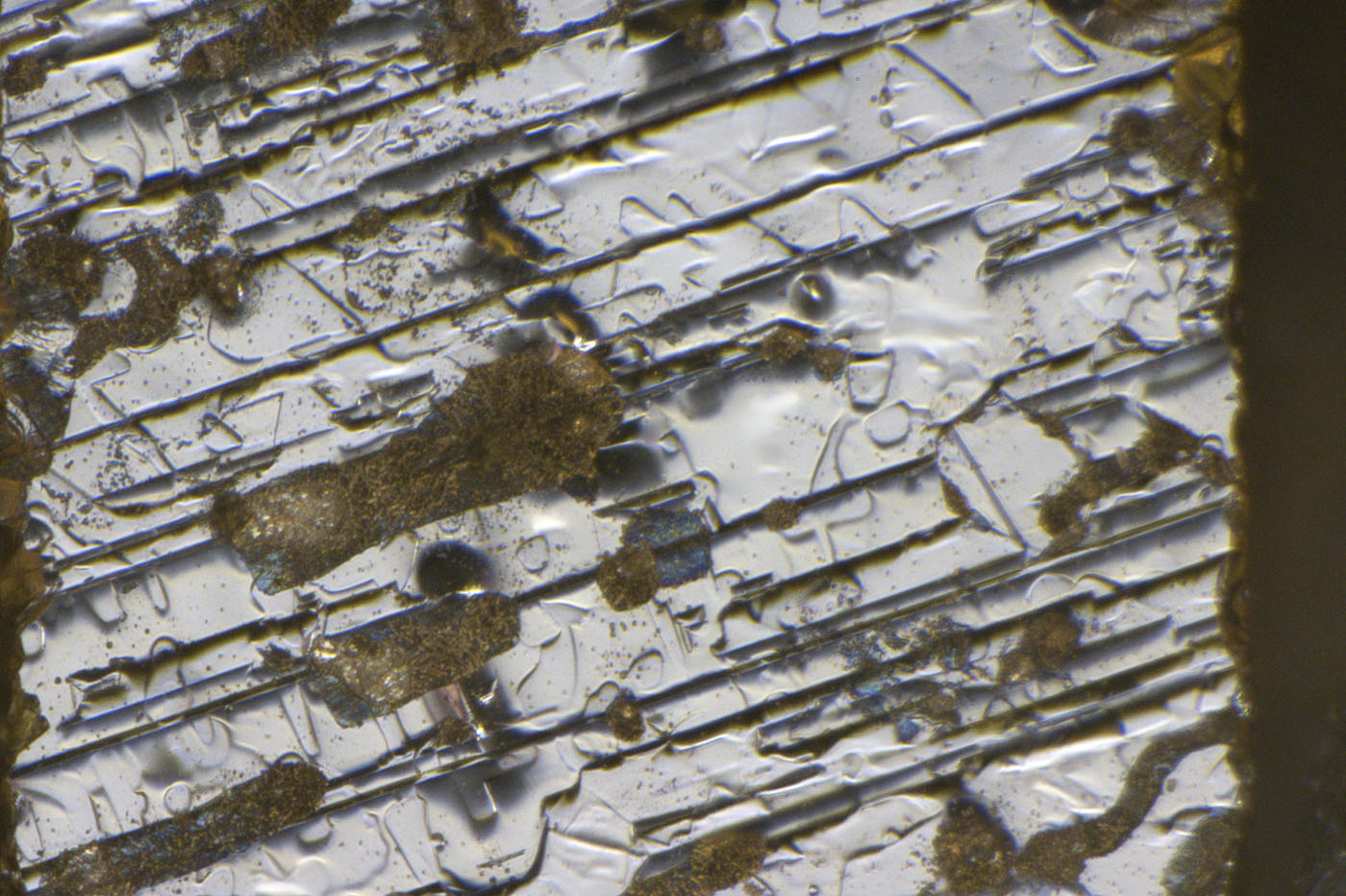
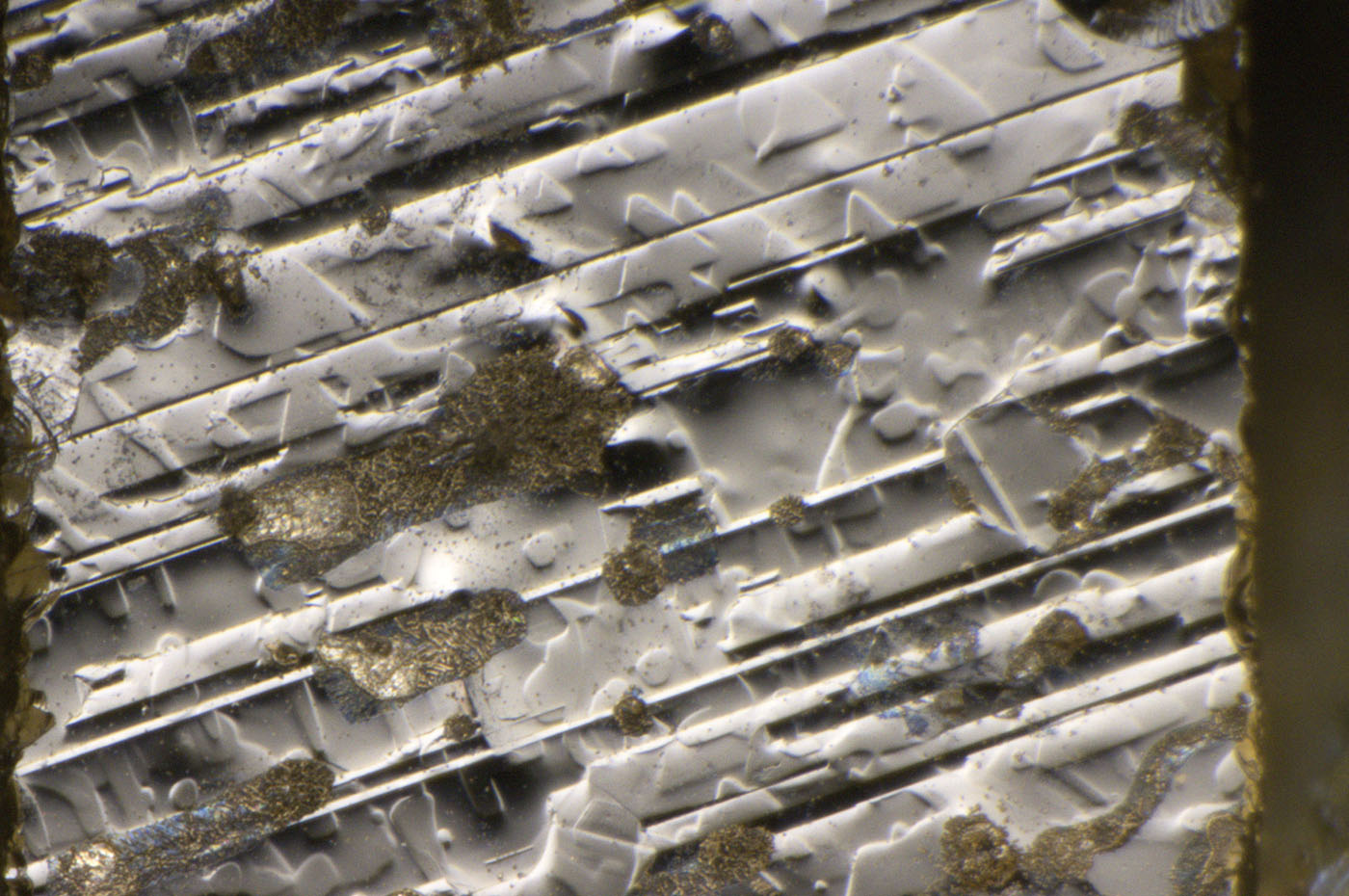
Apart from the "dirt", two different structures are visible on the crystal surface. There are furrows from the top right to the bottom left, as would be expected after mechanical processing. In addition, there are structures that often occur during etching processes. However, these structures are rather irregular here.


https://www.richis-lab.de/Diode13.htm

 :-/O
 
The following users thanked this post: SeanB, RoGeorge, Miyuki, ch_scr, D Straney, mawyatt

Offline Miyuki

  • Frequent Contributor
  • **
  • Posts: 907
  • Country: cz
    • Me on youtube
Re: Diodes - die pictures
« Reply #61 on: December 15, 2023, 09:51:02 am »
That chip looks like covered with some hieroglyphs
Maybe it is the way they put the magic smoke in
 

Offline NoopyTopic starter

  • Super Contributor
  • ***
  • Posts: 1867
  • Country: de
    • Richis-Lab
Re: Diodes - die pictures
« Reply #62 on: December 15, 2023, 10:16:20 am »
Some magic incantations?  ;D

Offline RoGeorge

  • Super Contributor
  • ***
  • Posts: 6636
  • Country: ro
Re: Diodes - die pictures
« Reply #63 on: December 15, 2023, 10:52:10 am »
That chip looks like covered with some hieroglyphs

Looks like hieroglyphs from an alien spaceship.  8)

Online iMo

  • Super Contributor
  • ***
  • Posts: 5071
  • Country: bt
Re: Diodes - die pictures
« Reply #64 on: December 15, 2023, 11:04:33 am »
The crystals were made of the rare material found in the Podkamennaya Tunguska River..
 

Offline David Hess

  • Super Contributor
  • ***
  • Posts: 17065
  • Country: us
  • DavidH
Re: Diodes - die pictures
« Reply #65 on: December 15, 2023, 03:12:00 pm »
That chip looks like covered with some hieroglyphs

Looks like hieroglyphs from an alien spaceship.  8)

Goa'uld technology.
 

Offline NoopyTopic starter

  • Super Contributor
  • ***
  • Posts: 1867
  • Country: de
    • Richis-Lab
Re: Diodes - die pictures
« Reply #66 on: January 23, 2024, 05:13:12 am »


The ГИ308Б (GI308B) is a germanium-based tunnel diode. The G stands for germanium. The following two characters show the applications for which the diode is optimised. I3 stands for switching applications. The datasheet mentions switching devices in the sub-nanosecond range. The variant specified for military applications has a 1 in the first position of the designation: 1И308Б.

The datasheet already reveals that it is a MESA diode. The index refers to one of nine bins with different capacitances and peak voltages. Diodes with the index B offer a capacitance of 0,7pF to 2pF and a peak voltage of 70mV to 110mV. Whilst the AI201G still had connection terminals, the GI308B makes direct contact with the small housing. This reduces the inductance, which is helpful for high-frequency applications. The diameter of the housing is just 3,6mm and the height is specified with 1,6mm.


The individual tunnel diodes are shrink-wrapped in plastic film with small pieces of paper.


On the label you can see that it originally read ГИ308Г (GI308G), which has been corrected to ГИ308Б (GI308B). The symbol reminiscent of an X and the three characters on the far right cannot be assigned.

The company to which the logo belongs has a long history and has been renamed several times during this time. At the time of manufacture, it was probably Moscow plant no. 311. The company still exists today and is called Optron.


Coloured dots indicate the different bins. The green dot in combination with a black and a white dot stands for the GI308B.


The housing is based on a ceramic cylinder. The ends of the cylinder are closed with metal plates. The wider element consists of two parts soldered together. It can be assumed that during production the diode was inserted into the housing through the wider element.


The wider contact of the tunnel diode is smooth.


I wasn´t able to open the solder joint, but both metal elements eventually detached from the ceramic body. This revealed that the semiconductor was connected to the contact of the housing via a thin metal grid. The wide metal grid and the connection via two sides ensures a low parasitic inductance, which is necessary to achieve short switching times and high frequencies. The datasheet specifies 0,2nH to 0,35nH.


The die has an edge length of 0,36 mm. The small, not quite centred element is the actual diode. The metal grid contacts this element. It also rests on the edges, which increases the mechanical stability. The edges must therefore be insulating.


The metal grid is soldered onto the diode. The diode structure is mechanically and thermally very sensitive. Accordingly, a low-melting solder had to be used here.

In the picture below you can already see that the diode structure consists of a larger element that tapers towards the substrate.


The so-called diode bible explains what can be seen here (Halbleiterdioden - Leitfaden für Erwachsenen-Qualifizierung und Ausbildung im VEB Werk für Fernsehelektronik by Heinz Hornung). In the manufacture of such a tunnel diode, a very small bead of a metal mixture is first applied to a germanium crystal and alloyed with it. The diode bible speaks of a tin-antimony-arsenic mixture. Tin is the carrier material, arsenic is the dopant and arsenic improves wetting. After alloying, the germanium crystal is selectively electrolytically removed. The result is a mushroom shape with a very small pn junction and a correspondingly small junction capacitance.

In addition to the small active area, very high doping with an abrupt pn junction is also necessary to achieve the desired tunnelling diode effect. The very high doping and the small active area are the reason why such tunnel diodes can be damaged even at low currents. For this reason, tunnelling diodes must not be measured with a diode tester, for example. Another weak point is the mechanical stability. The diode bible describes that the construction is therefore moulded with a lacquer. This was apparently not necessary with the GI308B.


While removing the grid the mushroom head also breaks off and the base of the construct becomes visible. The mushroom head had a diameter of about 60µm. The diameter of the base at the upper end is just about 10µm.


https://www.richis-lab.de/Diode14.htm

 :-/O
 
The following users thanked this post: SeanB, doktor pyta, RoGeorge, ch_scr, D Straney

Online exe

  • Supporter
  • ****
  • Posts: 2607
  • Country: nl
  • self-educated hobbyist
Re: Diodes - die pictures
« Reply #67 on: January 23, 2024, 08:47:03 am »
The symbol reminiscent of an X and the three characters on the far right cannot be assigned.

"91Г" looks like abbreviation of "1991 Год", or year of production.

As of "X", I don't really know, I think it may mean "trust the correction" ("исправленному верить"), or it's a signature of the person who did the packaging, but I don't have any evidence to support that. So, pure speculation)
 
The following users thanked this post: Noopy

Offline NoopyTopic starter

  • Super Contributor
  • ***
  • Posts: 1867
  • Country: de
    • Richis-Lab
Re: Diodes - die pictures
« Reply #68 on: January 23, 2024, 07:34:26 pm »
Thank you for your explanation exe!  :-+

I got the same explanation from another supporter. He also told me that on old typwriters there was no 1 and so one often used the I instead. It seems I´m to young to know this...  ;D

Offline NoopyTopic starter

  • Super Contributor
  • ***
  • Posts: 1867
  • Country: de
    • Richis-Lab
Re: Diodes - die pictures
« Reply #69 on: May 11, 2024, 03:50:08 am »


The SKiiP 81 AN 15 T10 module is a three-phase bridge rectifier built by Semikron. The datecode is made up of two numbers for the year and two numbers for the calendar week. The last number stands for the production batch of that week. The module was therefore produced in calendar week 7 of 2004.


The package type is called MiniSKiiP. Variant 8a was used here. However, the illustration does not quite match the module in question. The SKiiP 81 AN 15 T10 only contains the bridge rectifier and the temperature sensor. The chopper path is not fitted.


The two images above show the basic structure of the MiniSKiiP modules and how they can be integrated into an application. The picture on the left is from Semikron. The picture on the right is from Vincotech, a subsidiary of Mitsubishi Electric Corporation, which also uses the MiniSKiiP modules.

The module is based on a ceramic carrier on which the semiconductors are located. The potentials of the circuit are routed upwards through the package using spring contacts. The thinner spring contacts of the smaller module types can be seen here. The package variant 8 has larger, barrel-shaped contacts. A circuit board is then placed on the top. Two screws generate the necessary contact pressure, which is distributed over the entire surface by a plastic element.


This overview gives a feeling for the module variants that Semikron had on offer and how the designations are made up. Module variant 8 allows currents of up to 130A, while the smaller module variants do not allow more than 75A.

The datasheet for the SKiiP 81 AN 15 T10 specifies a dielectric strength of 1.500V and a current carrying capacity of 100A (at 85°C) for the diodes, whereby the current is limited by the spring contacts. Up to 1.000A are permissible for short periods.


On the underside of the module the ceramic substrate is coated with a copper layer. The datasheet specifies a maximum thermal resistance of 1K/W for each diode.


The gel potting was probably inserted through the two holes in the upper area after assembly. The package shows some options. The three high-current contacts and the control contact of the chopper can be inserted on the right. On the left, there is the option of controlling thyristors with six control contacts.


The plastic housing can be lifted off the ceramic carrier relatively easily.


The high-current contacts have angled, spring-loaded metal strips on both sides. The contacts are a little longer than plastic housing so that a certain amount of contact pressure is created during assembly.


The cylindrical high-current contacts are open on one side. The package has wedge-shaped elements that retract into these gaps. The small contacts consist of just one piece of wire that has been bent several times to create a certain spring effect.


The ceramic plate is 1 mm thick. Where the gel potting is not evenly flat, it disturbs the view, but the functions can still be easily recognised.


The diodes of the rectifier bridge are represented by individual semiconductors. The PTC, which can be used to determine the temperature of the module, is located in the top right-hand corner. The chopper is obviously constructed with two transistors. In addition to the freewheeling diode Dbr, there is also a diode Dt in parallel with the transistors.


The edge length of the diodes is 7mm. Seven bondwires contact the diodes.


The diodes appear to have a MESA structure, a black coating protects this area.


The shiny surface of the temperature sensor suggests that it is a diode. However, measurements show that it is actually a PTC resistor.


https://www.richis-lab.de/Diode15.htm

 :-/O
 
The following users thanked this post: macboy, RoGeorge


Share me

Digg  Facebook  SlashDot  Delicious  Technorati  Twitter  Google  Yahoo
Smf