Author Topic: Diodes - die pictures  (Read 21382 times)

0 Members and 2 Guests are viewing this topic.

Offline T3sl4co1l

  • Super Contributor
  • ***
  • Posts: 22288
  • Country: us
  • Expert, Analog Electronics, PCB Layout, EMC
    • Seven Transistor Labs
Re: Diodes - die pictures
« Reply #25 on: February 18, 2022, 01:38:52 pm »
Think it would make sense to do it at higher signal level, or lower impedance.  It's hard to tell recovery from capacitance at this scale; indeed you often see signal schottky diodes with "recovery" ratings, but it's basically just capacitance in the fixture (similar signal levels and resistance as this).

The spike is relative to the previous baseline, as that's what the junction capacitance was charged to; so it can apparently overshoot the input by about Vf.  Indeed, the 1N4004 generates voltage once charged, acting something like a microscopic battery -- exponential charge(Vf) curve included.  Once its stored charge is released (or decays -- it's also a very leaky battery, t ~ 10us), voltage is free to swing to zero or reverse.  (Its recovery can be modeled as a nonlinear capacitance, and indeed this is how SPICE does it.)  The long "drool" tail is where recovery losses are dissipated -- some current continues to flow but the junction voltage is already reversed, thus dissipating quite large peak power, hence why these are unsuitable for high frequency application.

When the device has capacitance, there is current flow in reverse, but only in relation to change in voltage (dV/dt).  This is a subtle difference compared to a merely decreasing current, so it does indeed again look like recovery.  The key is, the power spent in reverse recovery is reabsorbed on the forward swing -- capacitance is conservative.  (It's dissipated in this circuit anyway, because the capacitance is dis/charged by the 100 ohm resistor; but if you measured the power in each component, you'd see it's absorbed by the resistor, not the diode.  We can take advantage of this with an LC circuit, as in a resonant converter, where the capacitive energy can be recycled into the next phase and so on.)  So it appears the FERD is capacitance-dominant.

Note the 1N4004 has a not-quite-flat Vf at turn-on: it settles down very slightly.  This is in part due to absorbing some extra charge -- the charge which is released during recovery.  The excess Vf is known as forward recovery, and is usually quite minor, but can be problematic for some types against fast waveforms.

Although the leads are quite long/loose, it appears risetime is modest in comparison, or the 100 ohm load is adequate damping; no inductive effects appear to be at play here.  Just capacitive coupling. :-+

Tim
Seven Transistor Labs, LLC
Electronic design, from concept to prototype.
Bringing a project to life?  Send me a message!
 
The following users thanked this post: exe

Offline NoopyTopic starter

  • Super Contributor
  • ***
  • Posts: 1867
  • Country: de
    • Richis-Lab
Re: Diodes - die pictures
« Reply #26 on: May 08, 2022, 12:27:06 pm »


Let´s take a look into a tunnel diode! Here we have a Russian АИ201Г (AI201G) based on GaAs.

The group AI201 is used for RF oscillators. AI101 is used for amplifiers and AI301 are used for fast switching.
There are also GI30x diodes built with Ge. The GI308 is a special variant with a MESA structure.

There is also a military version: 3I201G

The last letter is used for binning the diodes. A has a very low capacitance of 8pF max Л will burden your circuit with up to 50pF.
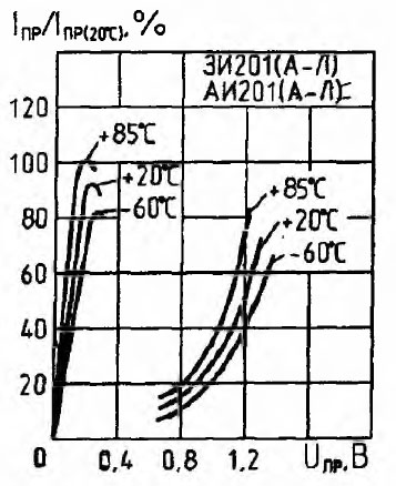


In the datasheet there is an U/I graph showing the typical tunnel diode behaviour.

The pn junction has a very high doping concentration. Due to this high doping at very low voltages electrons are tunneling through the junction leading to a fast rise of current (left part).
At higher voltages the electric field stops this tunneling before the normal diode current occurs (right part).
The two graphs are connected but due to the fast travelling from the left to the right part you often don´t see this part doing a curve trace.

The current peaks up to 16-22mA at low voltages. The ratio of the first current peak to the following low current in the valley is a quality attribute for a tunnel diode. The datasheet specifies a Ip/Iv of 10 for the IA201G.
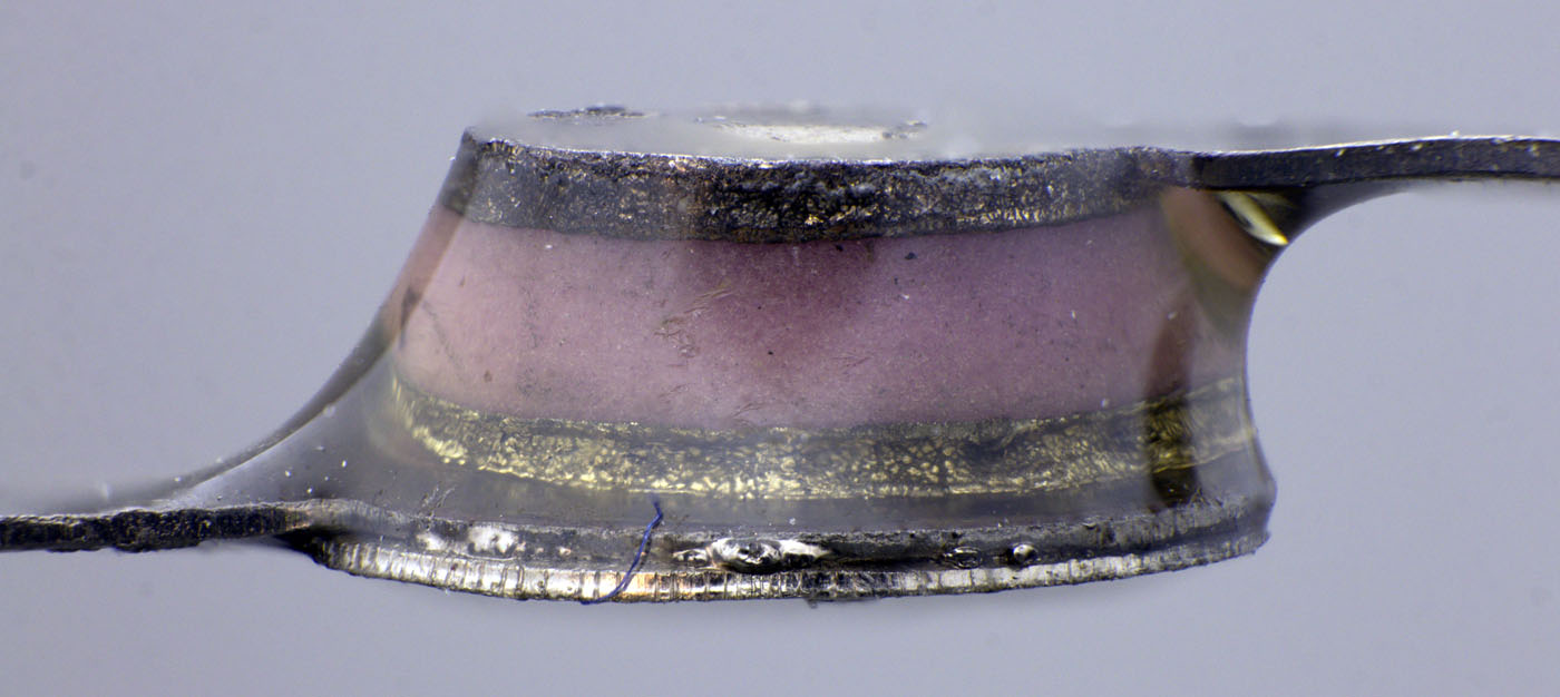


The base element of the package is a ceramic cylinder with two metal elements at the ends acting a electrical contacts. The whole part is covered with a clear coating.
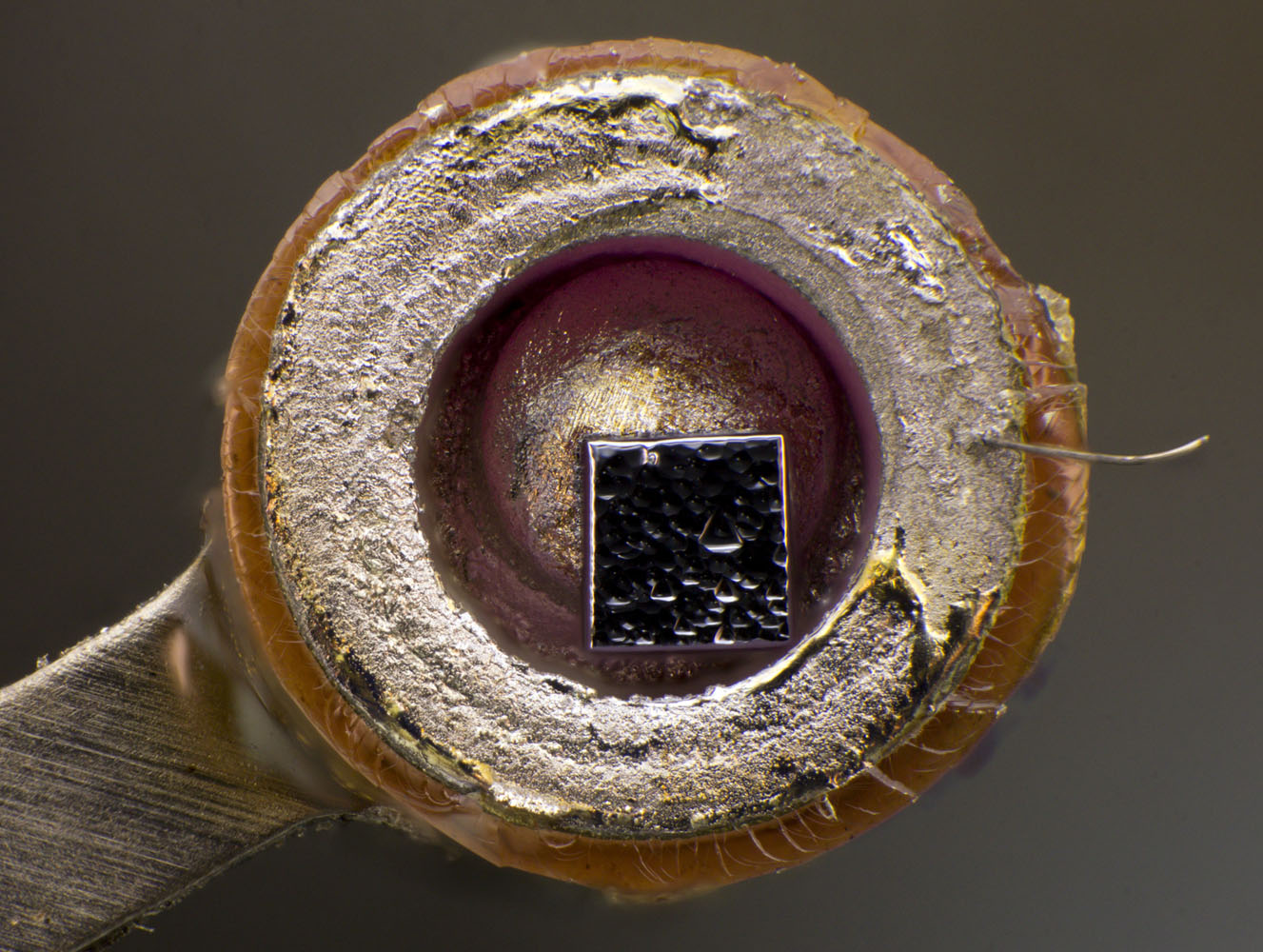


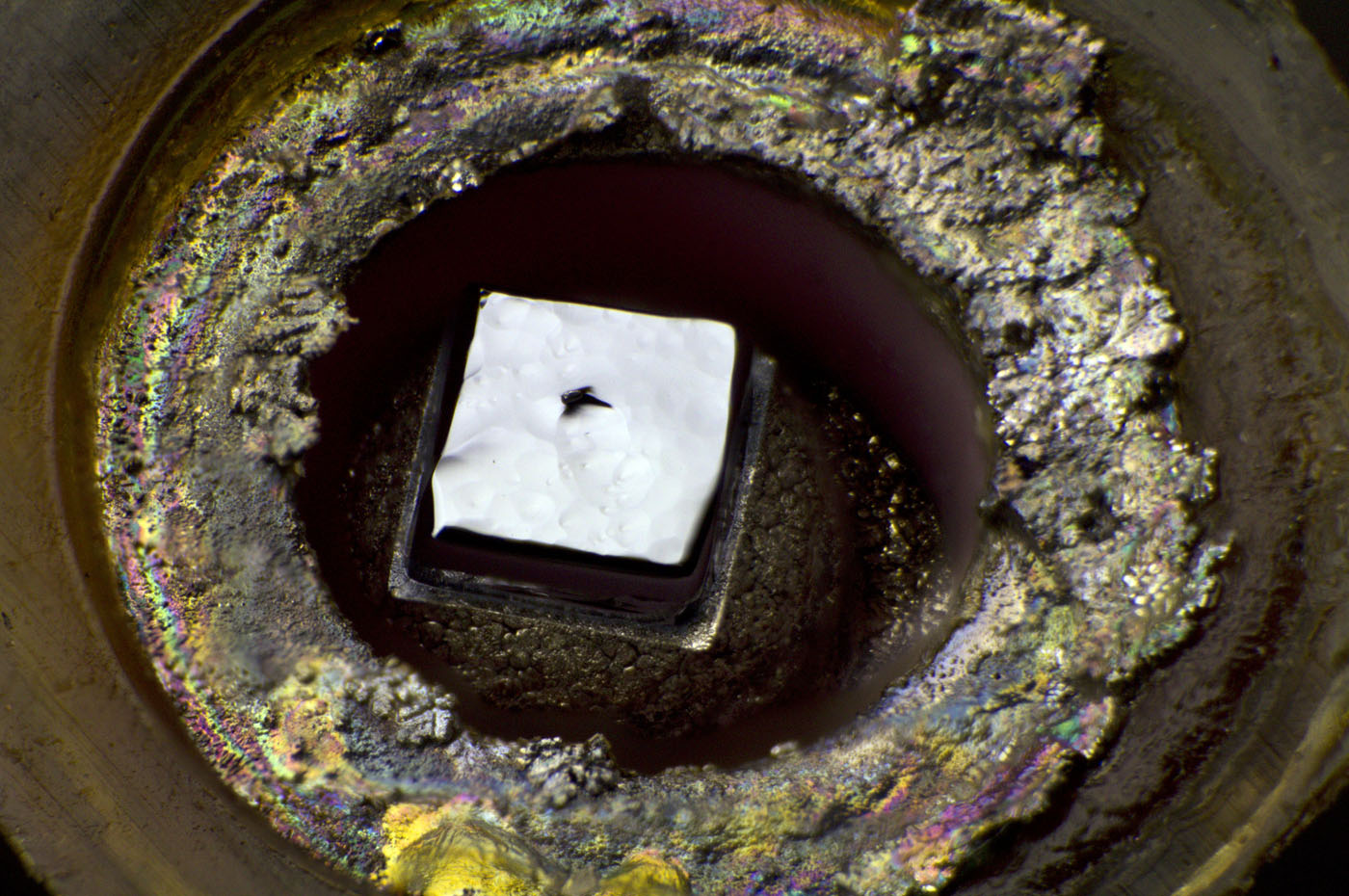
The semiconductor crystal is placed on a notch in the anode contact. In this part the crystal is placed off-center.

There is a wire connecting the crystal to the cathode which is torn off in this picture.
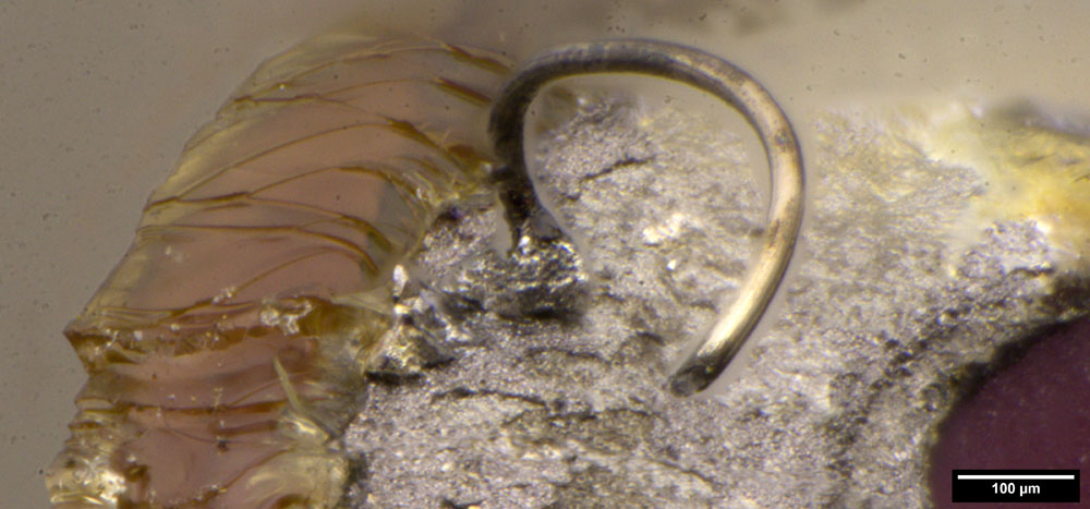


The diameter of the wire is ~30µm. The end is sharpened to reduce the contact area.
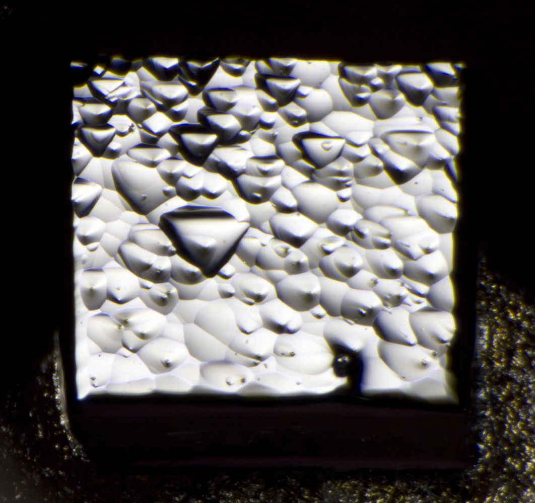


The edge length of the crystal is 0,7mm. The structure of the surface is due to etching which was done to remove impurities.
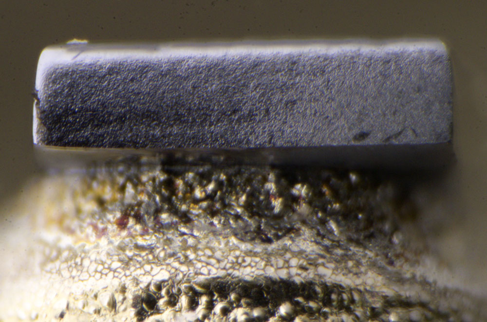
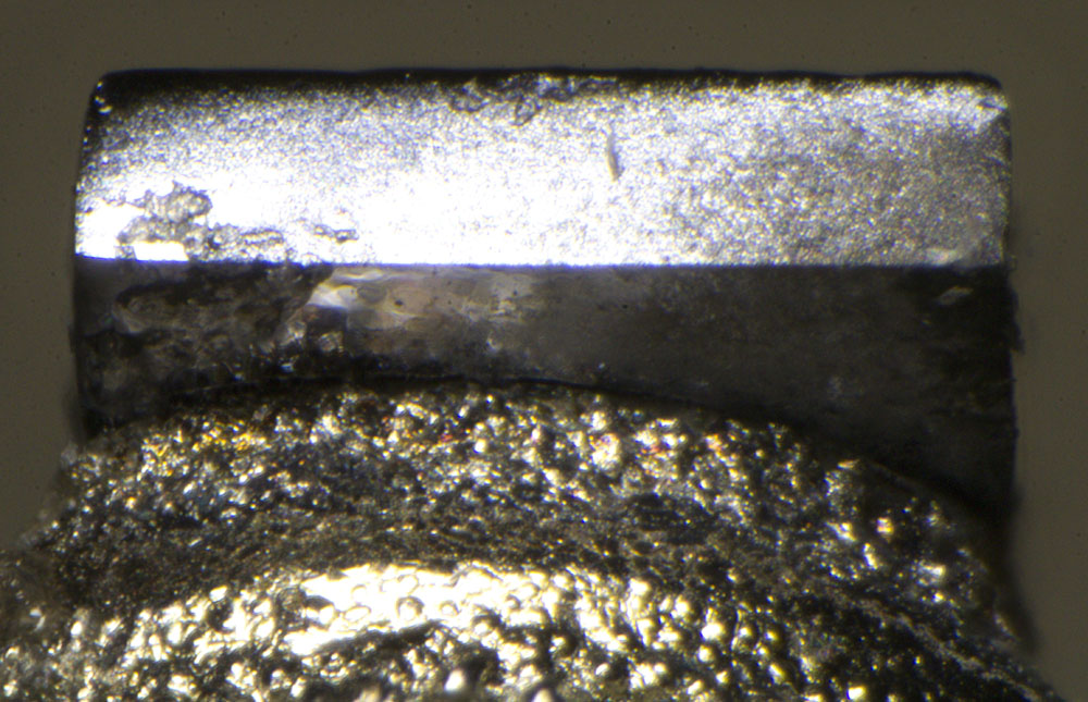


The die thickness is 0,2mm. Since it isn´t placed in the middle of the package we can take a look at the bottom of the crystal.
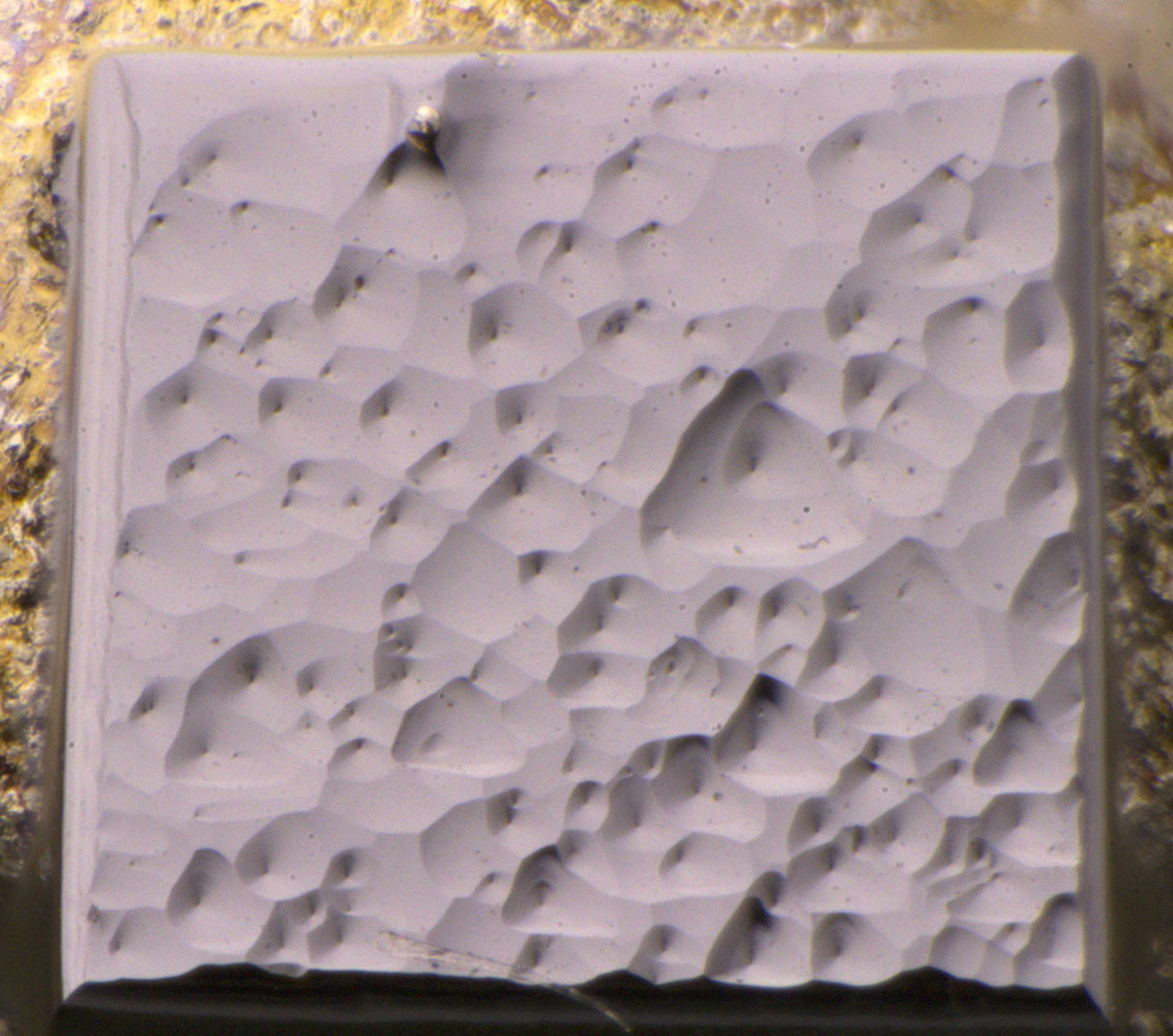
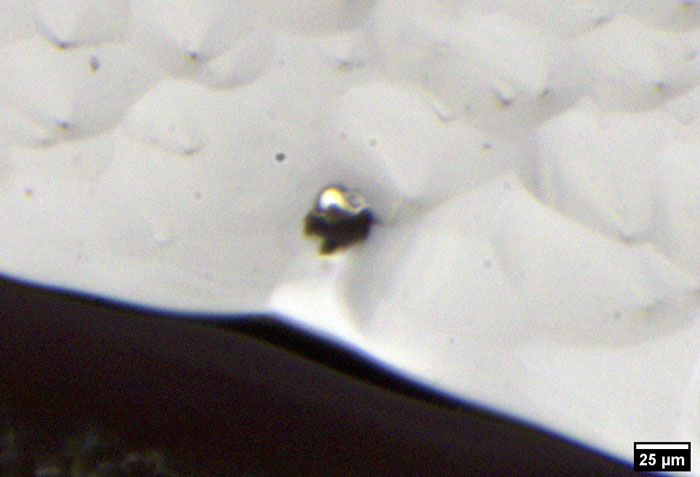


The pn junction must be highly doped in order to perform the function of a tunnel diode. For this reason, the junction cannot be constructed in the same way as for normal point-contact diodes. The high doping of a tunnel diode requires the direct alloying of an inverse doping agent, as it is done in alloy transistors. In the case of a tunnel diode, however, care must be taken to keep the alloying process short in order to produce as abrupt a pn transition as possible.

At the same time, it is important to keep the parasitic capacitance of the pn junction low. The alloy pill seen here therefore has a diameter of just 25µm. To further reduce the capacitance, one can etch down the semiconductor crystal after the alloying process to create a MESA structure. The remaining pillar is then very thin and correspondingly sensitive to mechanical and electrical stress. The GI308 mentioned above uses such a structure.
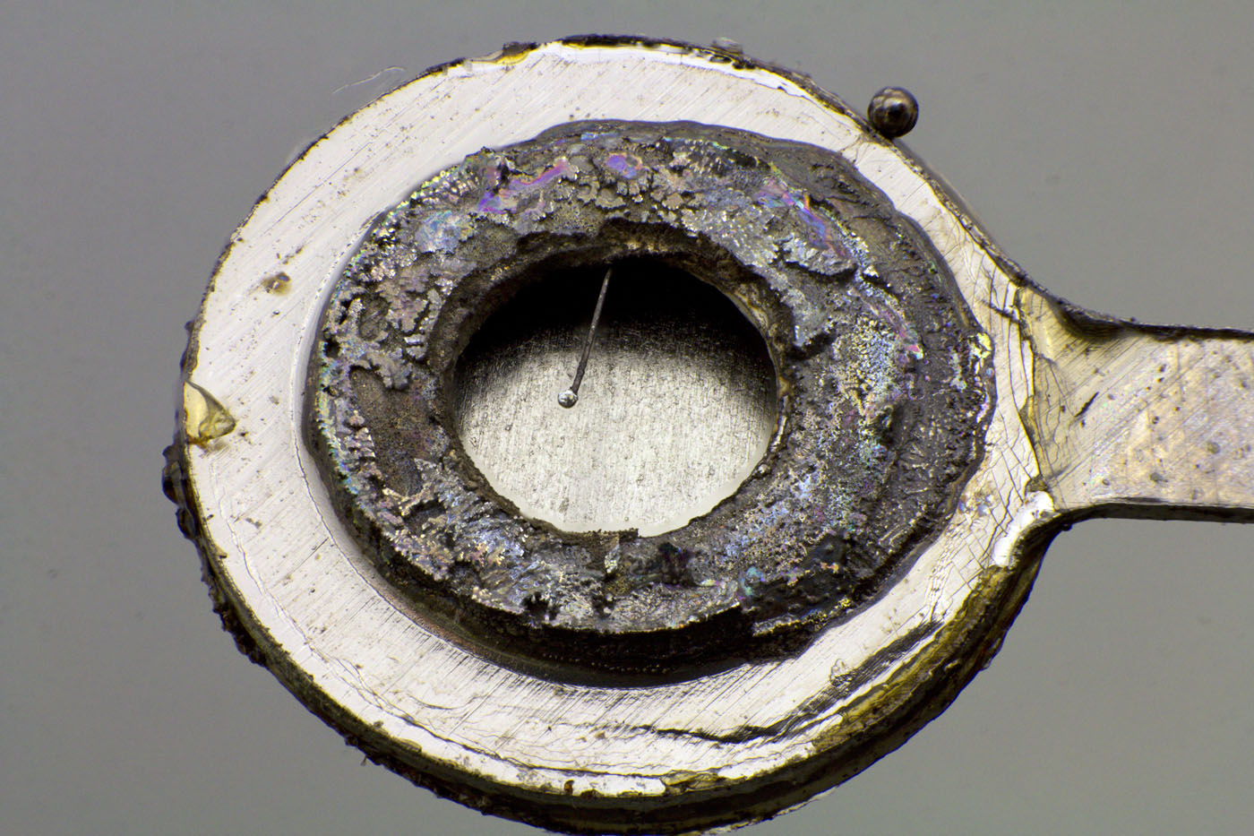


Another AI201G with a more acurate placed crystal. Here you can see how the bondwire is aranged.
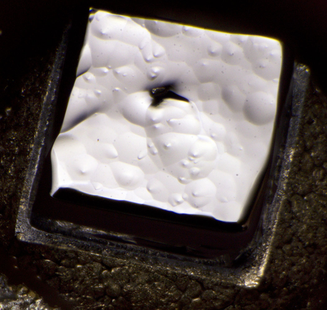
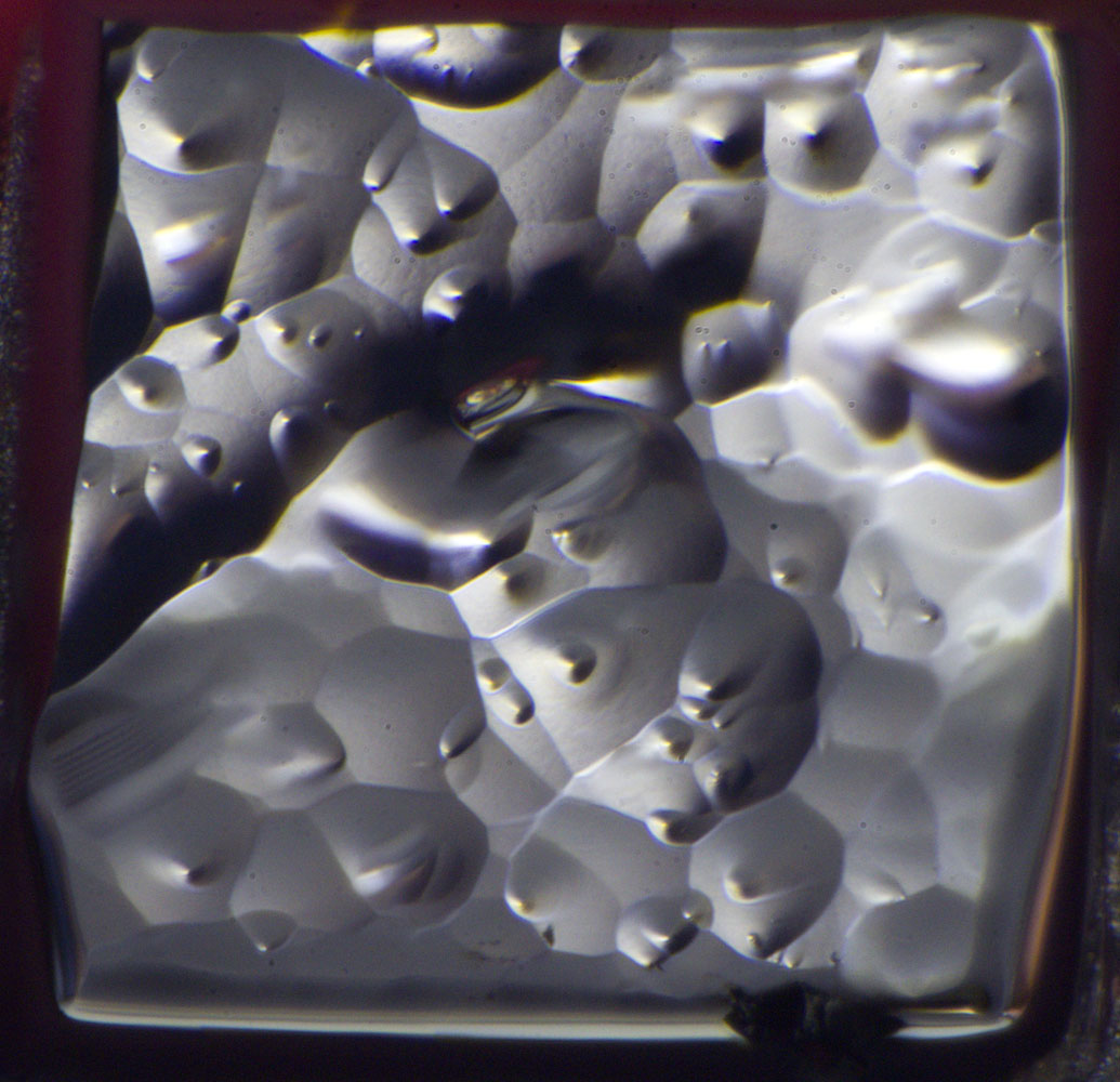


It looks like here the doping area is a little bigger (~40µm).
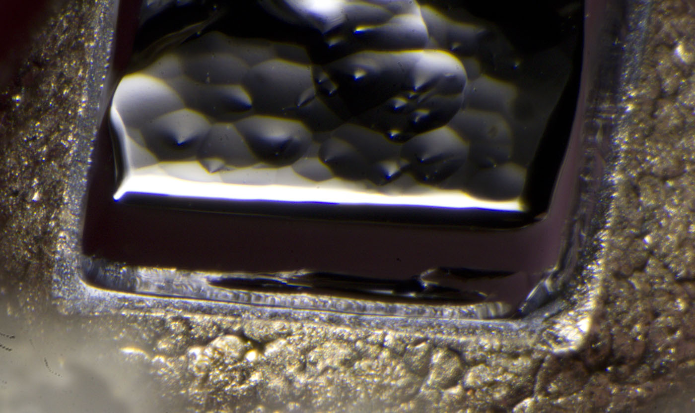


This diode is placed on some kind of a socket.


https://www.richis-lab.de/Diode07.htm

 :-/O
 
The following users thanked this post: SeanB, edavid, harrimansat, Gyro, RoGeorge, capt bullshot, iMo

Offline RoGeorge

  • Super Contributor
  • ***
  • Posts: 6636
  • Country: ro
Re: Diodes - die pictures
« Reply #27 on: May 08, 2022, 01:00:15 pm »


That's exactly how tunneling works!  :)

Offline NoopyTopic starter

  • Super Contributor
  • ***
  • Posts: 1867
  • Country: de
    • Richis-Lab
Re: Diodes - die pictures
« Reply #28 on: May 08, 2022, 01:05:45 pm »
Absolutely right: you have to be fast enough for tunneling!  :-+ :D

Offline Miyuki

  • Frequent Contributor
  • **
  • Posts: 907
  • Country: cz
    • Me on youtube
Re: Diodes - die pictures
« Reply #29 on: May 08, 2022, 02:46:27 pm »
What causes them to "wear out" and lose parameters over time?
It is some diffusion issue?
 

Offline NoopyTopic starter

  • Super Contributor
  • ***
  • Posts: 1867
  • Country: de
    • Richis-Lab
Re: Diodes - die pictures
« Reply #30 on: May 08, 2022, 03:03:57 pm »
What causes them to "wear out" and lose parameters over time?
It is some diffusion issue?

As far as I know driving them at high currents (within the specs) degenerates the junction. The ultra high doping around the abrupt junction tends to mix to a rather normal junction.

I have ordered one of these MESA type tunnel diodes. Their small area (high current density) made them especially sensitive.

The alloy process was pretty tricky. Heating and cooling had to be very fast.

Offline David Hess

  • Super Contributor
  • ***
  • Posts: 17065
  • Country: us
  • DavidH
Re: Diodes - die pictures
« Reply #31 on: May 09, 2022, 06:51:12 am »
What causes them to "wear out" and lose parameters over time?
It is some diffusion issue?

As far as I know driving them at high currents (within the specs) degenerates the junction. The ultra high doping around the abrupt junction tends to mix to a rather normal junction.

Then why do silicon tunnel diodes not degrade under the same conditions?  Are they different in requiring a lower current density in operation?
 

Offline T3sl4co1l

  • Super Contributor
  • ***
  • Posts: 22288
  • Country: us
  • Expert, Analog Electronics, PCB Layout, EMC
    • Seven Transistor Labs
Re: Diodes - die pictures
« Reply #32 on: May 09, 2022, 07:05:38 am »
Silicon diffuses slower at a given temp?

Tim
Seven Transistor Labs, LLC
Electronic design, from concept to prototype.
Bringing a project to life?  Send me a message!
 

Offline NoopyTopic starter

  • Super Contributor
  • ***
  • Posts: 1867
  • Country: de
    • Richis-Lab
Re: Diodes - die pictures
« Reply #33 on: May 09, 2022, 09:17:54 am »
Silicon diffuses slower and I assume it´s also due to more modern technology.

Back in the days there were no Si tunnel diodes, just GaAs and Ge and we know these old diodes are pretty touchy.

Nowadays it seems like we can make everything possible and I´m sure there is some magic put into modern Si tunnel diodes.

Online Kleinstein

  • Super Contributor
  • ***
  • Posts: 14666
  • Country: de
Re: Diodes - die pictures
« Reply #34 on: May 09, 2022, 01:52:07 pm »
Diffusion in germanium is relatively fast. It is not just the tunnel diodes that wear out. Germanium transitors are also known for aging.Germanium detectors for gamma / X-ray spectroscopy even need cooling well below room temperature just for storrage.
 

Offline NoopyTopic starter

  • Super Contributor
  • ***
  • Posts: 1867
  • Country: de
    • Richis-Lab
Re: Diodes - die pictures
« Reply #35 on: June 07, 2022, 11:31:01 am »
Just a small update regarding the point contact diode.


Dr. Matthias Falter describes in his book "Dioden- und Transistortechnik" that due to surface effects in every n-doped semiconductor negative charges are pushed away from the surface. If you have a n-type semiconductor with some p-doping in it you automatically get an pn-junction.

The fusing of the point contact diode amplifies the effect. I melts the Ge and the electric field moves n-dopant into the crystal while it moves p-dopant to the surface.


https://www.richis-lab.de/Diode05.htm#Spitzendiode

 :-/O
 
The following users thanked this post: exe

Offline NoopyTopic starter

  • Super Contributor
  • ***
  • Posts: 1867
  • Country: de
    • Richis-Lab
Re: Diodes - die pictures
« Reply #36 on: November 02, 2022, 07:51:39 pm »


You can find no direct information about the NT-1103. The designation indicates that the manufacturer was the German company Nortron. Datasheets still exist for a few diodes with similar designations. There are hints that the NT-1103 is a Zener diode with a Zener voltage of 3,9V. On the present model the breakdown voltage is 3,75V (5mA). The forward voltage is 0,64V (5mA).


The structure appears quite crude. It is an n-doped silicon die alloyed with a piece of aluminum. The aluminum serves as a p-dopant, resulting in the desired pn structure.


The silicon wafer is about 0,16mm thick. It is mounted on a metal plate, which in turn is soldered to the contact pin.


The surface of the silicon wafer is very smooth also at the lateral edges. Apparently, it was subjected to an etching process after being cut into this shape. This cleans the surface and reduces the imperfections. At the front corner, however, a piece broke out afterwards.

Finally, the diode was protected against the environmental conditions with a varnish.


The contact area is located in a recess. The alloying of aluminum was not done with the large aluminum element. With such a large mass, it would be difficult to adjust the alloying process precisely and reproducibly. For this reason, an additional aluminum layer about 15µm high was deposited on the silicon surface instead, which was used for alloying. Later the large aluminum element was joined.


https://www.richis-lab.de/Diode08.htm

 :-/O
 
The following users thanked this post: SeanB, exe, RoGeorge, iMo, D Straney

Offline NoopyTopic starter

  • Super Contributor
  • ***
  • Posts: 1867
  • Country: de
    • Richis-Lab
Re: Diodes - die pictures
« Reply #37 on: November 11, 2022, 09:11:02 pm »


S2 is the SMD marking of the varactor diode BBY40.
We don´t know the manufacturer. The pinning shown here is taken from the NXP datasheet.


The edge length of the die is 0,4mm. There are a lot of edges at the edges of the die. ;D Perhaps that is due to the special doping distribution that is very important in a good varactor diode.

I don´t know why there is just one round corner.  :-//


https://www.richis-lab.de/Diode09.htm

 :-/O
 
The following users thanked this post: SeanB, exe, RoGeorge

Offline NoopyTopic starter

  • Super Contributor
  • ***
  • Posts: 1867
  • Country: de
    • Richis-Lab
Re: Diodes - die pictures
« Reply #38 on: January 08, 2023, 08:26:40 pm »


Just a small ZD15, a 15V Z-diode.


The semiconductor is cylindrical. On one side, it is connected flatly to one of the contact elements. On the other side, there is a thin metal pin between the semiconductor and the contact element.

The sheet metal parts are surprisingly large. The curved contact could be intended to absorb thermomechanical stresses. The large surfaces should also improve heat dissipation.


The semiconductor itself has a diameter of 0,9mm and a length of 0,8mm. The surface is rough and does not reveal any special structures.


The surface on which the semiconductor is contacted by the metal pin is covered with a silicone-like material. No special structure can be seen at the junction. Thus, it remains unclear how exactly the Z-diode is constructed.


https://www.richis-lab.de/Diode10.htm

 :-/O
 
The following users thanked this post: SeanB, RoGeorge, iMo

Online iMo

  • Super Contributor
  • ***
  • Posts: 5071
  • Country: bt
Re: Diodes - die pictures
« Reply #39 on: January 08, 2023, 08:39:30 pm »
Isn't it a piston from Titanic's steam engine ? :)
 

Offline RoGeorge

  • Super Contributor
  • ***
  • Posts: 6636
  • Country: ro
Re: Diodes - die pictures
« Reply #40 on: January 08, 2023, 08:42:01 pm »
Was the Zener working before decapping?

Offline NoopyTopic starter

  • Super Contributor
  • ***
  • Posts: 1867
  • Country: de
    • Richis-Lab
Re: Diodes - die pictures
« Reply #41 on: January 08, 2023, 08:51:01 pm »
Isn't it a piston from Titanic's steam engine ? :)

Indeed!  :-+ ;D


Was the Zener working before decapping?

I can´t tell with 100% certainty but it should have been ok before decapping.

Offline NoopyTopic starter

  • Super Contributor
  • ***
  • Posts: 1867
  • Country: de
    • Richis-Lab
Re: Diodes - die pictures
« Reply #42 on: January 08, 2023, 08:57:23 pm »
Oh, wait a minute! I think I was wrong!  |O

I got this part from the Tele Quarz Group CCO 200: https://www.richis-lab.de/osc_03.htm
Back then I wondered why the voltage rating of this Z-Diode is that high but now I think that is no zener but a tantalum capacitor with 15µF! That would explain why there is no junction...  ;D
 
The following users thanked this post: SeanB, Zoli

Offline T3sl4co1l

  • Super Contributor
  • ***
  • Posts: 22288
  • Country: us
  • Expert, Analog Electronics, PCB Layout, EMC
    • Seven Transistor Labs
Re: Diodes - die pictures
« Reply #43 on: January 08, 2023, 09:20:07 pm »
 :-DD

I mean... it's sort of a diode, right? It's polarized, right?

:P Tim
Seven Transistor Labs, LLC
Electronic design, from concept to prototype.
Bringing a project to life?  Send me a message!
 

Offline NoopyTopic starter

  • Super Contributor
  • ***
  • Posts: 1867
  • Country: de
    • Richis-Lab
Re: Diodes - die pictures
« Reply #44 on: January 08, 2023, 09:30:12 pm »
Absolutely! It acts differently with different polarities, it´s kind of a diode!  ;D

Offline exe

  • Supporter
  • ****
  • Posts: 2607
  • Country: nl
  • self-educated hobbyist
Re: Diodes - die pictures
« Reply #45 on: January 09, 2023, 01:47:26 pm »
Tantalums also have sound visual polarity indication. I once reverse biased it and it blew in my face with a bang  |O
 
The following users thanked this post: SeanB

Offline NoopyTopic starter

  • Super Contributor
  • ***
  • Posts: 1867
  • Country: de
    • Richis-Lab
Re: Diodes - die pictures
« Reply #46 on: January 09, 2023, 05:18:43 pm »
Tantalums also have sound visual polarity indication. I once reverse biased it and it blew in my face with a bang  |O

 ;D
Yes, they give a very clear feedback!  :-+

Offline SeanB

  • Super Contributor
  • ***
  • Posts: 16362
  • Country: za
Re: Diodes - die pictures
« Reply #47 on: January 12, 2023, 12:11:22 pm »
Just do not do that with 4700uf 35V tantalum block units, they internally contain a pcb with a load of smaller tantalum capacitors on it, then are potted in soft silicone and then soldered shut. They do go bang nicely, and with a few blasts as well. Never got to do that with the monolithic 10 000uF round ones, though I suspect that would result in a lot of shrapnel, as those are pretty big, and also pretty expensive as well.
 

Offline mister_rf

  • Contributor
  • Posts: 33
  • Country: ro
Re: Diodes - die pictures
« Reply #48 on: January 17, 2023, 12:00:36 pm »
Many beautiful pictures posted here.
I will post some of the pictures I took.  :)

EFD108 is a germanium point contact diode in a DO-7 type package.


The following users thanked this post: SeanB, RoGeorge, floobydust, Miyuki

Offline RoGeorge

  • Super Contributor
  • ***
  • Posts: 6636
  • Country: ro
Re: Diodes - die pictures
« Reply #49 on: January 17, 2023, 12:26:20 pm »
That's a very good looking pic.  :-+
Lens?  Camera? Photo stacking?


Share me

Digg  Facebook  SlashDot  Delicious  Technorati  Twitter  Google  Yahoo
Smf