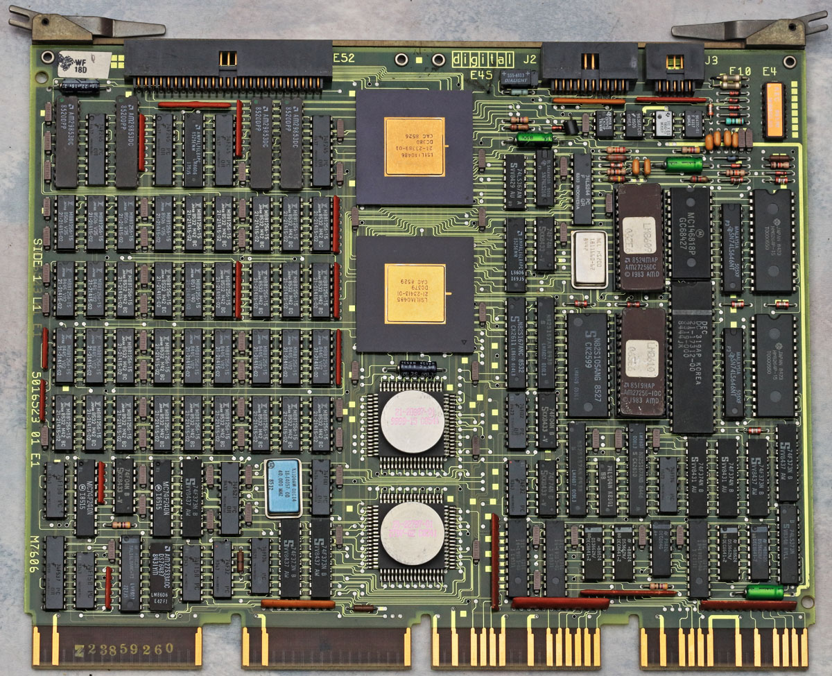
The board shown here with the designation KA630 is a CPU module of the MicroVAX II. The MicroVAX computer systems were developed by DEC (Digital Equipment Corporation) and are successors of the VAX-11 model series. The MicroVAX I was the first generation, followed by the MicroVAX II.
The "Digital Technical Journal" published by DEC in March 1986 explains many details of the MicroVAX II. According to this, the focus of the development was to integrate as many CPU functions as possible, which were previously distributed over many integrated circuits, into one microprocessor. This development was necessary to remain competitive.
The first mask set of the 78032 was developed in 20 months, according to Digital Technical Journal. It took 6 months to establish the requirements and basic design. The development of the actual circuit required 14 months. The goal was to mass produce the IC after two and a half years at the latest.
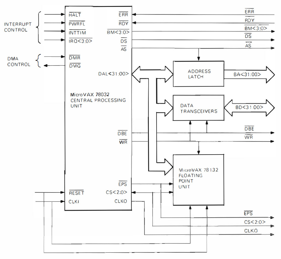
The Digital Technical Journal contains the above illustration of the KA630 board. The core of the board is the 78032 CPU and the 78132 FPU, with two gate arrays above them. The lower gate array is tightly coupled to the CPU. The upper gate array is the interface to the Q22 bus, which connects the CPU board to the other modules. A full integration of the VAX architecture would have required 1,25 million transistors. However, the technology at the time only allowed one tenth of this to be integrated into the microprocessor. Therefore, compromises had to be made in the degree of integration.
On the left, 36 256kBit DRAM devices are populated, providing a total of 1MB of RAM. The Digital Technical Journal reports a shortage of 256kBit devices at the time of development, so an alternative assembly with 64kBit memory was planned. You can expand the working memory up to 16MB with expansion cards.
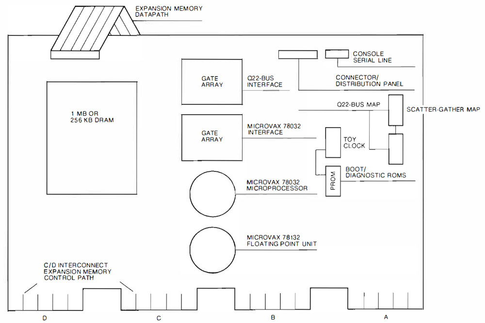
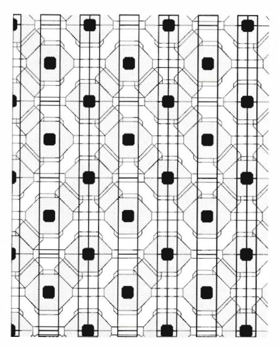
The "KA630-AA CPU Module User's Guide" contains a block diagram that shows the architecture of the CPU board in more detail.
The 78032 CPU and 78132 FPU are placed in a TQFP-68 package with a round heat sink.
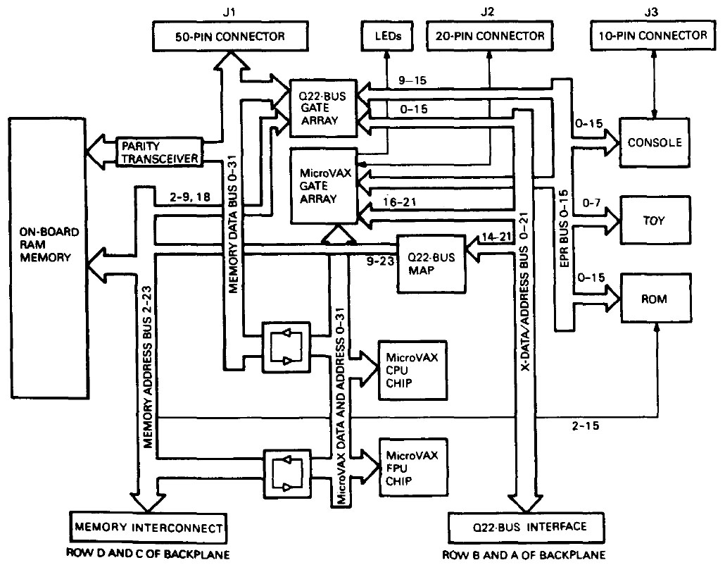
The 78032 was just used by DEC itself. Therefore it is not surprising that no datasheet exists. The above block diagram from the Digital Technical Journal is the most detailed representation that can be found.
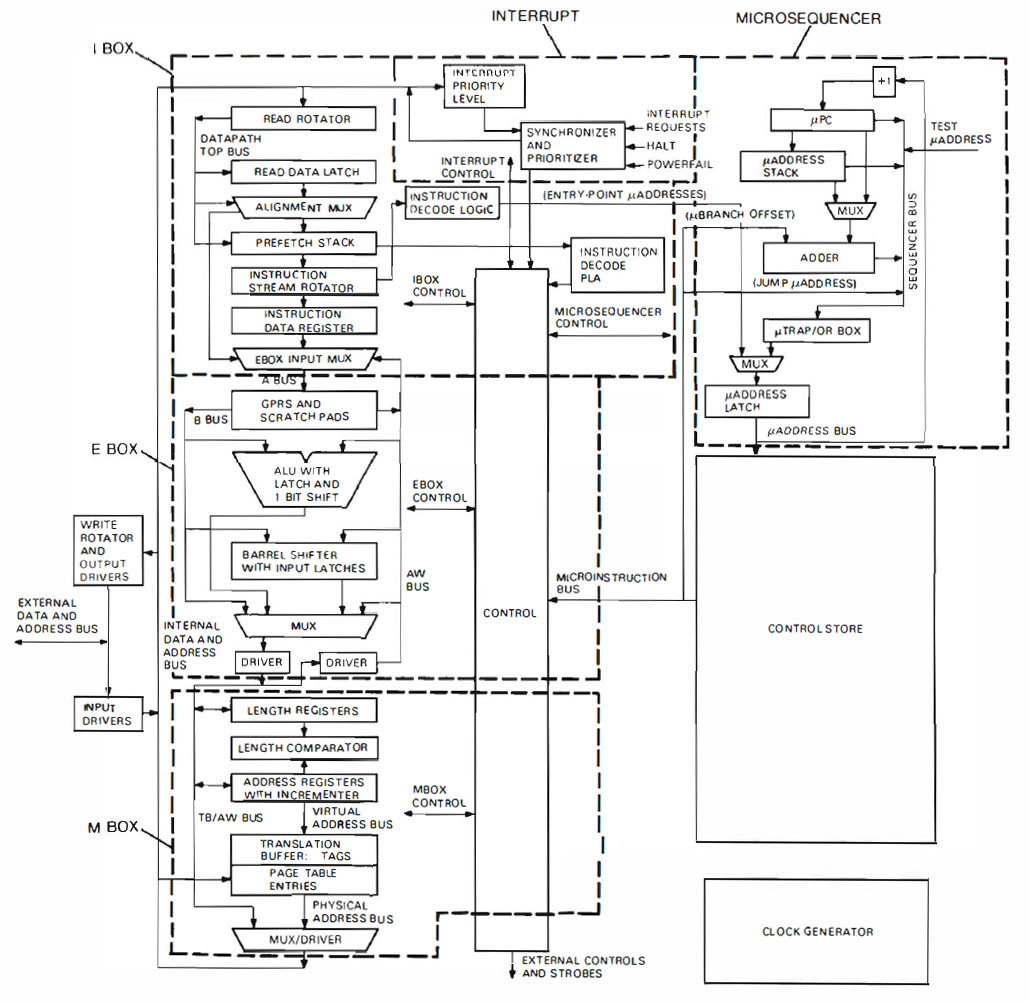
The integrated function blocks are presented in great detail in the Digital Technical Journal.
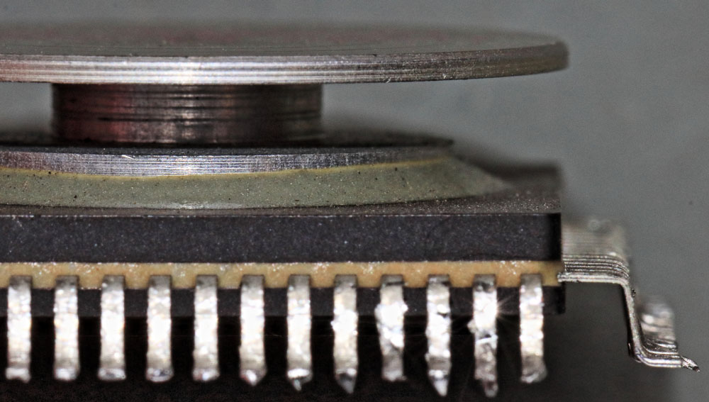
The heatsink is glued onto the ceramic package. The CPU operates with 5V and a clock frequency of 20MHz. This typically results in 3W of power dissipation.
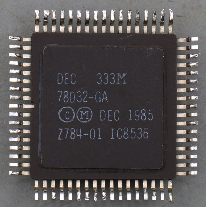
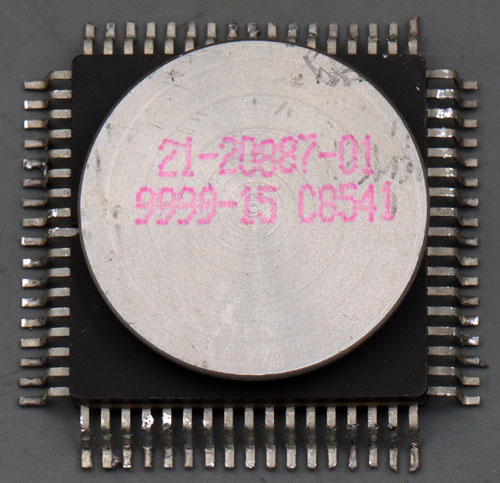
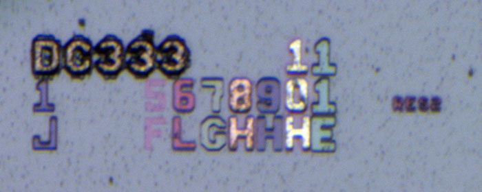
The inscription can be found on the underside of the case. The numbers 8536 in the lower right corner probably represent the datecode. The string 333M refers to the internal designation DC333.
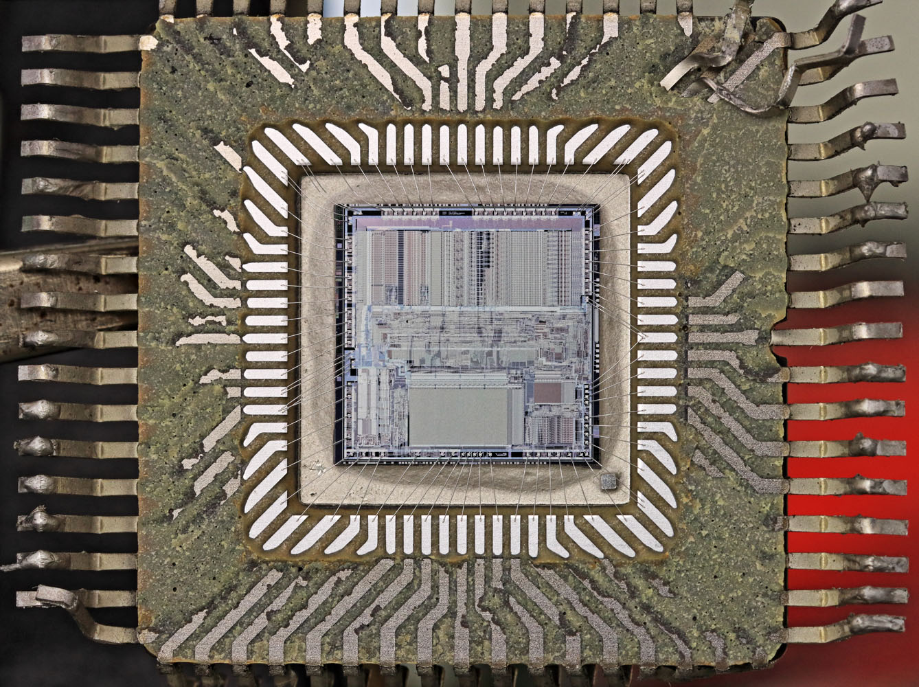
The die is fixed in the upper half of the case. This allows the heat to be efficiently dissipated through the top of the package.
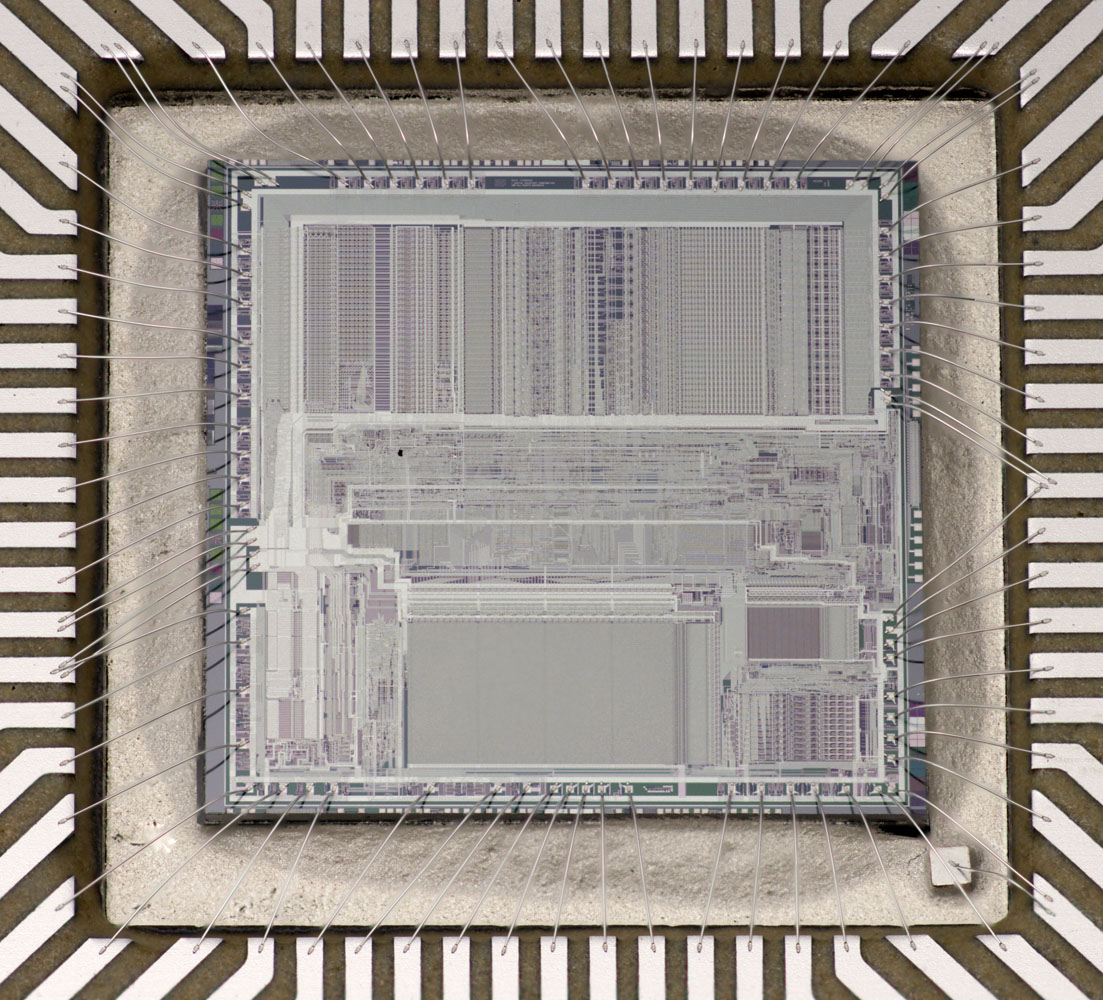
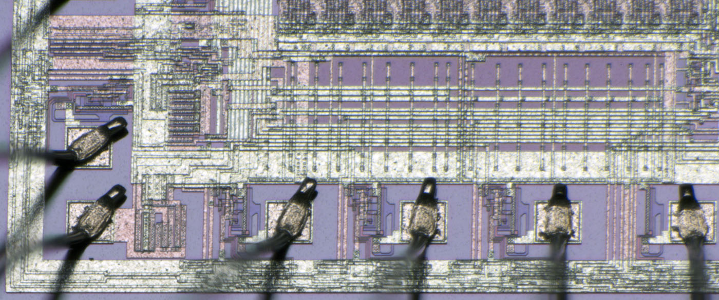
In the overview, it is noticeable that special attention was paid to an interference-free supply of the individual function blocks. The outer areas of he upper half of the die contains the wide data and address interface. These drivers have their own wide supply lines, which are routed to four pins in each of the two corners with two bondwires. The supply pins in the middle of the left and right side supply the actual CPU via two bondwires each. The interfaces in the lower half partly have their own bondwires again, but they are not as exclusively supplied as the upper interfaces.
A small cuboid in the lower right corner puts the potential of the carrier and thus also of the substrate to a pin, which in turn is connected to a bondpad.
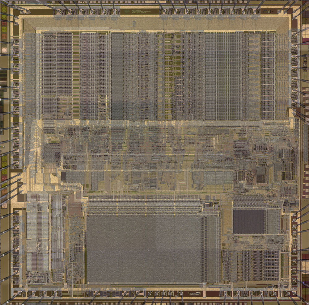
The die measures 9,1mm x 9,0mm. The Digital Technical Journal gives a size of 8,7mm x 8,6mm, which is the size without the remainings of the frame structure. The Digital Technical Journal further describes that 125.000 transistors were integrated. A 3µm NMOS process with two metal layers was used, which DEC called ZMOS.
The picture shown here is also available in higher resolution (102MB):
https://www.richis-lab.de/images/cpu/04x10XL.jpg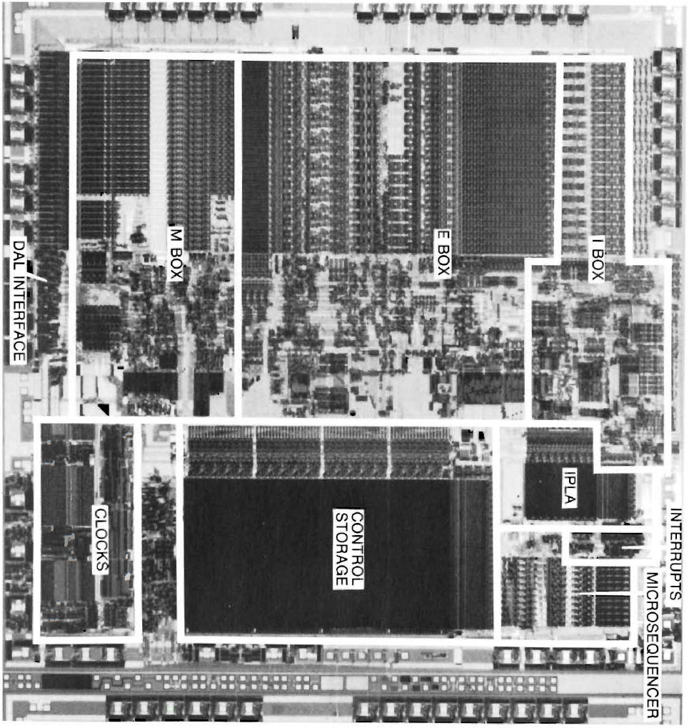
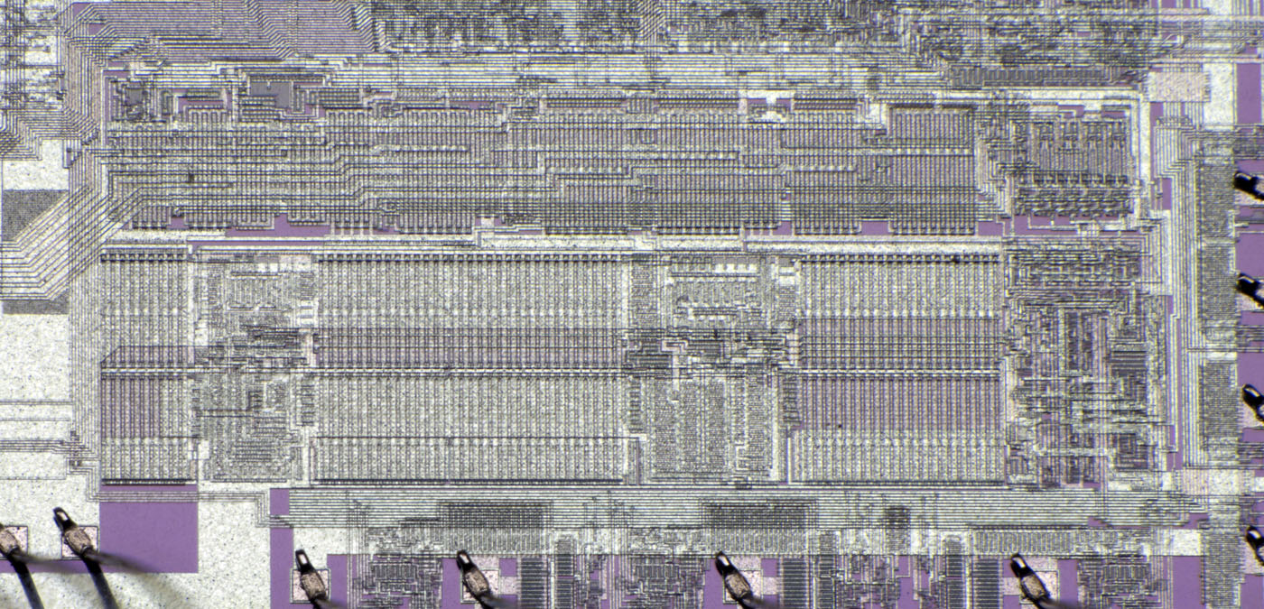
The Digital Technical Journal shows the distribution of the function blocks on the die. Obvious is the very large ROM in the lower area that converts the commands into the necessary control signals. The core of the CPU, here called I-Box, E-Box and M-Box, is very large due to the 32Bit wide structures and including the control circuits takes up more than half of the area.
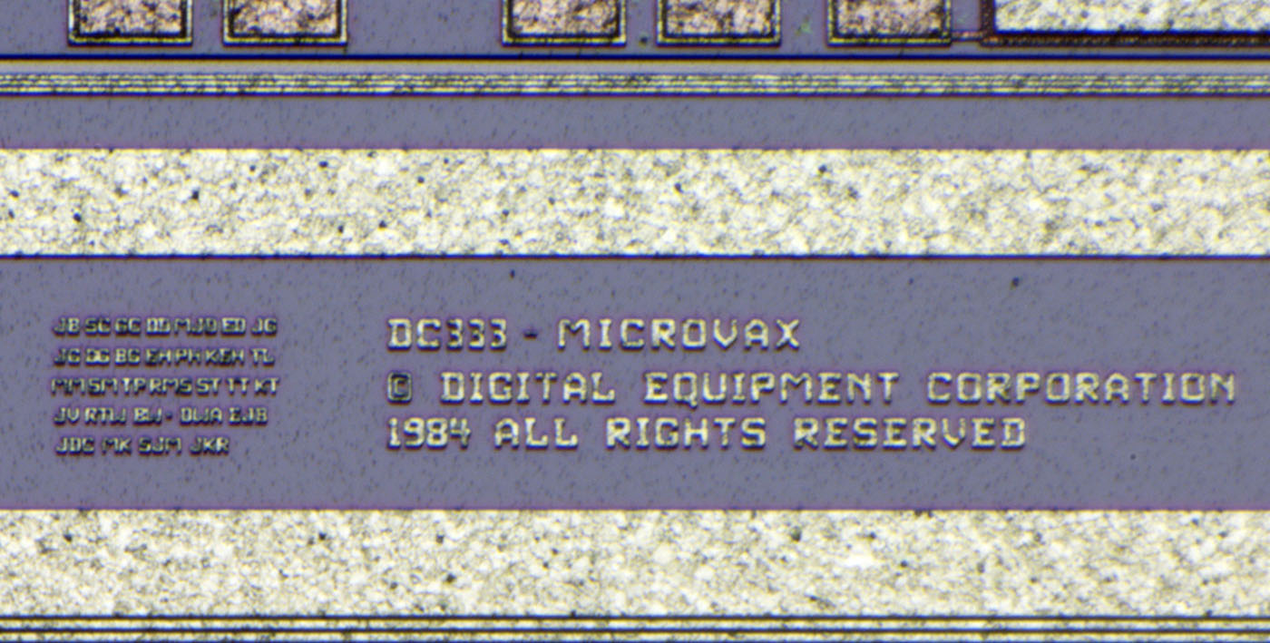
On the upper edge there is a copyright from 1984 and the internal designation DC333. The letters in the left area are certainly abbreviations of the developers. The Digital Technical Journal reports 18 developers who worked on the 78032.
Eight masks are directly visible. As far as the letters indicate revisions, the design was revised nine times. In contrast, the Digital Technical Journal praises "very very few bugs", in detail it would have been "less than 20 bugs" until it was possible to boot the operating system.
The two metal layers 8 and 10 are nicely visible here. The mask 7 creates contacts to the silicon. The upper metal layer can only contact the lower metal layer, for which mask 9 is used. Mask 11 then creates openings in the passivation layer where the bondpads are located.
In addition to the masks of the metal layers, just three visible masks remain. It can be assumed that other masks were used between 1 and 5. The Digital Technical Journal describes four transistor types that were available in this process: N, E (light enhancement), L (light depletion) and D.
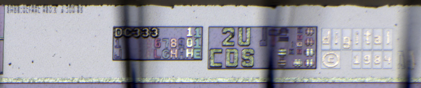
In the frame structure the designation and the revisions of the mask set are mapped one more time. 2U CDS could be a process designation.
A label is just visible in the upper left corner, apparently referring to the technology node. The lines start with ZMOS.ULTRAL and end with a date from 1983.
A test structure at the bottom edge contains several elements. The long stripes on the left seem to be resistors. The remaining structures represent different transistors.

A very wide test structure is integrated at the right edge. It remains unclear which function is shown here, but it seems there are a lot of identical elements connected in series. Perhaps several gates were connected in series to check their quality with a test signal.
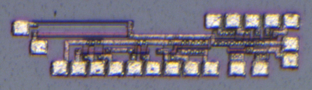
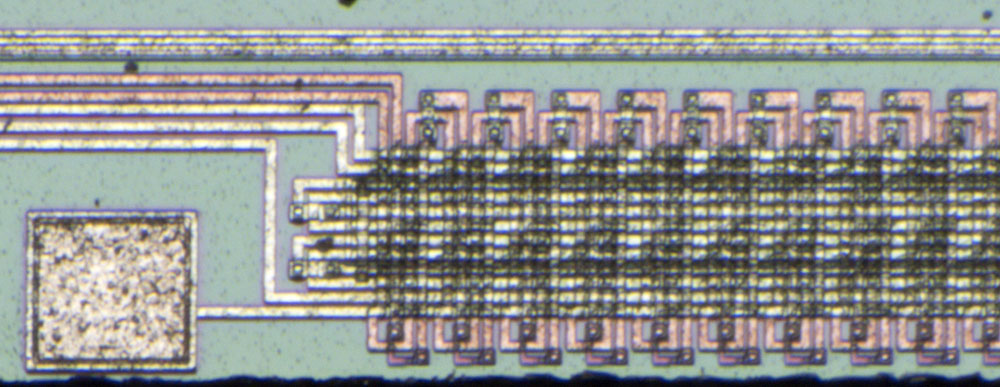
In the lower right corner (rotated here) is a bias generator, like the ones found in the µPD7220 (
https://www.richis-lab.de/GraKa02.htm#bias) and the D82720 (
https://www.richis-lab.de/GraKa03.htm#bias). It is a charge pump that generates a negative potential. Directly visible is the relatively large capacitor, which is contacted with many vertical leads. The negative potential is transferred via the cuboid next to the die to the carrier and thus to the substrate. The negative body potential improves the switching behavior of the transistors.
In the lower left corner of the die the clock processing is located, which takes up a relatively large area (rotated here). A 40MHz clock must be supplied from the outside. The Digital Technical Journal explains that eight phase-shifted clocks are generated from this clock. The drivers have to be partly very powerful, because they have to drive up to 250pF.
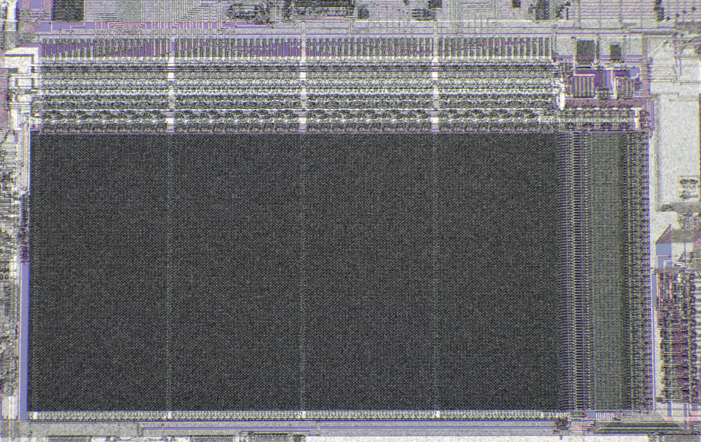
The layout of the large ROM is given by the Digital Technical Journal as 1600 x 39Bit.
As already described, the reduction of transistor and area consumption was a critical requirement. The optimized arrangement of the control commands in the control ROM brought relief. The Digital Technical Journal additionally highlights the X-shaped memory cells with their reduced area consumption.
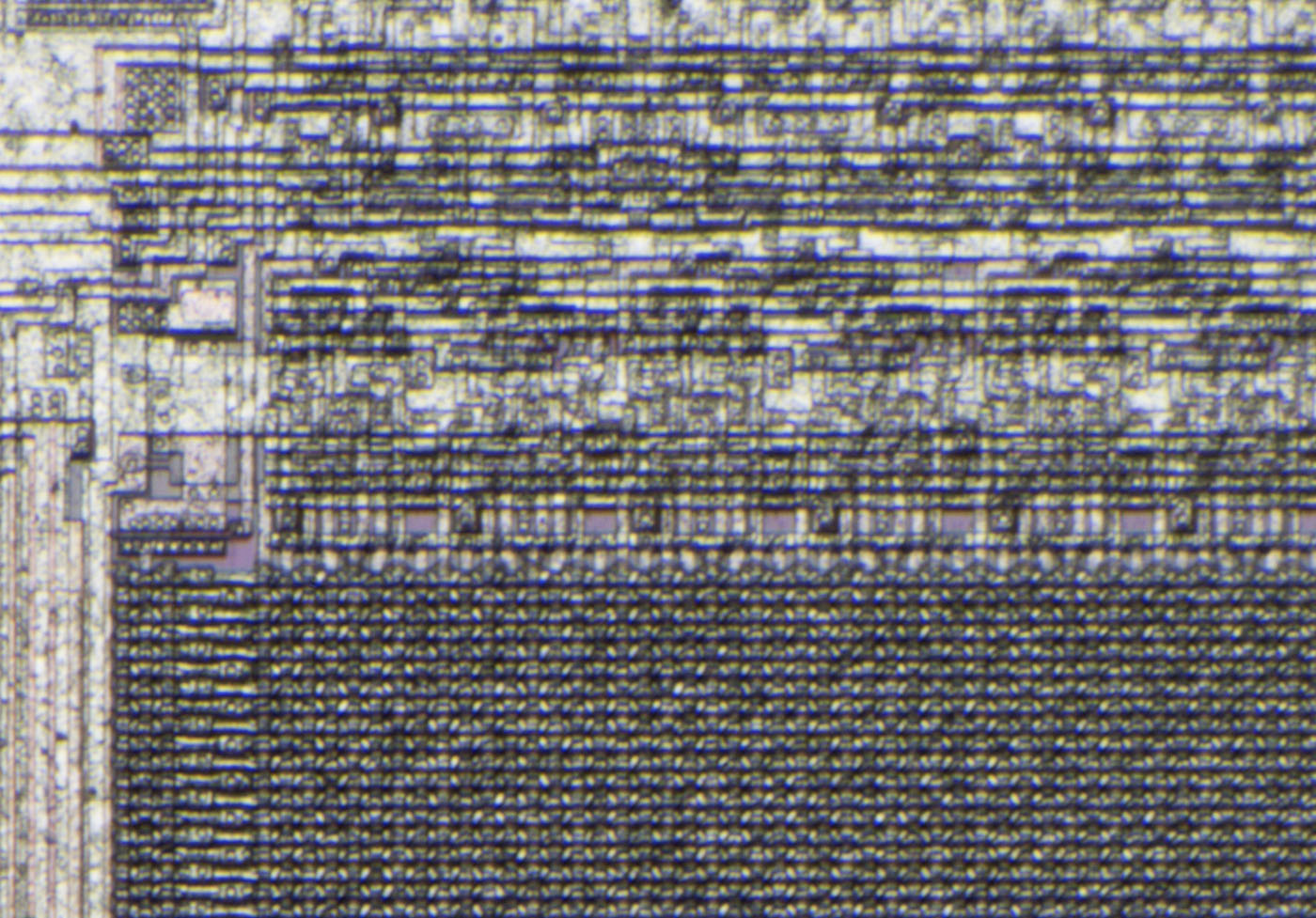
I can´t resolve the relatively complex structures of the memory.
https://www.richis-lab.de/cpu04.htm 


