This collection can be found in the Thuringian Museum of Electrical Engineering (
https://www.elektromuseum.de/). It shows the various processing steps in the manufacture of the U809M.
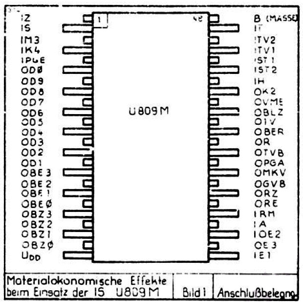
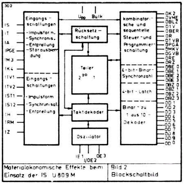
The U809M is a special circuit and you don´t find very much information about it. In the component comparison list of the Kombinat Mikroelektronik it is listed under the designation "Vermittlungs IS" for telephone systems. The above two pictures are taken from the paper "Materialökonomische Effekte beim Einsatz der IS U809M". This paper was shown in 1983 at the "Halbleiterbauelemente-Symposium", which was regularly organized by the "Halbleiterwerk Frankfurt Oder".
The paper explains that the U809M is a customized circuit developed for the ATZ 65 automatic telephone exchange. The U809M replaces electromechanical assemblies. Using 10.000 of the integrated circuits could save 44kg of precious metal, 7t of nickel silver, 12t of copper and 19t of magnetic switch iron. The U809M was developed at Funkwerk Erfurt in cooperation with the Fernmeldewerk Anrstadt.
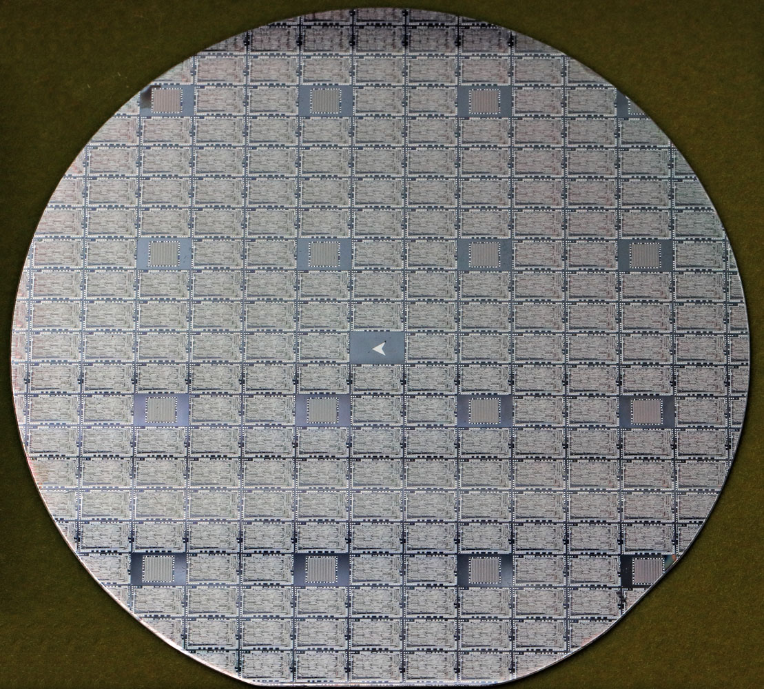
In the collection of the Thuringian Museum of Electrical Engineering there is a 3" wafer as a starting point. The flattening at the lower edge shows that it is a p-doped substrate with a (111) crystal structure. There are a relatively large number of test structures between the circuits. The wafer contains estimated 181 complete U809M circuits. The size of the U809M (5,5mm x 3,4mm) significantly reduces the yield. On a smaller 2" wafer, in contrast, it was possible to integrate 1128 of the comparatively much smaller D220 (edge length 1,2mm,
https://www.richis-lab.de/wafer01.htm).
The test structure has the designation MT7. MT seems to have been a standard designation for test structures. On the 4" wafer with the U3230 (
https://www.richis-lab.de/wafer04.htm), the test structures bear the designation MT21S.
The largest part of the area is taken up by a folded structure. Various small elements are integrated around the perimeter.
The folded test structure is quite complex. The part connected at the lower edge represents a large transistor. The rest seems to contain special forms of transistors or transistor-like structures.
At the right edge one can measure a series of vias. At the lower edge, a metal gate and a polysilicon gate MOSFET can be seen.
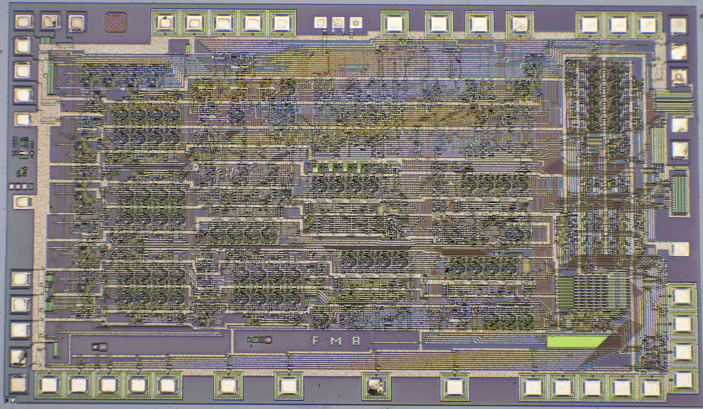
According to the Semiconductor Symposium paper the circuit measures 5,5mm x 3,4mm, contains 3191 transistors and is based on p-channel silicongate technology.
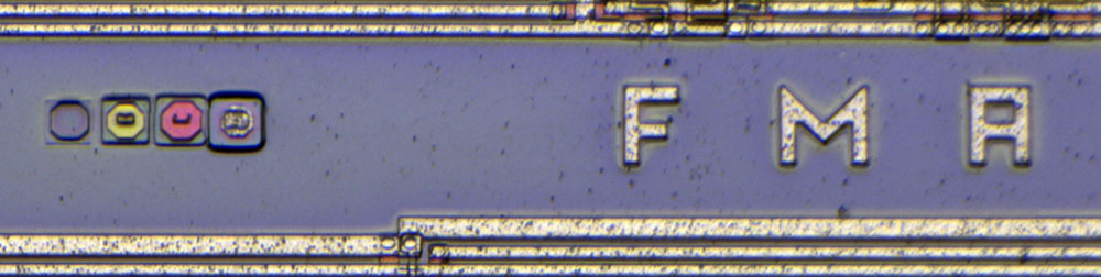
At the bottom of the die there are the letters FMA, which could be a clue to the developers.
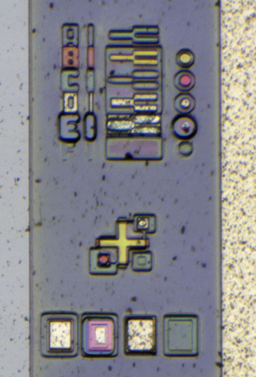
On the left edge of the die you can see the masks used and their revisions: A1, B1, C1, D1, E1 and F1. Mask A1 opens the field oxide (FOX), which initially protects the wafer and thus defines the active areas. B1 then structures the polysilicon. The polysilicon appears red on the FOX, while it appears yellowish in the active area.
After the polysilicon a full-surface n-dopant is applied, which penetrates into the open active regions. These areas are then isolated from the p-doped substrate. Where the polysilicon is located above the active areas, the n-doping is shielded so that the PMOS transistors form underneath. This simultaneously ensures that the polysilicon gate is directly above the p-channel ("self-aligned gate").
D1 is the metal layer, so C1 must be the mask for the vias. After everything has been covered with a protective oxide layer, mask E1 opens the bond areas. What remains is mask F1, which can hardly be seen. The purpose remains unclear. If the arrangement agrees with the chronological sequence, it could be that with this last process the bonding surfaces were additionally coated in some way.

The cross with the squares makes it possible to evaluate the alignment of the masks against each other.
At the upper edge there are two test structures. A PMOS transistor is shown on the right. On the left, there is an interruption in the active area under the polysilicon, so that the polysilicon rests on the thick FOX. At this point, the polysilicon should have no influence, otherwise parasitic transistors may be created in the circuit.
The minimum structure widths are in the range of round about 10µm.
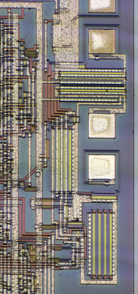
The circuit parts can be easily recognized due to the large structures.
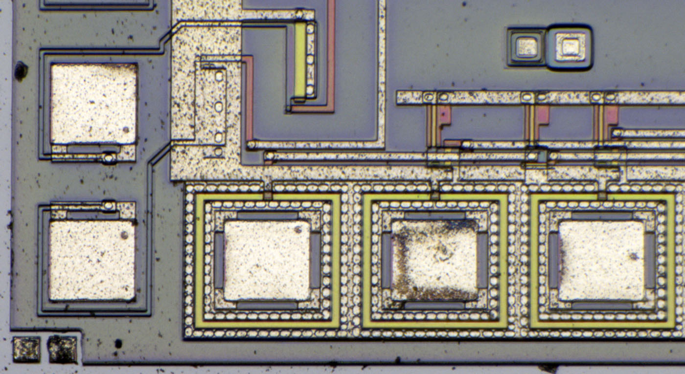
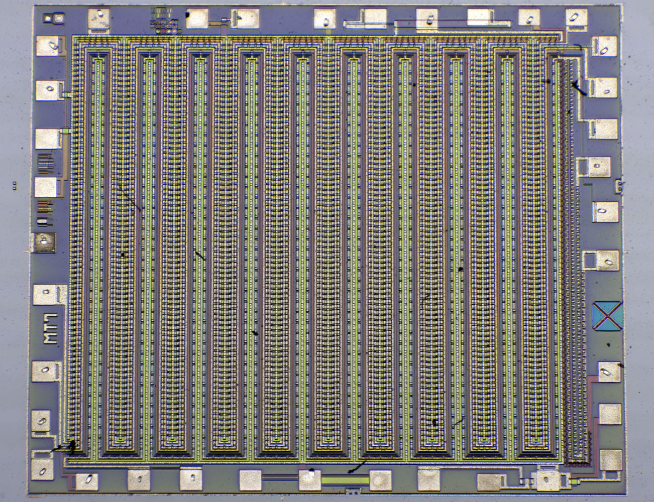
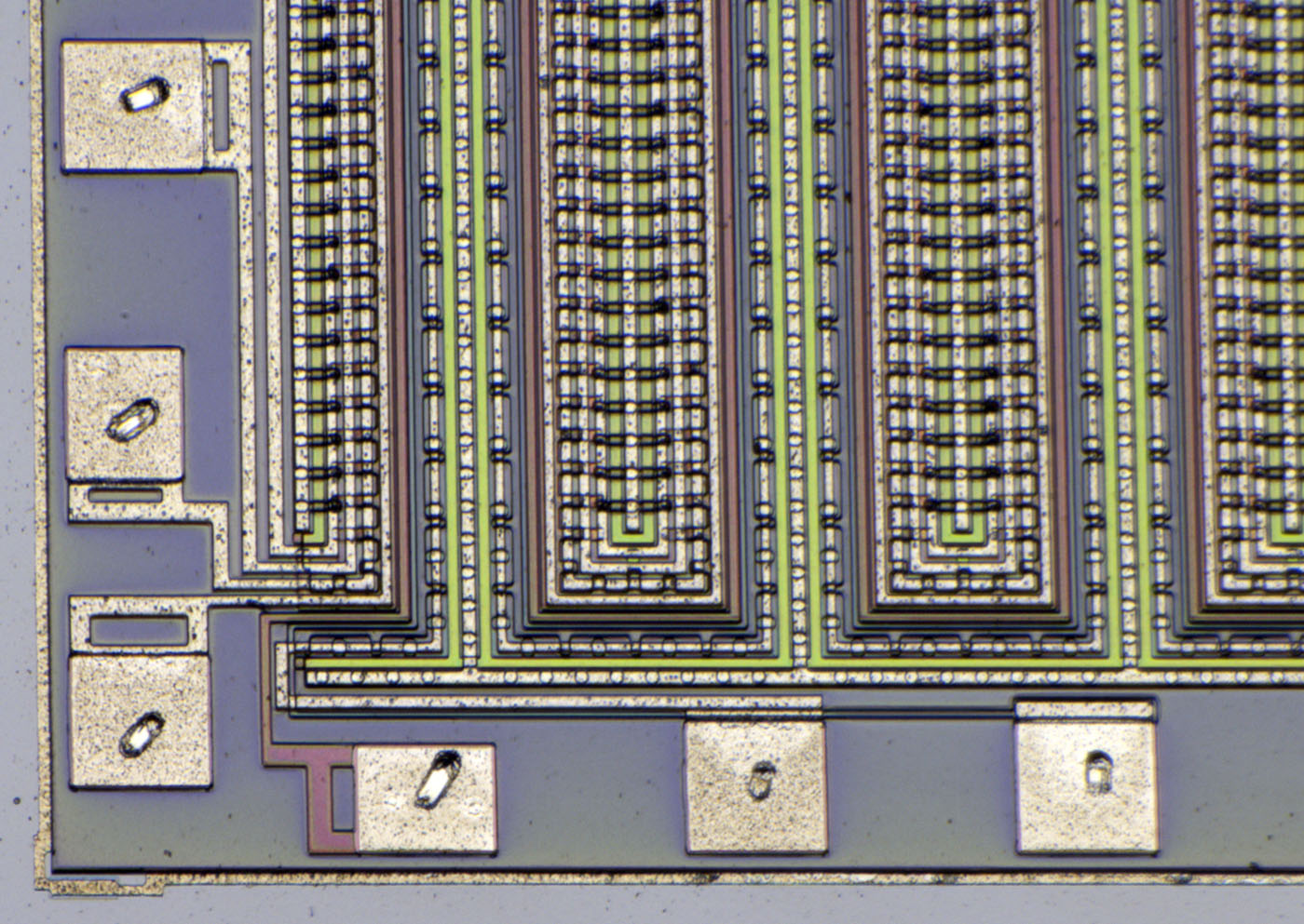
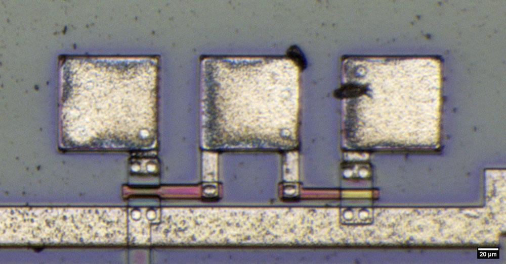
The Semiconductor Symposium document explains that the U809M has a total of 30 open-drain outputs with a common source connection. The implementation of these output stages is very unusual. One has built the transistor directly around the bondpad. The green appearing gate electrode separates the potential of the bondpad from the frame which carries the common source potential. Integrated above the output stages are the elongated transistors connected as pull-down resistors. Between the pull-down structures and the output stages, somewhat hidden, are the driver transistors that can pull the gate of the output stage transistors to a high level.
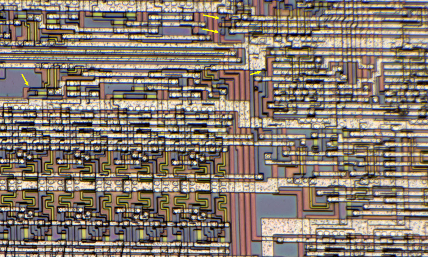
In addition to the outputs, the U809M has 13 inputs, two of which can be seen here on the left edge. A long thin line leads from the bondpad to a protection structure. The line serves as a current limiting resistor in case the protection structure becomes conductive. A slightly larger transistor serves as protection against positive voltages. Finally, it is a PMOS logic which is supplied with 0V (bulk) and -13V (Vdd). If the voltage at an input rises to positive values, the protection structure becomes conductive and limits the voltage. It could be that the structure is also protective at negative voltage peaks and thus is the complementary equivalent to the so-called "Grounded Gate NMOS".
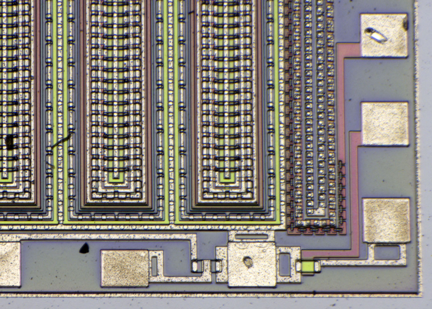
On the right edge there is a circuit whose structures clearly deviate from the rest of the logic structures. This is the RC oscillator (bottom), which outputs two complementary clock signals via two bondpads (top).
[...]


