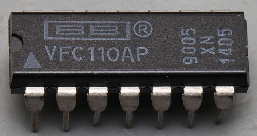
Burr-Brown VFC110, a voltage to frequency converter.
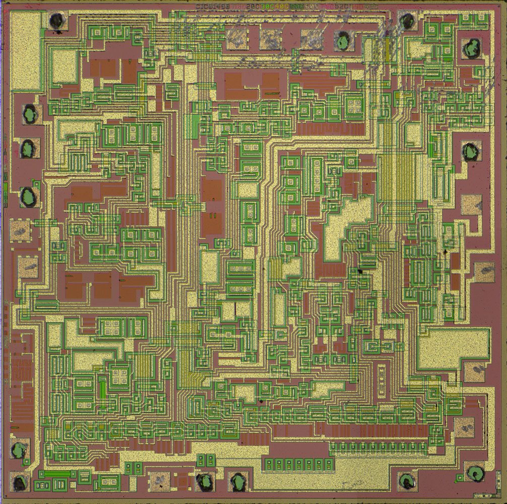
The edge length is 3,1mm.

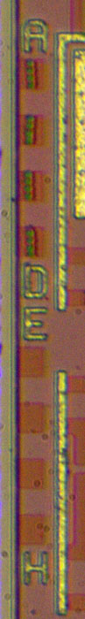
CIC01498, a typical Burr-Brown naming.
And some masks revisions.
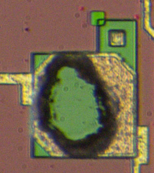
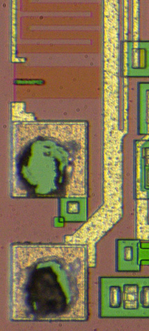
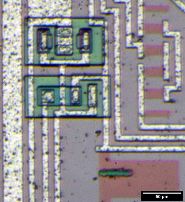
It looks like the eight squares were used to mark the tuning process...

At some bondpads there are interesting small squares. Probably protection...
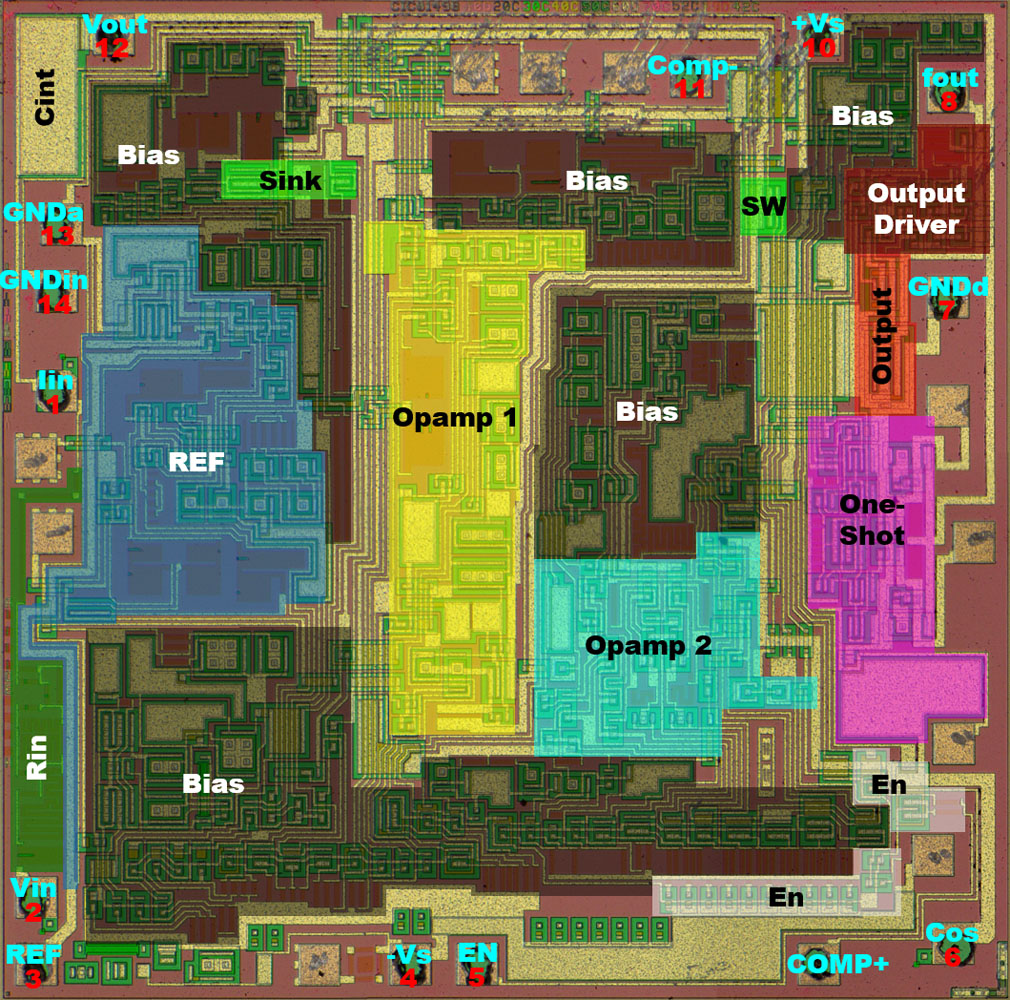
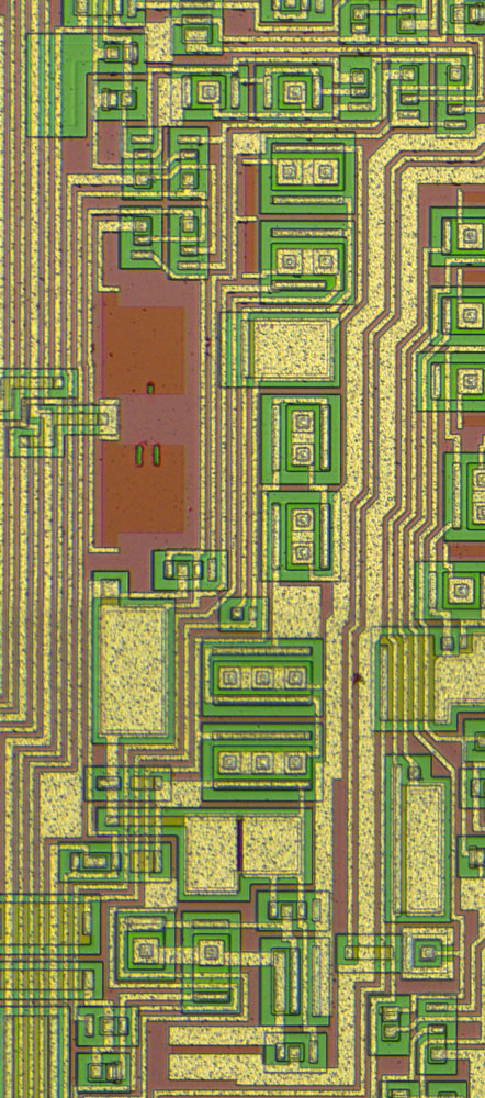
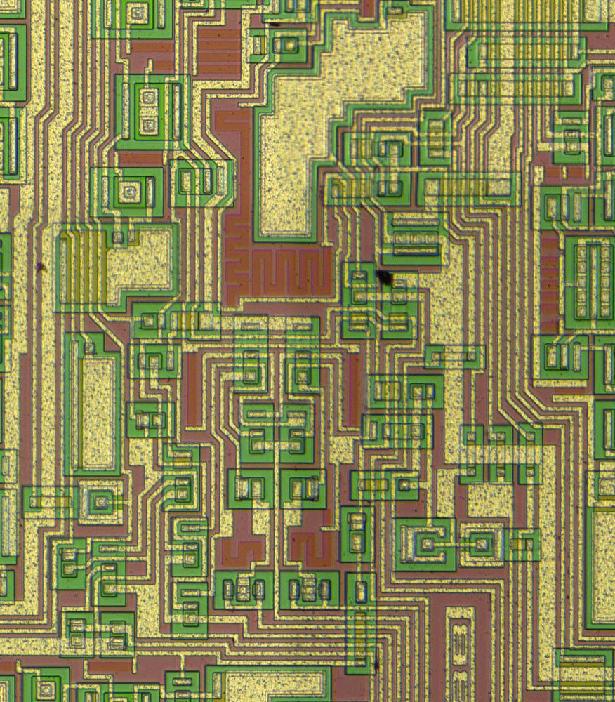
I´m not 100% sure but most functional blocks are easy to spot. Quite a lot of bias circuits.
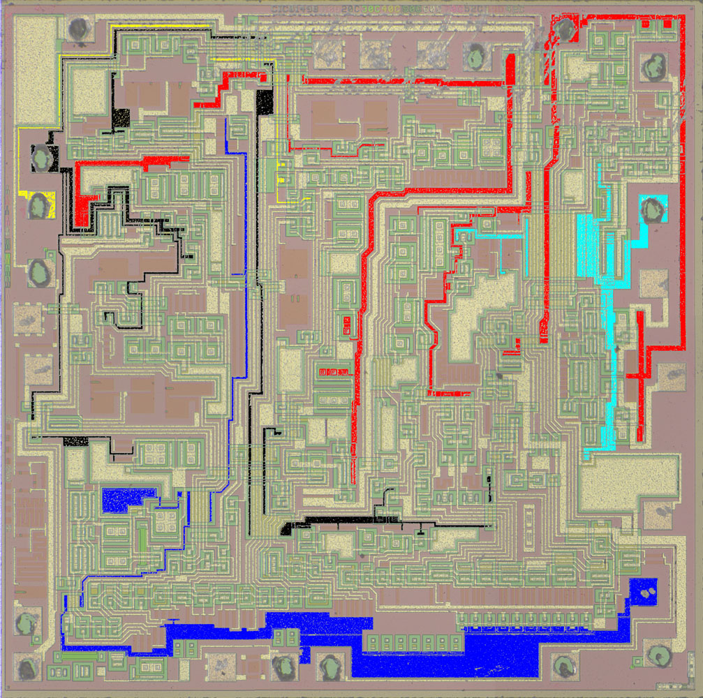
One metal layer and a lot of supply potentials.
Now that are a lot of current sinks.
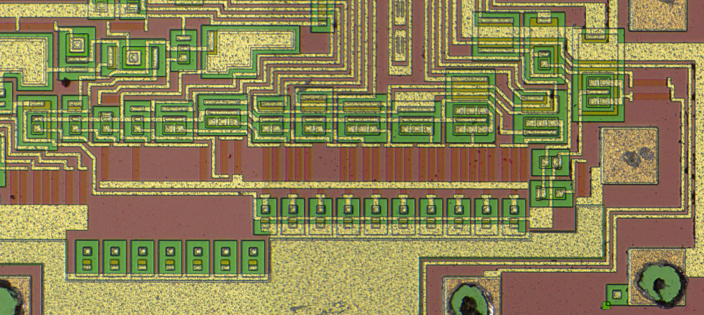
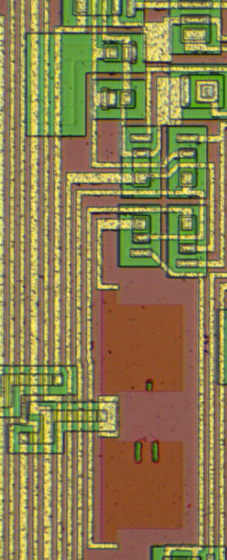
And a lot of the current sinks can be switched off with the enable pin.
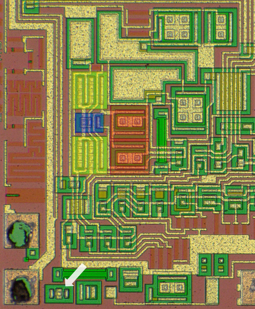
For the bias circuit BB integrated a bandgap reference.
There is also an unused buried zener. Interesting... Perhaps they thought about using the zener for the bias circuit.
The reference voltage circuit.
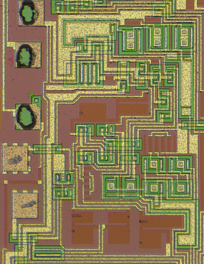
At the top of the area is the output with overcurrent protection.
We have cross coupled transistor quads and dummy resistors.
The reference voltage output uses a sense line to compensate for the voltage drop.
And here is the buried zener.
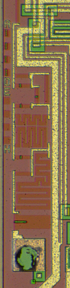
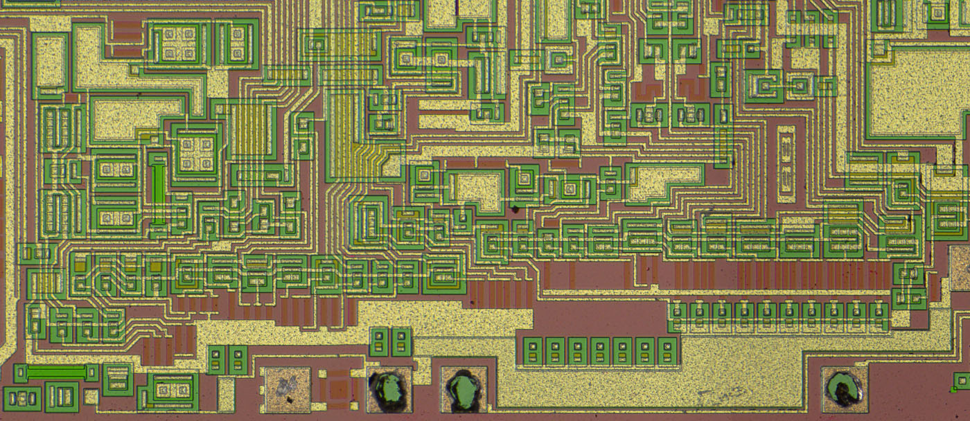
The input resistor is extensively tuned.
The first opamp, the integrator.
The opamp has diodes at the inputs. They prevent saturation and protect the input stage which is connected to the I_in pin.
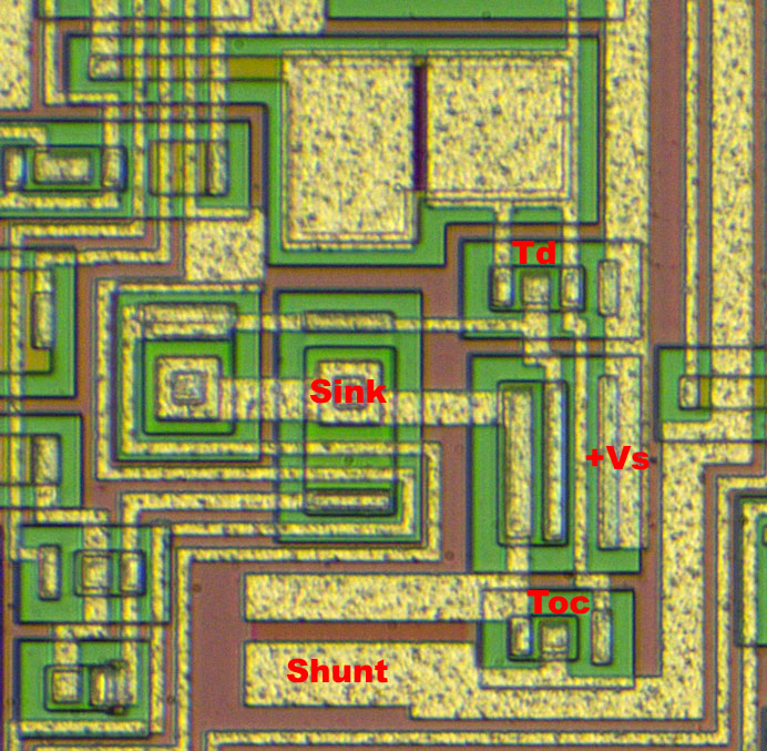
The output is connected to the V_out pin and because of that it contains a "power transistor" and an overcurrent protection like in the reference circuit.
The second opamp is quite symmetrical.
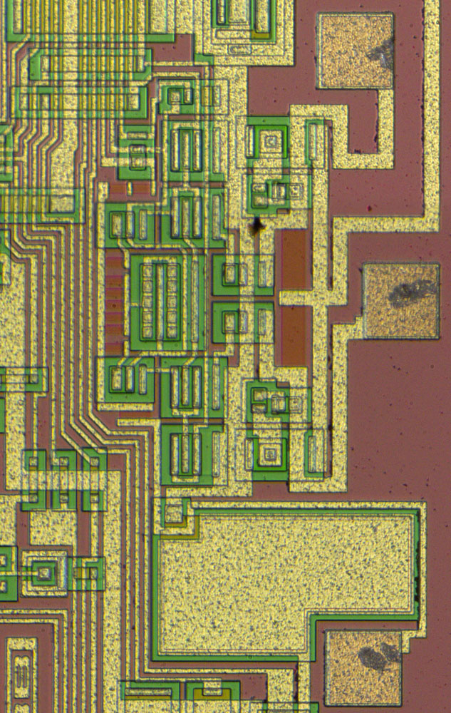
The one-shot-circuit which controls the pulse width.
Below the circuit there is the internal Cos-capacitor. You can connect an additional external capacitor.
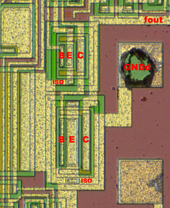
The output transistor is quite interesting. Around the active area there is an additional isolation frame ("iso") connected to GNDd. I assume the fast switching otherwise would causes a current flowing through the substrate to -Vs at the lower edge which could cause dirstubances in the other circuits.
More pictures here:
https://www.richis-lab.de/vfc01.htm 


