It seems that I have to create a DAC-topic.

Let´s start with the Burr Brown DAC709!
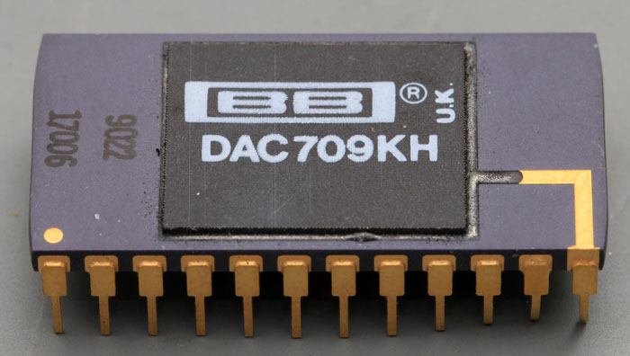
"U.K."

The datasheet gives you a lot of specifications:
Linearity Error: +/- 0,0015 %
Differential Linearity Error: +/- 0,003 %
Gain Error: +/- 0,07 %
Zero Error: +/- 0,05 %
Power Supply Sensitivity Vcc: +/- 0,0015 %/%Vcc
Power Supply Sensitivity Vdd: +/- 0,0001 %/%Vdd
Total Error Over Temp Range: +/- 0,08 %
Total Full Scale Drift: +/- 10 ppm/°C
Gain Drift: +/- 10 ppm/°C
Zero Drift: +/- 2,5 ppm/°C
Differential Linearity Drift: max + 0,009 / - 0,006 %
Linearity Error: max +/- 0,006 %
Settling Time (to +/-0,003%; voltage output): 4 µs
Slew Rate: 10 V/µs
Settling Time (to +/-0,003%; current output in 10Ω to 100Ω): 350 ns
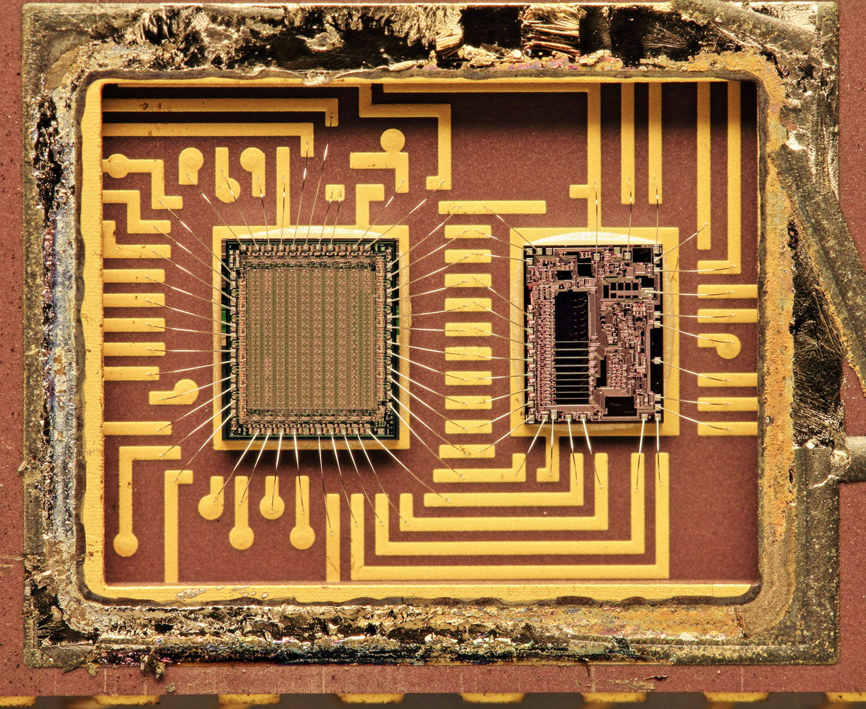
BB used two dies so they didn´t have to integrate the logic on the same die as the analog part which probably would have degraded the performance of the analog part.
BTW: The Package has two interconnection layers.
I think BB was able to configure the logic die so it acts as a DAC707, a DAC708 or a DAC709.
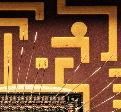
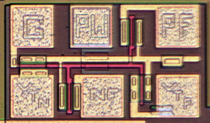
The two bondwires connected over an isolated square are promising candidates.
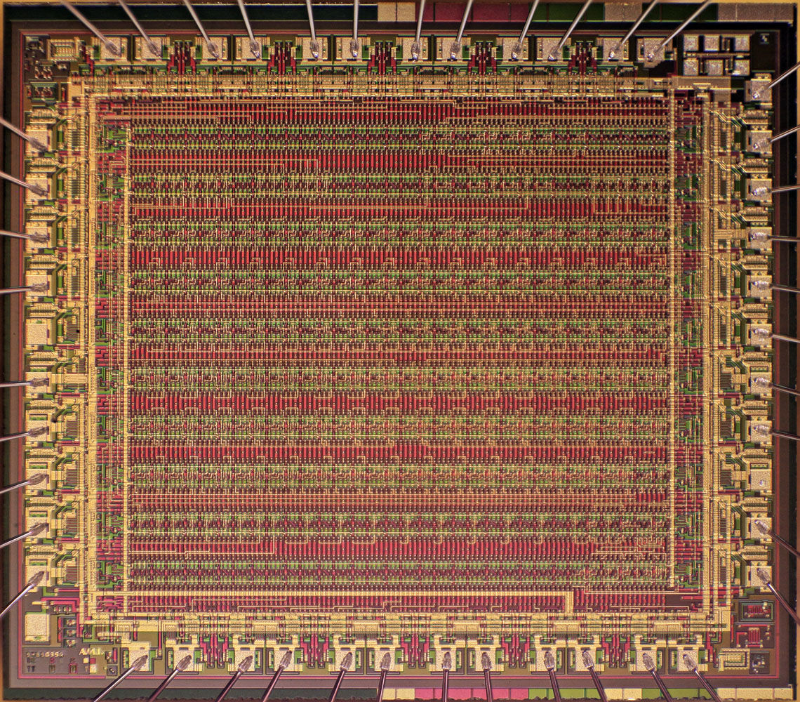
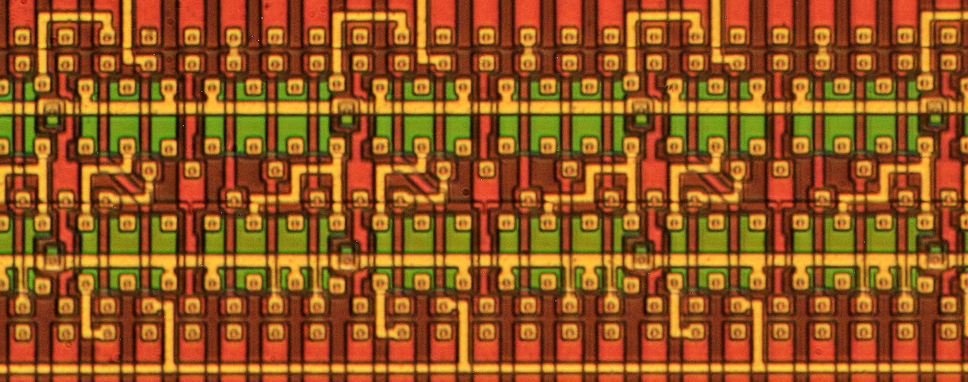
That´s an big old gatearray!

Nice test structures!
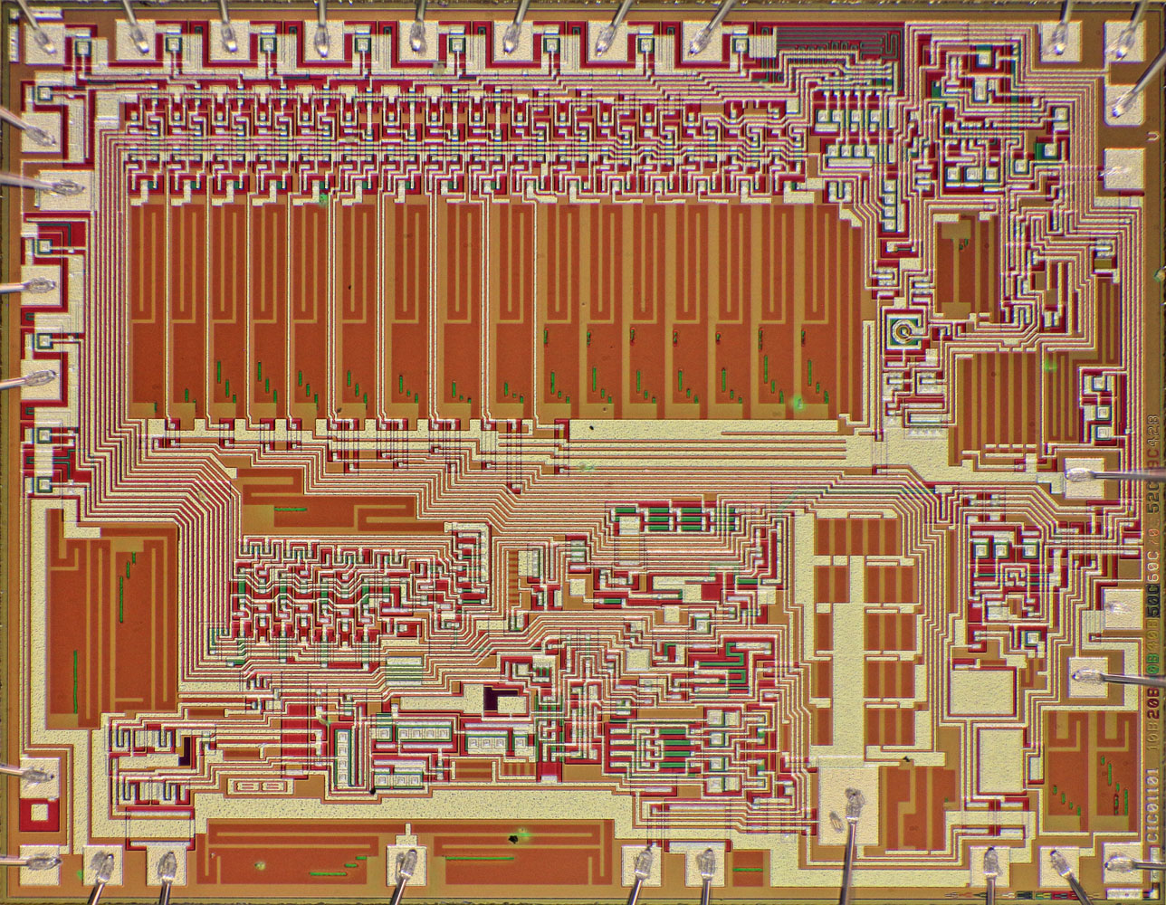
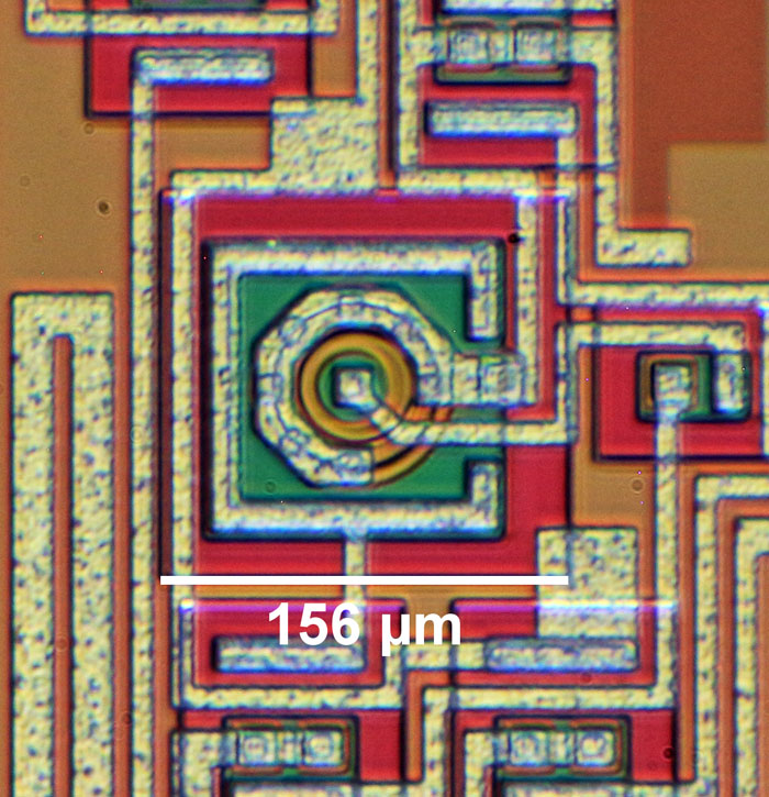
The DAC itself.
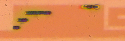
Resistor, Laser, Resistor, Laser, Resistor, Laser,...
Buried zener! Yeah!
Some more pictures here:
https://richis-lab.de/DAC01.htm


