Author Topic: DACs - die pictures  (Read 27222 times)

0 Members and 1 Guest are viewing this topic.

Offline NoopyTopic starter

  • Super Contributor
  • ***
  • Posts: 1812
  • Country: de
    • Richis-Lab
Re: DACs - die pictures
« Reply #75 on: September 21, 2020, 09:30:18 pm »
Today I have some DAC800 pictures for you:

https://richis-lab.de/DAC12.htm


Burr-Brown took two dies, a DAC and a Opamp.
Between the dies and the pin contacts BB used gold wire (bond-wedge) between the dies BB used aluminium wire (wedge-wedge).


Both dies are placed on a second die. I assume these additional dies reduce leakage currents. For the opamp that´s not necessary but with a additional die the opamp bonpads have the same height and it´s easier to bond wires.


The opamp is a OP-02, revision S built 1980.


The die is 2,74mm x 2,34mm.
The DAC800 doesn´t use a reference current path. It looks like there is a amplifier steering the current sink transistors.
Bit 1-3 are directly connected to the summing junction Bit 4-12 are scaled down with a R2R network.
Bits 1 and 2 have switches the switch the current to ground. The currents of Bit 3-12 are absorbed by the digital input circuits connected directly to the current sink transistors.


Buried zener...


But what´s that? They integrated two more buried zener in the bottom left and right corner! They are not connected to the circuits... For testing the buried zener structure one would have been enough...  :-//


I have also updated the DAC80 to some extend:

https://richis-lab.de/DAC02.htm


I first stated that this is a buried zener because in the newer datasheets the DAC80 is described as a DAC with a buried zener. But the older datasheets don´t mention a buried zener and the structure doesn´t look very special. Today I don´t think the DAC80 reference voltage is based on a buried zener.

 :-/O

Offline NoopyTopic starter

  • Super Contributor
  • ***
  • Posts: 1812
  • Country: de
    • Richis-Lab
Re: DACs - die pictures
« Reply #76 on: September 29, 2020, 08:30:51 pm »
Hi all!

Today I have a more modern DAC for you, a DAC8564 with four 16Bit-DACs:


It provides no 16Bit accuracy. The "relative" accuracy is +/-4LSB between 485 and 64714. The offset is +/-5mV.
The maximum power consumption is below 10mW!  :-+


The die is coated but a small window was left open.


You can see the two double DACs left and right on the die.


Designed 2007.


Hm, what is that? There are structures in the "windows". That´s no capacitor! Is that the 50MHz digital input interface with a massive metal screen for less disturbances?


Under the window in the coating there is a big steady structure. I assume that´s a memory block. Are these small rectangles testpoints? Perhaps they did some alignment and to do so they had to contact the memory directly.


Perhaps the part in the middle of the die contains the reference. Perhaps not...  ;D


Now that´s one of the double-DACs!
You can see the logic area in the middle.
In my view the big rectangle contains the resistor string mentioned in the datasheet.
Perhaps the smaller rectangles are smaller DACs to aligne the big ones. Often big resistor strings are aligned with the help of smaller resistor strings that generate reference potentials for the big ones. Well we can´t be sure about the smaller rectangles but the big one has interesting connections at the top and at the bottom. Perhaps these are reference points?


Every output uses two bondpads. You can see there are two lines connecting the bondpads, a small and a bigger one. I´m pretty sure the big one is the output of the opamp arranged right (and left) of the DAC. There is also a uniform square, could be a capacitor for compensation of the opamp...


More pictures here:
https://richis-lab.de/DAC13.htm


 :popcorn:
 
The following users thanked this post: exe

Offline exe

  • Supporter
  • ****
  • Posts: 2590
  • Country: nl
  • self-educated hobbyist
Re: DACs - die pictures
« Reply #77 on: September 30, 2020, 07:14:36 pm »
Fantastic! I was skeptical that they had four independent dac channels. I suspected they used some sort of multiplexing and I'm glad I was wrong.

DAC specs are not stellar, but it's hard to find something precise, cheap, and with 3 or 4 channels. I guess some of the error comes from the opamps. I wish there was a cheap current-output dac (or even just a "multiplying" dac). But those seem to target precision gear and are expensive.
 

Offline NoopyTopic starter

  • Super Contributor
  • ***
  • Posts: 1812
  • Country: de
    • Richis-Lab
Re: DACs - die pictures
« Reply #78 on: September 30, 2020, 07:53:47 pm »
Well the DAC8564 is not bad at all!
Four independent DACs in such a small package, 50MHz serial input, <10mW power consumption (!), a integrated reference. That´s not bad.  :-+

16Bit accuracy is even today not easy to achieve.
With 0,5mA the LSB gives us 7nA. With 3V the LSB gives us 45µV.
Even if the DAC can resolve 16Bit you have to build a circuit that´s able to handle that small voltages good enough.  :-/O
 
The following users thanked this post: exe

Offline NoopyTopic starter

  • Super Contributor
  • ***
  • Posts: 1812
  • Country: de
    • Richis-Lab
Re: DACs - die pictures
« Reply #79 on: September 30, 2020, 09:21:55 pm »
Taking a look at the AD1139 (https://www.richis-lab.de/DAC07.htm) I found a 12/14Bit-DAC without a marking. I presumed that it is a AD7535 and of course I had to take a closer look at a AD7535:

https://www.richis-lab.de/DAC14.htm

I was right!  8) ;D


Offline NoopyTopic starter

  • Super Contributor
  • ***
  • Posts: 1812
  • Country: de
    • Richis-Lab
Re: DACs - die pictures
« Reply #80 on: October 02, 2020, 10:00:45 pm »
I just thought about the trimmed resistors of the AD7535:


Only the first resistor was adjusted but every resistor has such wide areas to make laser trimming possible.
Perhaps the better grade of the AD7535 is not generated by sorting the parts but by trimming more resistors...

Offline tkamiya

  • Super Contributor
  • ***
  • Posts: 2178
  • Country: us
Re: DACs - die pictures
« Reply #81 on: October 03, 2020, 10:02:00 pm »
What's so nice about Noopy's work is that everything is in FULL COLOR, and very vibrant.  A lot of previous work by others I've seen are nothing like these.  I'm so surprised reversed macro lens can resolve this much.

I have a question though.  Some of the images are captured in 3D fashion.  Do you stack images?  Surely, you don't have enough of DOF to do this all by itself.
 

Offline NoopyTopic starter

  • Super Contributor
  • ***
  • Posts: 1812
  • Country: de
    • Richis-Lab
Re: DACs - die pictures
« Reply #82 on: October 04, 2020, 03:29:34 am »
Thanks!
I had to invest a lot of time to get there.  :-/O

Sometimes I get better pictures with a small tilt. Of course I then have to do focus stacking.
The tilted pictures are ofte very nice to look at but I try to avoid them because the geometries are... ...tilted... You get a little less height. You know what I mean?


It´s not very much but it´s there...

...and the tilted pictures take a lot of time and memory (33 pictures taking 845MB in this case)...  ;D

Online mawyatt

  • Super Contributor
  • ***
  • Posts: 3445
  • Country: us
Re: DACs - die pictures
« Reply #83 on: October 04, 2020, 07:21:48 pm »

The tilted pictures are ofte very nice to look at but I try to avoid them because the geometries are... ...tilted... You get a little less height. You know what I mean?


This is where you want to investigate "Telecentric Lens". Many pages of discussions from ~2006 on these lenses on the PM site. If you ever get involved with Stack & Stitch images like we have (producing Gigapixel chip images) you will appreciate these type of lenses where apparent magnification doesn't depend on subject to lens distance ;)


http://www.photomacrography.net/forum/viewtopic.php?t=1418

https://www.photomacrography.net/forum/viewtopic.php?f=8&t=1472&hilit=Telecentric

https://www.photomacrography.net/forum/viewtopic.php?f=8&t=1032&p=5541&hilit=Telecentric#p5541

Best,
Curiosity killed the cat, also depleted my wallet!
~Wyatt Labs by Mike~
 
The following users thanked this post: Noopy

Offline NoopyTopic starter

  • Super Contributor
  • ***
  • Posts: 1812
  • Country: de
    • Richis-Lab
Re: DACs - die pictures
« Reply #84 on: October 04, 2020, 08:02:30 pm »
I have learned a lot about optics but it seems I still have to learn more.  ;D
Thanks for the links.  :-+ It will take some time to read and understand everything...  :-/O

Online mawyatt

  • Super Contributor
  • ***
  • Posts: 3445
  • Country: us
Re: DACs - die pictures
« Reply #85 on: October 04, 2020, 08:43:52 pm »
Fun stuff indeed :)

What's really interesting is that with a stacked lens setup (one lens reversed stacked upon another longer lens) by placing a simple paper aperture of the correct size and placement convents this lens combo into a telecentric result. With the right combination this can produce a very good overall lenses system without significant cost.

One of the features not often mentioned with the benchmark Mitutoyo inf corrected objective lenses, is they are almost telecentric and one reason they produce nice focus stacking results.

Best,
Curiosity killed the cat, also depleted my wallet!
~Wyatt Labs by Mike~
 

Offline NoopyTopic starter

  • Super Contributor
  • ***
  • Posts: 1812
  • Country: de
    • Richis-Lab
Re: DACs - die pictures
« Reply #86 on: October 04, 2020, 08:56:39 pm »
Indeed very interesting!

Two lenses, that always sounds like worse pictures. In my view at some magnification more glass gives only less resolution. But perhaps I´m wrong...  :-/O

Online mawyatt

  • Super Contributor
  • ***
  • Posts: 3445
  • Country: us
Re: DACs - die pictures
« Reply #87 on: October 04, 2020, 09:47:15 pm »
Don't think of it as two separate lens, but additional optical elements added to create a new overall lens. Almost all modern lens are made up of multiple elements, some of the latest have upwards of 20 elements!! So adding more glass may not always be a bad thing ;)

Best,
Curiosity killed the cat, also depleted my wallet!
~Wyatt Labs by Mike~
 

Offline NoopyTopic starter

  • Super Contributor
  • ***
  • Posts: 1812
  • Country: de
    • Richis-Lab
Re: DACs - die pictures
« Reply #88 on: October 17, 2020, 08:21:46 pm »
I have taken pictures of an old DAC80:
https://www.richis-lab.de/DAC02.htm
A lot of dies, just a simple zener as reference.

I also have taken pictures of a DAC800:
https://www.richis-lab.de/DAC12.htm
Burr-Brown was able to integrate everything on one die except the output opamp.
The zener reference is treated to get better performance.


And now I have pictures of a DAC811:


Now everything is on one die and Burr-Brown also integrated three 4Bit- and one 12Bit-latch.


The DAC and the reference in the DAC800 is the same as in the DAC811 (bottom).


Here you can see the output opamp.


Ten masks with a revision A. No optimization necesary? Sounds strange...


Let´s take a look into an older DAC811.


There is something like silicone on the die but not over the whole area. Perhaps the silicone just had to protect the tuned resistors....


You can find some small differences but nothing special.


The masks on this die were optimized more than once: two times "J"!  :o
And Burr-Brown gave the design even another name! Interesting...


More pictures here:

https://www.richis-lab.de/DAC15.htm

 
The following users thanked this post: doktor pyta

Offline NoopyTopic starter

  • Super Contributor
  • ***
  • Posts: 1812
  • Country: de
    • Richis-Lab
Re: DACs - die pictures
« Reply #89 on: November 04, 2020, 12:03:27 pm »
Let´s take a look into a AD7111, a logarithmic 17Bit-DAC:


The AD7111 gives you the posibility to control a 88,5dB-attenuation with 0,375dB steps. In fact the accuracy is way of 17Bit but that´s no bigger problem in audio applications for example.


The die is 3,7mm x 2,7mm.


There is a p-channel MOSFET and a n-channel MOSFET test structure. JR and BH probably are initials of the engineers.


The DAC is based on a R2R-ladder.
Between each resistors there is a "dummy resistor" connected to ground. I assume that should reduce leackage currents. There is also a Vdd shielding in the upper area.
Under the resistors there are the switch transistors. Only the first two have different areas for equal current density.


The diagonal structure is the decoder generating the logarithmic steps.


The digital input buffer is placed as isolated rectangles near the bondpads.


https://www.richis-lab.de/DAC16.htm

 :-/O
« Last Edit: November 04, 2020, 12:21:15 pm by Noopy »
 
The following users thanked this post: exe, Miyuki

Offline NoopyTopic starter

  • Super Contributor
  • ***
  • Posts: 1812
  • Country: de
    • Richis-Lab
Re: DACs - die pictures
« Reply #90 on: November 10, 2020, 01:36:50 pm »
Let´s take a look into a latvian DAC: ALFA 572ПA1А - 572PA1A


There is some potting on the die (and some dirt caused by the decapping).  :-/O


The die is 2,45mm x 1,95mm. You can easily spot the different areas. In the middle there are the R2R resistors. At every digital input there are the control circuits and the current switch transistors for the R2R-ladder. The areas of the current switch transistors are halfed jumping from the MSB to the lower Bits. Bits 6 to 10 all have the same small transistor because their errors don´t contribute very much to the overall error budget.


Hey, there are two more Bits not connected (current switch transistors are shorted). In the R2R-ladder there are some spare resistors which could be used to generate two more Bits. Perhaps there was a similar DAC with 12Bit resolution.

The datasheet shows a swith off circuit which connects the R2R-ladder to ground and is controlled by the supply voltage. But you can´t find this circuit on the die. Perhaps the circuit was integrated later (datasheet dates back to 2016 vs. date code 1983).


More pictures here:
https://www.richis-lab.de/DAC17.htm

 :-/O

Offline NoopyTopic starter

  • Super Contributor
  • ***
  • Posts: 1812
  • Country: de
    • Richis-Lab
Re: DACs - die pictures
« Reply #91 on: December 17, 2020, 12:18:26 pm »

Offline NoopyTopic starter

  • Super Contributor
  • ***
  • Posts: 1812
  • Country: de
    • Richis-Lab
Re: DACs - die pictures
« Reply #92 on: January 14, 2021, 08:59:37 pm »
Today I have some DAC800 pictures for you:

https://richis-lab.de/DAC12.htm


...


Now let´s look into a DAC800P (epoxy package):


As in the DAC800 there are two dies. But here we have only one metal plate supplying the dies with the negative supply. In the DAC800 the substrate of the DAC, the substrate of the opamp, the DAC circuit and the opamp circuit have their own contact (leading to the -Vcc pin).


The DAC in the DAC800 and the DAC in the DAC800P share the same design revision.
It looks like BB used two different bondwires as we have seen in the DAC800 (ball- and wedge-bond).


And also the same opamp...


https://www.richis-lab.de/DAC12.htm

 :-/O
 
The following users thanked this post: SeanB, macboy, zarcondeegrissom, serg-el, 3g57

Offline NoopyTopic starter

  • Super Contributor
  • ***
  • Posts: 1812
  • Country: de
    • Richis-Lab
Re: DACs - die pictures
« Reply #93 on: August 13, 2021, 04:37:24 am »
Warning: this topic has not been posted in for at least 120 days.  :o
We need more DACs!  ;D


Hybrid Systems DAC327 gives you 16Bit over a wide temperature range: -25°C - 85°C
I found a first ad dating back to 1978.  :-+


It´s a metal package with a welded lid.


The datasheet contains a block diagram.
There was a DAC327 with a 10V reference and one without it. Here we have the one without the reference.
There was also a BCD version. This one has a binary interface.


The DAC327 is quite similar to the Burr-Brown DAC80 (https://www.richis-lab.de/DAC02.htm).
There are four ICL8018 switchable current sinks with resistor networks and two resistor networks dividing the currents by 16.
OP1 is the output opamp, OP2 generates the reference current with the ICL8018 1x4.
You can see the place where the reference can be placed. It looks like there is room for a reference zener and an opamp.
There is also a free area for a BCD circuit. It has to realize the overdrive function that gives you up to 12V in BCD mode. Would be interesting to see how this is done.


We already know the ICL8018 but...


...these ICL8018 don´t look good. It seems like there was some kind of corrosion or a manufacturing problem.  :o


The resistor network of the MSB ICL8018. Four resistors are for the four current sinks and one is for the reference current.
The smallest resistor is tuned a lot. There is one area for bigger changes (cutting to get the resistor longer) and one area for smaller changes (cutting to get the resistor thinner).
R is the resistor which has to be most accurate.


The "lower" resistor arrays don´t need the fifth resistor and are less tuned.


Probably a laser process?!


Here you can see the two 1/16 divider arrays, tuned of course.
It´s interesting how bad the edges of the dies look like. You could have seen that at the ICL8018 resistor arrays but these arrays look really bad, splintered and burnt.  :o


The output opamp, nothing special.
Is someone able to identify the model and manufacturer?


A nice compensation capacitor.


The opamp for the reference current generation, nothing special.
Is someone able to identify the model and manufacturer?


Some more resistors for the output feedback and the current generation.


Look at the upper resistor, what a crazy tuning!  :o


https://www.richis-lab.de/DAC18.htm

 :-/O
 
The following users thanked this post: SeanB, RoGeorge, zarcondeegrissom

Offline magic

  • Super Contributor
  • ***
  • Posts: 6888
  • Country: pl
Re: DACs - die pictures
« Reply #94 on: August 13, 2021, 04:47:14 am »
...these ICL8018 don´t look good. It seems like there was some kind of corrosion or a manufacturing problem.  :o
The spots on the second one look like what happens when I try to wash something with IPA or acetone and leave the solvent on the die to dry.
The first one is quite dirty or  :-//

The opamp for the reference current generation, nothing special.
Is someone able to identify the model and manufacturer?
2×NPN and 2×PNP in the input stage, that's gonna be some 741/101 kind of thing. Both of them.

edit
The first one connects the input NPNs to VCC through a diode. This artificially limits its common mode input range to less than VCC which means it was marketed as "xx741" despite the use of LM101A input stage. There were millions of those 101A/741 hybrids with CMIR-limited 101A input stage, 741-compatible offset trimming, various kinds of VAS / output stage and various overcurrent limit schemes. I suppose you could try to catalog them all when you get bored of 555 timers ;D

One example schematic of such hybrid can be found in the current Texas Instruments OP07 datasheet, don't ask me why :-DD

The second one has no such diode and the input range includes VCC. There is internal compensation and no offset trim. These features point to LM107 or equivalent and the schematic seems to check out, including somewhat atypical compensation.

Your first opamp is photographed upside down. Negative at the top, positive at the bottom. All the electrons will surely fall out ;)
« Last Edit: August 13, 2021, 10:08:23 am by magic »
 
The following users thanked this post: Noopy

Offline NoopyTopic starter

  • Super Contributor
  • ***
  • Posts: 1812
  • Country: de
    • Richis-Lab
Re: DACs - die pictures
« Reply #95 on: August 13, 2021, 04:04:04 pm »
...these ICL8018 don´t look good. It seems like there was some kind of corrosion or a manufacturing problem.  :o
The spots on the second one look like what happens when I try to wash something with IPA or acetone and leave the solvent on the die to dry.
The first one is quite dirty or  :-//

There should be no dirt caused by my decapping.  :-//


Your first opamp is photographed upside down. Negative at the top, positive at the bottom. All the electrons will surely fall out ;)

Oh no!  :wtf: ;D
 
The following users thanked this post: zarcondeegrissom

Offline David Hess

  • Super Contributor
  • ***
  • Posts: 16844
  • Country: us
  • DavidH
Re: DACs - die pictures
« Reply #96 on: August 14, 2021, 04:11:01 am »
I seem to have only seen BB used in military electronics and avionics so far. If those were their target markets, or their biggest consumers, then cost may have been only a secondary concern.

BB also made a lot of consumer stuff. I believe they were big in the audio sector. Made some good audio-oriented low distortion opamps, ADCs and DACs. Bought by TI in 2000.

Burr-Brown ended up doing a lot of high end audio ADCs, DACs, and operational amplifiers.  My guess is that it was a natural progression for them from the precision market once people started using their precision parts for high end audio anyway.

Burr-Brown was definitely a "premium" supplier like Precision Monolithic Incorporated and Linear Technology which were both bought by Analog Devices, and all three wrote excellent datasheets and application notes.  Of those three, Burr-Brown was definitely the heaviest into the military and aerospace markets.  PMI and LT also played the premium audio game.

Both dies are placed on a second die. I assume these additional dies reduce leakage currents. For the opamp that´s not necessary but with a additional die the opamp bonpads have the same height and it´s easier to bond wires.

In precision parts, they might stack dies to reduce stress in the precision part.  This is also why analog parts use a different package encapsulation than digital parts.
 
The following users thanked this post: Noopy

Online mawyatt

  • Super Contributor
  • ***
  • Posts: 3445
  • Country: us
Re: DACs - die pictures
« Reply #97 on: August 14, 2021, 01:05:26 pm »
Agree, BB was an excellent source of precision analog devices back in the 70~80s, we used a BB 18bit hybrid DAC back in late 70s. An interesting side note on BB (also ComLinear), the high performance bipolar chips they offered were not fabricated in-house. They used a complementary bipolar process developed at Bell Labs in Reading, PA, which later became known as CBIC-V2. Even Harris used this process over their in-house UHF bonded wafer process.

Best,
Curiosity killed the cat, also depleted my wallet!
~Wyatt Labs by Mike~
 

Offline NoopyTopic starter

  • Super Contributor
  • ***
  • Posts: 1812
  • Country: de
    • Richis-Lab
Re: DACs - die pictures
« Reply #98 on: July 06, 2022, 10:43:15 am »


The AD562 is a 12bit DAC built by Analog Devices. The device was advertised as new in EDN magazine in 1974. The cheapest grade was $58 at the time, which would be equivalent to $344 today (2022). The best grade is advertised at $150. Converted to today's purchasing power (2022) that is $889.

Depending on the grade the accuracy of the AD562 is +/-0,25LSB (25°C). The operating temperature range starts at -55°C and ends at +125°C. Temperature coefficients are a maximum of 4ppm/°C for offset and 5ppm/°C for gain (referring to full scale). Settling time is typically 1,5µs and is a significant point that was optimized in the successor AD565 (https://www.richis-lab.de/DAC06.htm). Parallel to the AD562 there was a AD563 which contained an additional voltage reference.


The package contains a die with an edge length of 4,5mm. The ground pin on the right edge has been triple contacted to reduce interfering voltage drops.


The magazine EDN (Volume 20, Number 2, 20.1.1975) contains an article about the AD562 which shows and describes that originally two elements were integrated into the case. In this version the resistors were had their own die.


In "Analog-Digital Conversion Notes" from Analog Devices (August 1980) there is a block diagram that shows the DAC split into two parts. In the upper part the active elements are integrated and in the lower part there are the resistors which get laser tuned.


The original layout of the AD562 is still clearly visible on the fully integrated die.


The numbers 562 can be assigned to the component designation. The meaning of the letter E and the single number 8 remain open.

The test structure above the component designation contains a pinch resistor and an NPN transistor.


In many of the resistors you can see a marking due to the laser tuning. At the upper resistor you can see that the laser started quite a bit outside the resistor area.

The number 1 in the isolated square probably makes it possible to trace the alignment process one way or another.


The "Data-Acquisition Databook 1982" from Analog Devices contains a simplified schematic of the AD562.


The schematic in the "Analog-Digital Conversion Notes" from Analog Devices is a little more detailed.

An operational amplifier controls with an external voltage reference a reference current sink, which consumes 500µA. The opamp at the same time drives the other current sinks which sink 1mA, 500µA, 250µA and 125µA. The currents are set by the emitter resistors. The transistors are of different sizes so that the current density remains the same and the transistors behave as equally as possible.

The switching threshold of the digital interface can be switched between TTL and CMOS by pin 2. Finally change-over switches are controlled which connect the current sinks with the ground potential or the output.

The current sinks consist of three groups of four with 1mA, 500µA, 250µA and 125µA each. To be able to display the smaller current values, there are current dividers, so-called "interquad dividers", between the groups. The output current can thus be varied between 0mA and 2mA. The structure of the smallest current sinks is slightly different from the larger ones. More about this later.

The two 5kΩ resistors at the output allow to set an output voltage range of 10V or 20V. The 9.95kΩ resistor is used to create a bipolar output voltage. It is not a 10kΩ resistor so that external adjustment is possible with a 100Ω potentiometer. For the same reason the resistor at the input of the reference current opamp is just 19.95kΩ.


The individual areas can be easily identified on the die. At the upper edge the digital signals are processed (cyan). The switching threshold is delivered from a circuit in the left area (pink).

In the left area there is also the opamp (yellow), which controls the reference current sink. The area ratios 8:4:2:1 of the current sink transistors (dark gray/light gray) are clearly visible. In contrast, the third group has a ratio of 4:2:1:0,5.

Between the digital interface and the current sinks are the changeover switches which connect the current sinks to the output (dark green) or terminate them via the ground potential (red). Here different sizes can be seen too. However the area ratios do not quite match the current ratios, especially for the lower bits. Here the ratio is less critical because the current value is still divided by 16 respectively by 128 and the error is reduced accordingly. In general, the current densities of the switchers have a smaller influence on the total error of the DAC.

In the middle of the current sinking transistors there is a small circuit (light green) which generates a bias potential for the changeover switches. The bias potential defines at the same time the potential at the collectors of the current sinks.


The emitter resistors of the current sinks are located directly under the associated transistors (dark gray / light gray). In the first group the areas are larger than in the second. The resistor values are the same but the larger areas make the tuning easier. Errors are most critical in the first group since it supplies the largest part of the output current. The third group on the other hand could be constructed more simple.

At the right edge of the die are the two current dividers (blue). At the lower edge there are thr resistors for setting the output voltage range (purple). On the left side the input resistors of the reference current opamp are integrated (yellow).


[...]
 
The following users thanked this post: SeanB, D Straney, mawyatt

Offline NoopyTopic starter

  • Super Contributor
  • ***
  • Posts: 1812
  • Country: de
    • Richis-Lab
Re: DACs - die pictures
« Reply #99 on: July 06, 2022, 10:44:23 am »


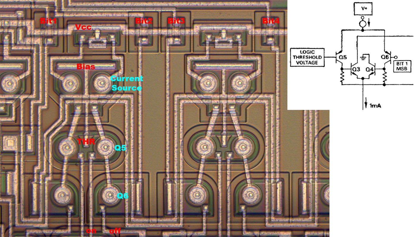
The "Analog-Digital Conversion Notes" show how the digital input signals are processed. It is a differential amplifier built with PNP transistors whose two outputs control the two transistors of the current switch. On one side of the differential amplifier (Q6) the input signal is applied, the potential on the other side (Q5) defines the switching threshold.

On the die the PNP differential amplifiers are arranged in pairs. The top transistor represents the current source. It is controlled from the left side of the die. Below it is the transistor Q5 of the differential amplifier. The current sources and the transistors Q5 use the same base potentials for all inputs, which is why it was possible to integrate them in pairs in the same base area and save silicon area. The second transistor of the differential amplifier (Q6), on the other hand, has an exclusive base area. The two control signals "on" and "off" at the bottom are the output signals.


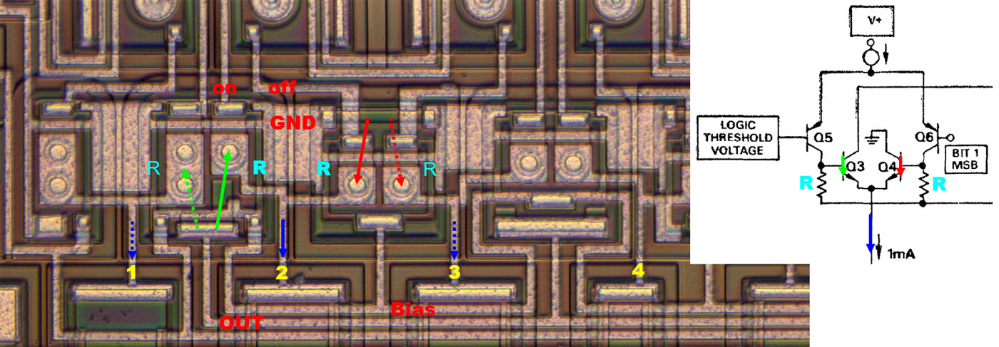
The four switching transistors of adjacent current sinks (yellow/blue) were combined in pairs. Two transistors leading to the output (green) alternate with two transistors neutralizing the current via the ground potential (red). The collector resistors of the controlling transistors (cyan) work against a bias potential.


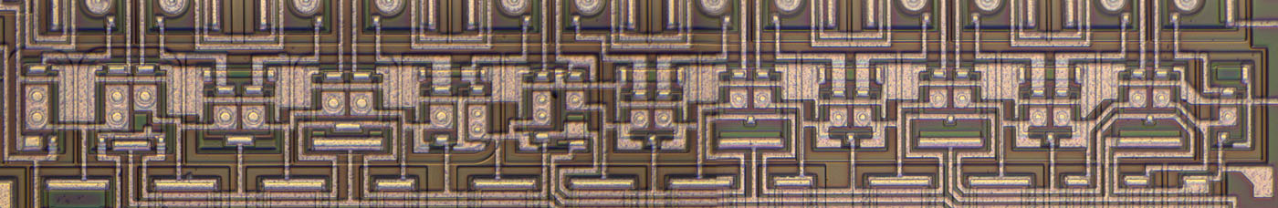
The routing of the signals over the whole width of the current sinks and changeover switches is not unproblematic with just one metal layer.


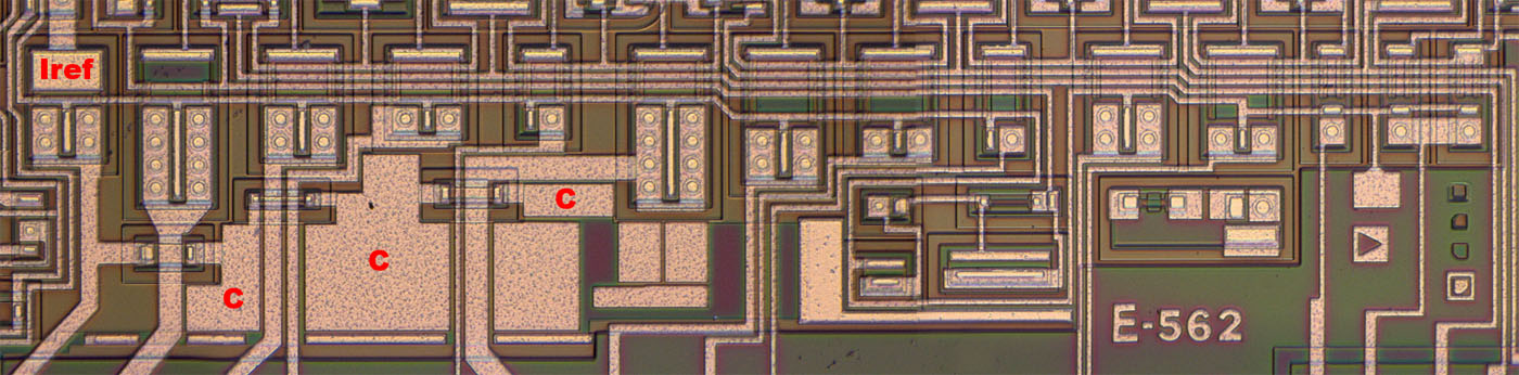
There are some capacitor plates connected to the emitter potential of the transistor that sets the reference current. This probably improves the control loop behaviour. The isolated metal surfaces could be reservations to be able to increase this capacity with a small change of the metal layer.


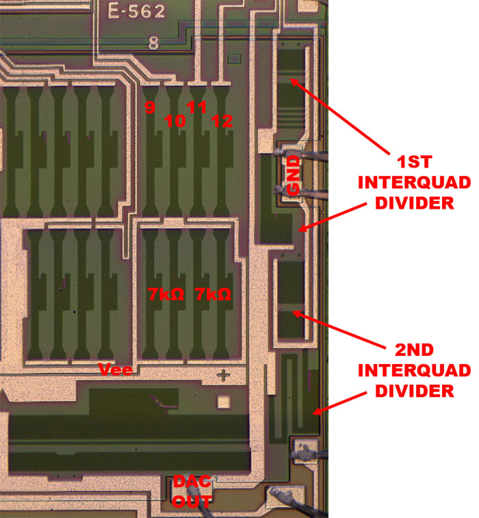
The footpoints of the current sinks are combined in a star configuration as far as possible. This is important so that the current sinks do not disturb each other and can all work with the same reference potential. The negative supply is routed from the bondpad to these resistors over an exclusive line. The upper part of the AD562 is connected via a separate line.

The farther to the left the resistors are in the current sink row, the greater their influence on the overall error of the DAC. For this reason, the large resistors and the first small resistors are surrounded by dummy structures at the edges. They are not visible at first glance because the metal layer hides them. The dummy structures ensure that the resistors at the edges behave as much as possible like the internal ones. This way manufacturing processes have a more uniform effect on the relevant surfaces due to the more homogeneous environment.


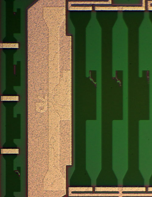
If you vary focus and exposure time the dummy structures become more prominent. On the far left, there is an additional symbol that cannot be interpreted.  :-//


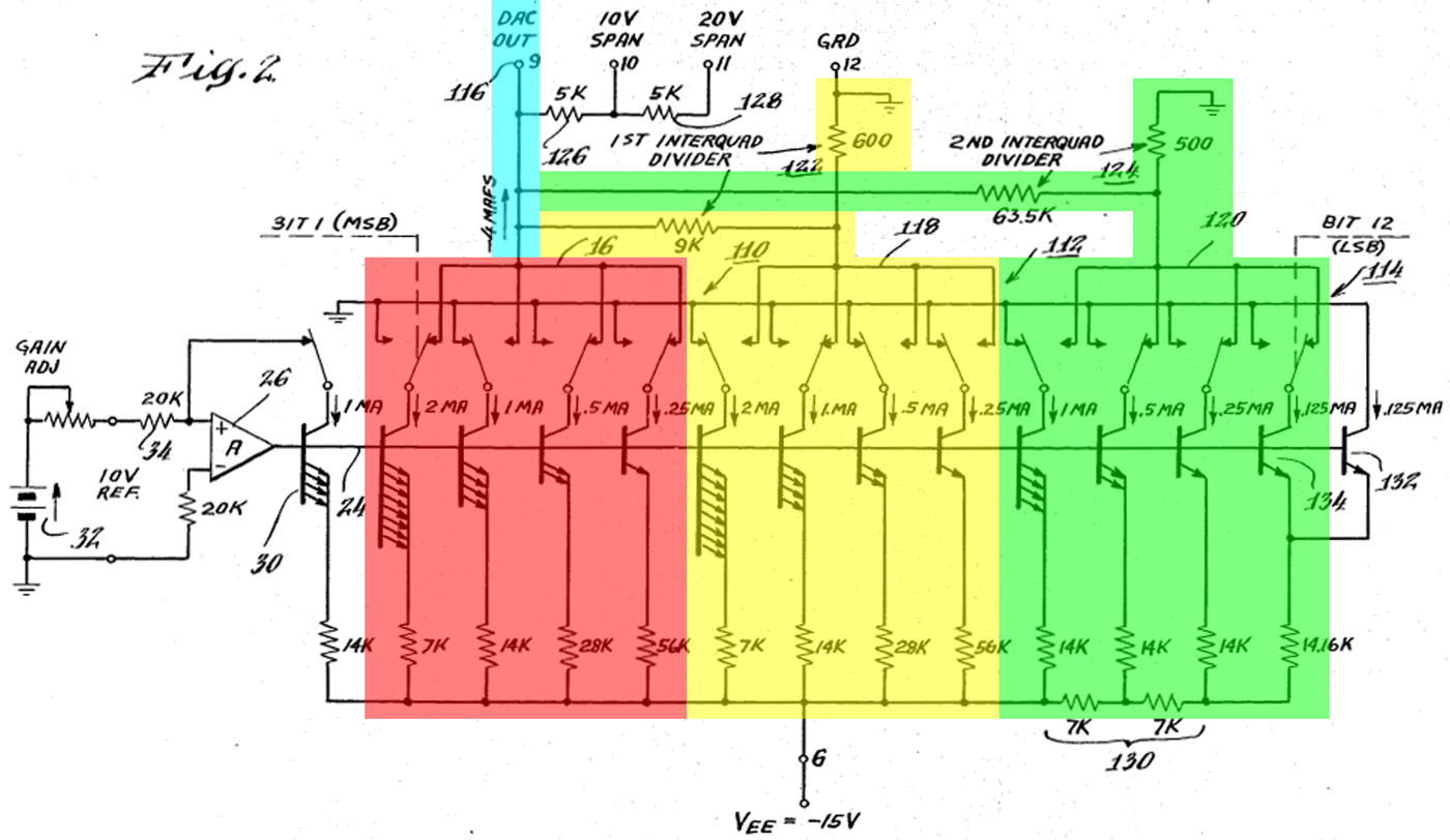
The datasheet of the AD562 refers among other things to the patent US3961326. In this patent the structure of the DAC is shown in more detail. The circuit diagram has been colored for better understanding. The currents are entered incorrectly. With a 10V reference voltage and the 20kΩ resistor the opamp sets a reference current of 500µA, as shown in the schematics above. The remaining currents have to be halved accordingly.

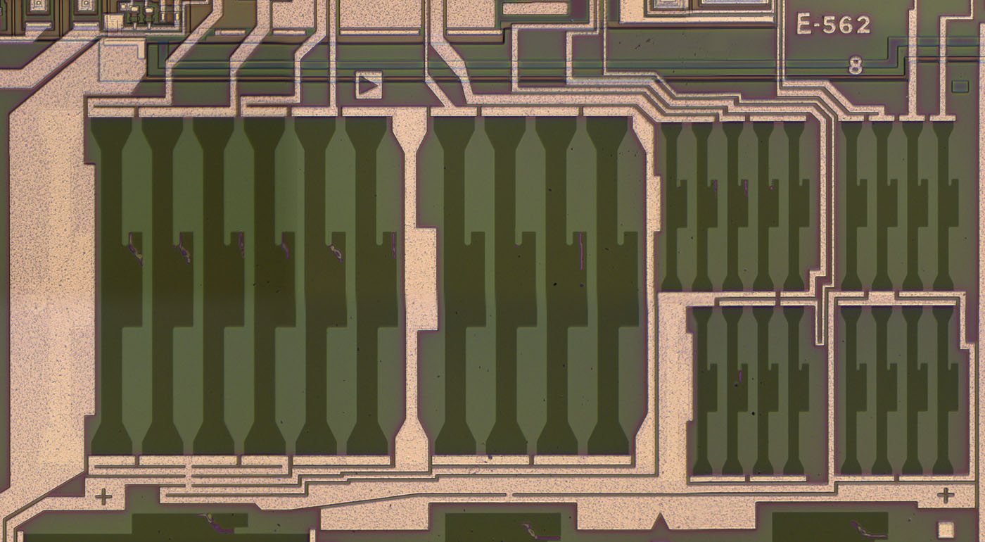
The first group (red) contains four current sinks. Related to the reference current generation, the resistance ratio is 0.5:1:2:4. This provides a current ratio of 2:1:0.5:0.25 or in absolute values 1mA, 500µA, 250µA, 125µA. These current sinks are connected to the output (cyan) depending on the digital input signal.

The second group of current sinks (yellow) has the same structure as the first group. However the output current passes through an "interquad divider", a current divider that reduces the currents by a factor of 16. The exact resistor values differ a little from the resistor values in the documents above, but the factors are the same. The 1/16 current divider is just used by the second group. The third group (green) has its own current divider. Alternatively, one can also work with two 1/16 dividers connected in series as implemented in the DAC-HZ12 for example (https://www.richis-lab.de/DAC05.htm).

The third group of current sinks (green) has a slightly different structure in detail than the first two groups. Since the error contributions of the current sinks located further to the right have less effect on the output due to the current dividers, the third group can be implemented more simply, which means that the circuit takes up less area on the die. The strongest current sink of the third group takes just 500µA. This is the reason why the second current divider does not have a factor of 1/256 but a factor of 1/128. The first three current sinks of the third group have equal emitter resistances. In order to be able to generate a current ratio of 8:4:2, there are 7kΩ resistors between the current sinks. The sum currents of the following current sinks flow through these resistors. The smallest current sink operates with a 14kΩ emitter resistor too. The division of the current is represented by a second transistor (132) whose output is fixed to the ground potential. Transistors 134 and 132 share the current, which produces the desired current ratio. Finally, the sum current of the third group is connected to the output through the second current divider.


With the background of the patent US3961326 the wiring of the resistors in the AD562 can be understood much better.

The two current dividers on the right edge have an exclusive ground potential, which is connected to the case via two bond wires. Unlike many other currents at critical points in the DAC the currents in the current dividers change with the desired output current. These changes result in varying voltage drops, which in turn can negatively affect the quality of the output signal. For this reason, the currents are diverted through an exclusive lower-resistance path.

The lower resistors of the current dividers were tuned similarly to the resistors in the current sinks. The upper resistors additionally seem to offer the possibility of a very rough adjustment by cutting larger areas completely.


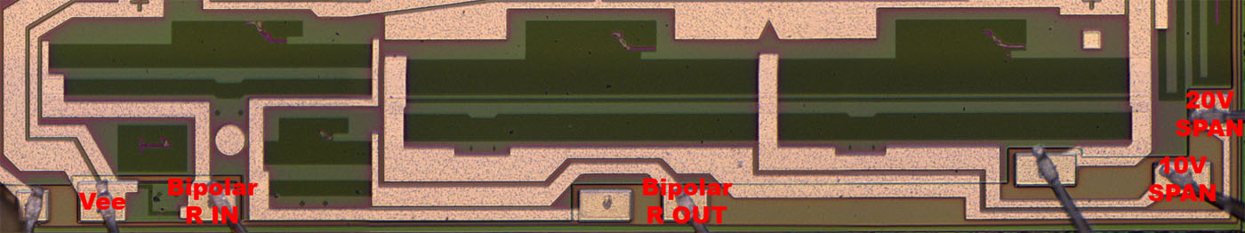
The resistors needed for the external conversion of the output current into a voltage are integrated at the lower edge of the die. This reduces the external part requirements. Since a trimming process is used in the AD562 anyway, it is also very cheap to generate exact resistor values.

Additional resistors are connected in parallel to the adjusted resistors. The notches with the two dots suggest that these resistors were intended for an adjustment too. The resistor for setting a bipolar output voltage consists of two elements. Between these elements is an additional bondpad, so that one can set a different resistor value by varying the bondwires.


The bondpad BIPOLAR OFFSET R IN has a connection to the negative supply which was cut during the tuning.


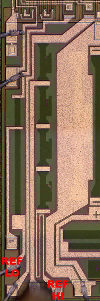
On the left edge of the die there are the two input resistors that lead to the opamp that sets the reference current. The resistor value critical for the reference current at the bondpad REF HI consists of four resistor elements, each of which can be adjusted individually.

Next to the bondpad REF HI there is a free bondpad which is hard to see in this picture. This bondpad makes it possible to contact only a quarter of the REF HI resistor. In the REF LO path there is a tap too. According to the location it gives you a quarter of the resistor too. The tap at a quarter seems to be absolutely logical with regard to the AD563. The AD563 has an additional 2.5V voltage reference. To be able to generate the same currents with the 2.5V the resistance at the input of the reference current control must be reduced to a quarter.


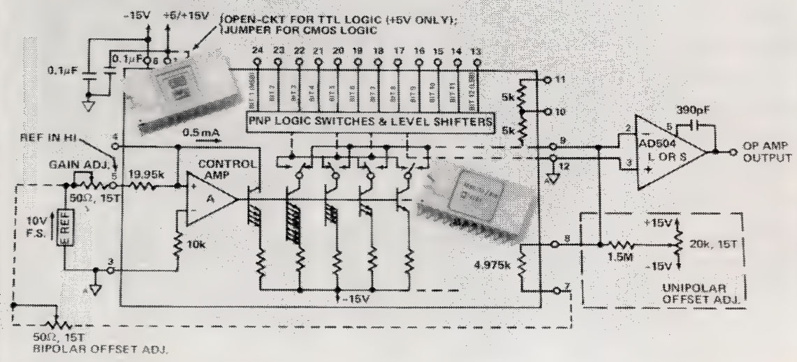
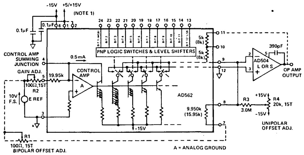
Looking at the schematic published in the magazine EDN (Volume 19, Number 20, 20.10.1974) (above) and the schematic in the "Data-Acquisition Databook 1982" by Analog Devices (below) very different resistors can be found.

According to the EDN magazine, there could be a resistor with a value of 10kΩ at the non-inverting input of the reference current opamp. At the same time, there would be a 20kΩ resistor at the inverting input. This does not seem logical since one usually tries to keep the resistors on both inputs of an opamp the same size so that the effects of the bias currents compensate each other as much as possible. In most documents both resistors are specified as 20kΩ. It is likely that the 10kΩ is a typographical error.

The two resistors for setting the output voltage range are usually specified as 5kΩ. In the "Data-Acquisition Databook 1982" 8kΩ is specified in parentheses as an alternative. This would explain the tapers and the markings on the resistors connected in parallel. Probably one can increase the resistor values to 8kΩ by cutting the parallel strings.

If one increases the 5kΩ feedback resistors one must adjust the resistor for bipolar operation too. In the "Data-Acquisition Databook 1982" this resistor value is accordingly additionally given with 16kΩ. This resistor too offers parallel connected resistors which can be cut. However one could probably alternatively use the center tap to represent the 5kΩ shown in the EDN magazine. In this configuration "bipolar operation" would result in an output current range of 0mA to 2mA, which does not seem particularly useful. The purpose of the alternative 5kΩ resistor is not obvious.  :-//

In the present AD562 there are once again other resistors: The resistance at the input of the reference current source can be determined with 22kΩ. The resistors for setting the output voltage range are 5,5kΩ each and the resistor for the bipolar operation offers 11kΩ fittingly.


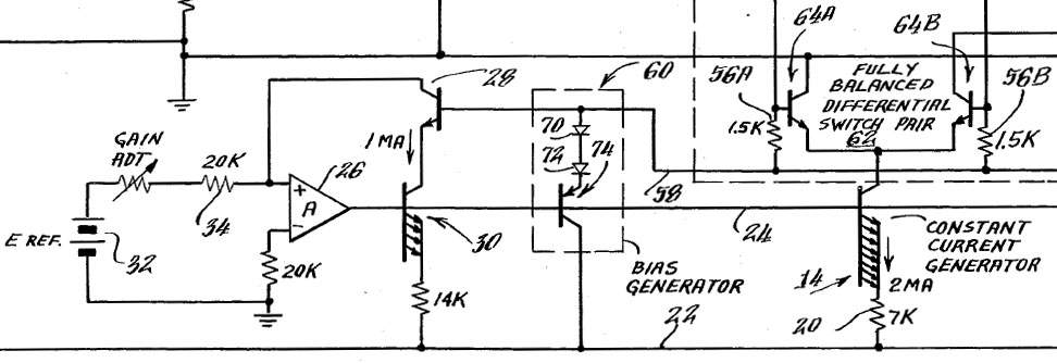
The circuit diagram in patent US3961326 shows the circuit part 60 which generates a bias voltage. This bias voltage ensures via the transistors of the changeover switches that the collector-base voltage of the current sinks remains constant.


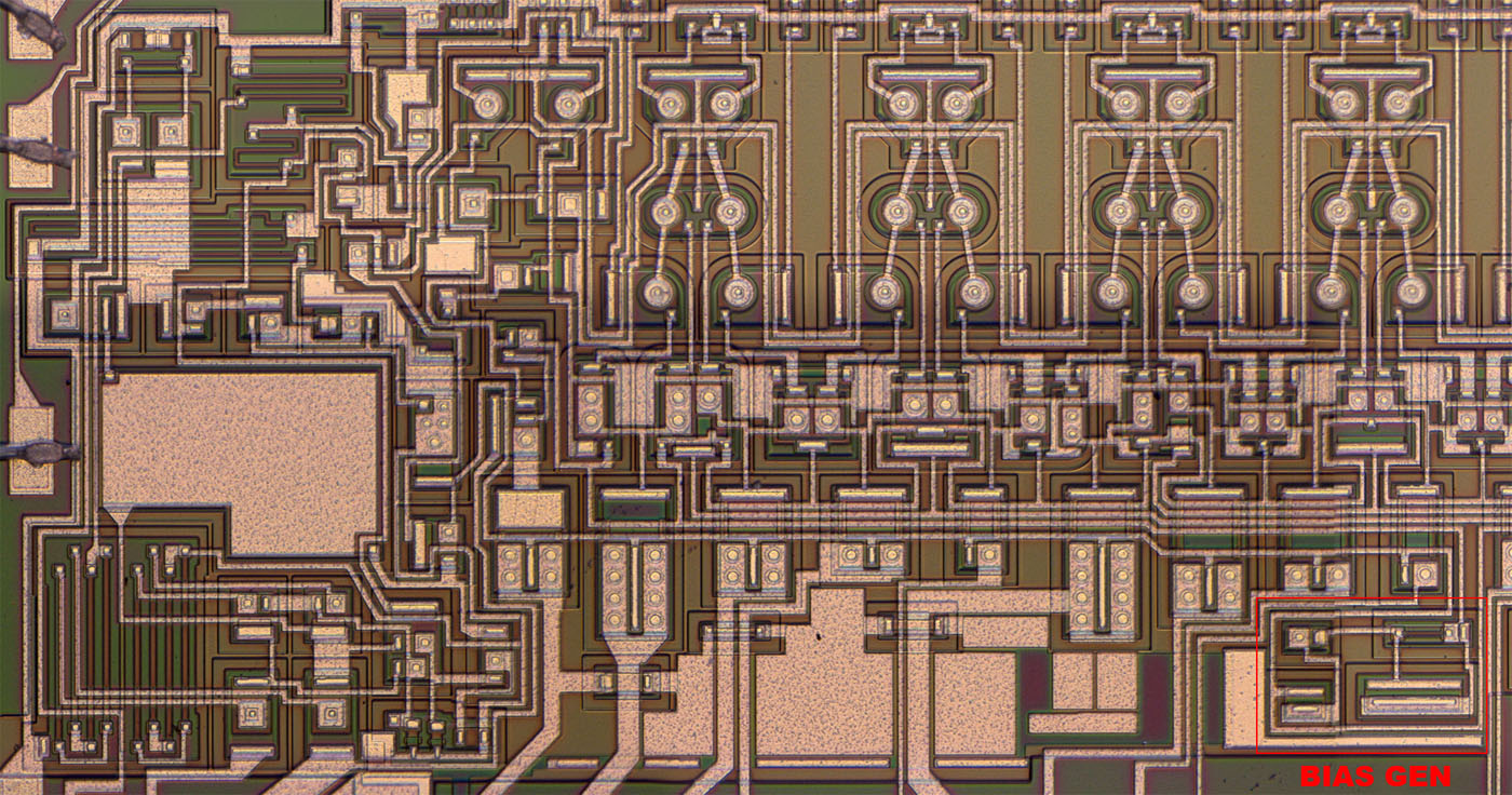
The elements that generate the bias voltage have been integrated into the center of the DAC. Presumably this was done to ensure that the circuit and the current sinks have the same temperature.


https://www.richis-lab.de/DAC19.htm

 :-/O
 
The following users thanked this post: SeanB


Share me

Digg  Facebook  SlashDot  Delicious  Technorati  Twitter  Google  Yahoo
Smf