Hi all,
I have took a closer look on a LM399 shunt reference.
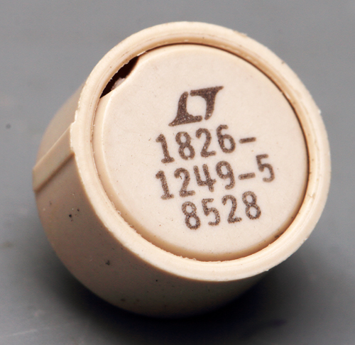
Actually it´s a HP-part...
You can find the whole story here:
https://www.richis-lab.de/REF02.htm(german)
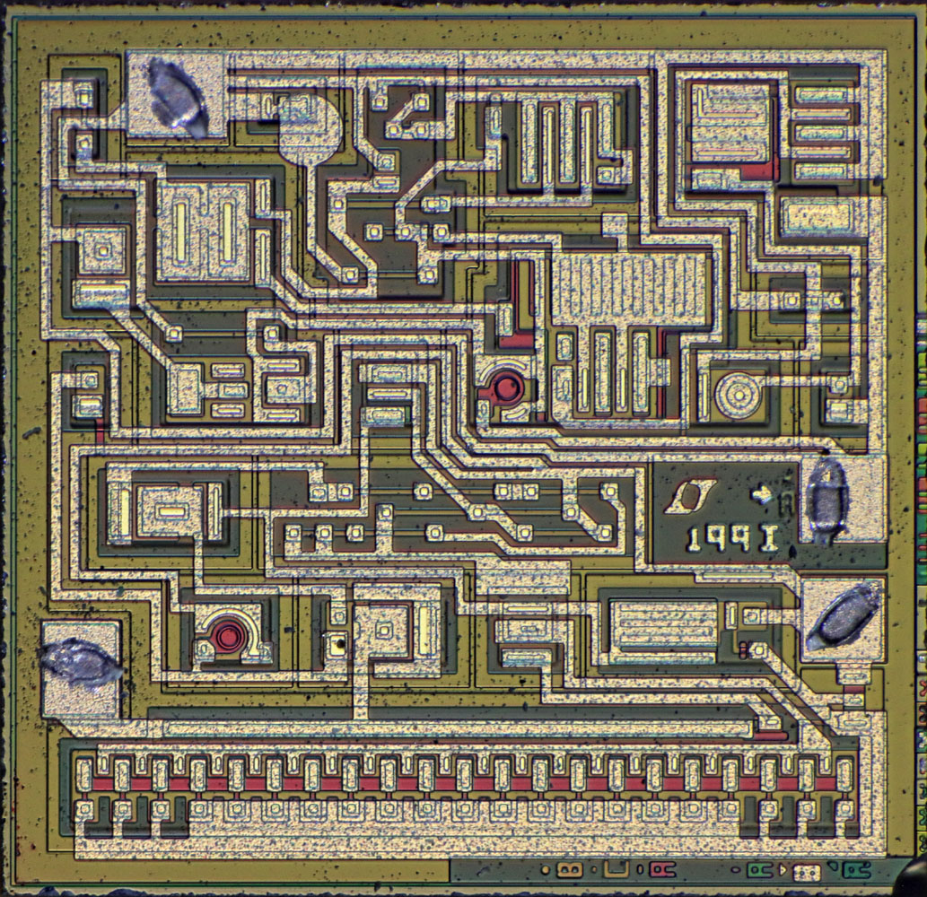
A nice die with big structures!

Reverse engineering is not a big deal:
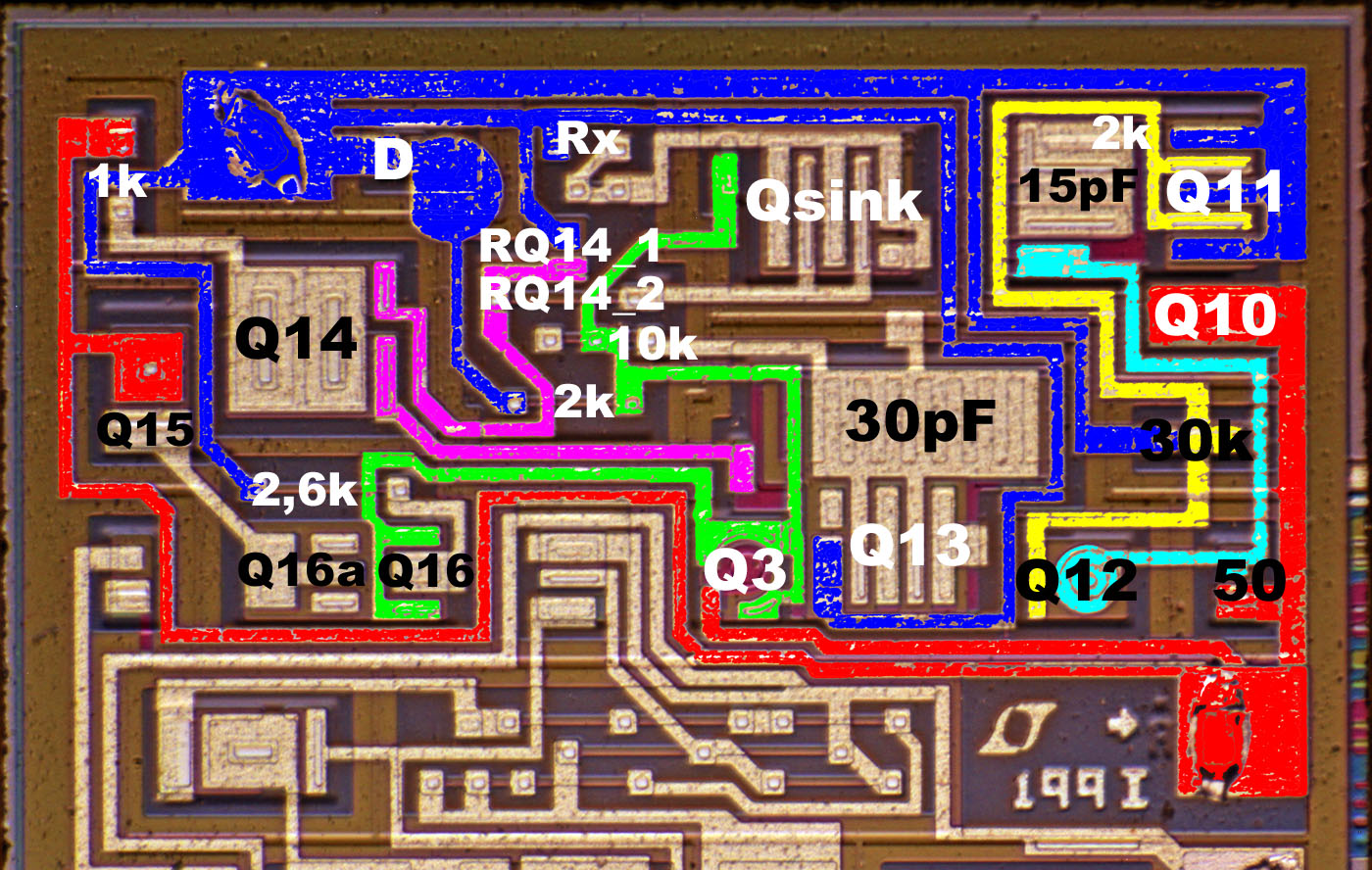
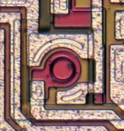
And here is the buried zener:
I found a circuit that´s not in the datasheet:
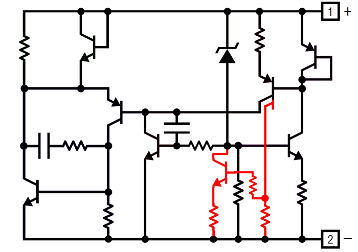
It seems they had to do some fancy compensation.

And here the heater-circuit:

I wrote a lot about the circuit but it´s too late to translate all that words to english. Please use the google translator and ask me whatever you want.

BTW:
I also have a PMI REF01:
https://www.richis-lab.de/REF01.htm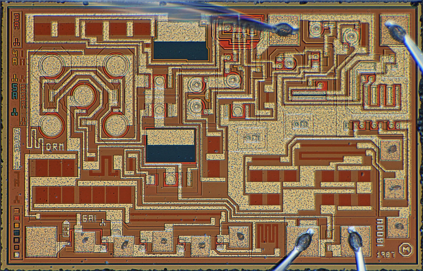
Interesting point: The new ones are ADR01 named REF01.
Have fun!
…does anybody want to donate me a (dead) LTZ1000?

Update: Hey, it seem´s that I´ll get one out of the german mikrocontroller.net-Forum!


