Are you afraid of the thick traces?

- Vdd comes out of the regulator, goes to C6, mcu, back to C8. Why? Put them in parallel in the same trace.
- Mcu Vdd pin goes to L1, L1 goes to C9 and C10 goes nowhere?
- VDDA goes to C11, but not connected to VDD through L1.
Ahh but you appplied via stitching to reinforce the ground, avoiding capacitance and current loops. Was you, or did the program make it automatically?

I'm not a professional designer, but I like it... Check this one-boring-raining-day board design I did few months ago. I think it wasn't complete but I don't remember right know.
Perhabs you could get some tips by checking it (Or also might I, nobody knows everything!)
For the analog, since the current was only 2-3mA, I used a TL431 circuit designed for 7mA. For each analog device (op-amp, mcu vdda) I put a 10Ohm resistor and a 10uF cap after it.
10ohm, 2mA=20mV drop, so no problem... Use Proteus, the demo version will allow to see everything


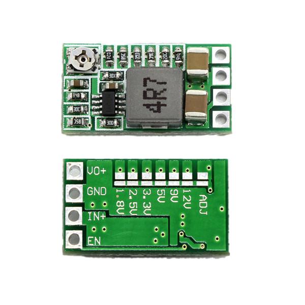
The red square in the bottom left is a MP2315 DC/DC regulator module:
