Author Topic: More voltage references - die pictures  (Read 55390 times)

0 Members and 2 Guests are viewing this topic.

Offline NoopyTopic starter

  • Super Contributor
  • ***
  • Posts: 1912
  • Country: de
    • Richis-Lab
Re: More voltage references - die pictures
« Reply #50 on: February 24, 2021, 12:06:43 pm »
 :-+

You have Mail!

Offline NoopyTopic starter

  • Super Contributor
  • ***
  • Posts: 1912
  • Country: de
    • Richis-Lab
Re: More voltage references - die pictures
« Reply #51 on: February 27, 2021, 12:25:58 pm »
...SZY22...

Of course I had to take a closer look into the SZY-references!  :-/O


I found a diagram showing the range of variation of the tempco of a zener back in the days. There is more than a factor of two! That explains why one diode could have been enough to compensate the positive tempco of the zener.


Now some more SZY22.  ;D


Now that we know how the diodes are packaged we don´t need to burn the epoxy but can cut and break the package.
There is some silicone potting protecting the diodes.


Here we have the three diodes described in the datasheet.  :-+


Breaking the glass body we can remove the diode itself. Here we see the residue of the die on the surface of the round contact electrodes.


The diode looks a lot more modern than the diodes in the 2-diode-SZY22. It looks like that is already a diffusion diode while the diodes in the 2-diode-SZY were built by alloying a metal into a silicon die.


SZY23, the SZY bin with the lowest tempco (10ppm/°C). This one was built by Röhrenwerk Mühlhausen.


No news...


...but more pictures of the diodes.  8)


Here the die is still on one of the contact electrodes.


The dies were sawn to some extend and then broken out of the wafer. (... ...grammer? ...well I´m no native speaker  ;D)


SZY22 (2-diodes): https://www.richis-lab.de/REF15.htm
SZY22 (3-diodes): https://www.richis-lab.de/REF17.htm
SZY23: https://www.richis-lab.de/REF18.htm

 :-+
 
The following users thanked this post: TiN, BU508A, RoGeorge, ch_scr, bill_c

Offline NoopyTopic starter

  • Super Contributor
  • ***
  • Posts: 1912
  • Country: de
    • Richis-Lab
Re: More voltage references - die pictures
« Reply #52 on: March 05, 2021, 08:38:17 pm »


400°C later => surprise: There are only two diodes.  :o

I have to correct myself. I´m a little embarrassed. Actually there were three diodes in the first SZY22. While putting parts in the archive I found the third diode in the burnt epoxy residues.  ::)  Sorry...

Offline NoopyTopic starter

  • Super Contributor
  • ***
  • Posts: 1912
  • Country: de
    • Richis-Lab
Re: More voltage references - die pictures
« Reply #53 on: October 02, 2021, 05:10:42 am »
« Last Edit: October 02, 2021, 06:05:14 am by Noopy »
 
The following users thanked this post: doktor pyta, BU508A

Offline NoopyTopic starter

  • Super Contributor
  • ***
  • Posts: 1912
  • Country: de
    • Richis-Lab
Re: More voltage references - die pictures
« Reply #54 on: January 19, 2022, 07:46:37 am »
For your information if you are just reading here:

I will decap the new ADR1399 but before doing this I had to update the LM399 and the MAC199. I have put these two updates here:
https://www.eevblog.com/forum/metrology/lm399adr1399/msg3950488/#msg3950488

I will put the ADR1399 in that topic too. In my view these references are VIPs as the ADR1000. The "more normal" voltage references will be posted here.  ;D
 
The following users thanked this post: MegaVolt

Offline TiN

  • Super Contributor
  • ***
  • Posts: 4543
  • Country: ua
    • xDevs.com
Re: More voltage references - die pictures
« Reply #55 on: January 20, 2022, 02:43:21 am »
Thank you for the awesome work and sacrifices  :D
YouTube | Metrology IRC Chat room | Let's share T&M documentation? Upload! No upload limits for firmwares, photos, files.
 

Offline NoopyTopic starter

  • Super Contributor
  • ***
  • Posts: 1912
  • Country: de
    • Richis-Lab
Re: More voltage references - die pictures
« Reply #56 on: January 20, 2022, 04:13:12 am »
May the god of electronics forgive me.  ;D

I´m exited every time I open up a new package. ADR1399 is really interesting too. Very similar to the LM399 but it is clearly a redesign, not just a copy.

Offline ramon

  • Regular Contributor
  • *
  • Posts: 143
  • Country: tw
Re: More voltage references - die pictures
« Reply #57 on: January 22, 2022, 04:36:47 pm »
Noopy, I have a request. No, it's not decapping some IC.

Please make a book. Those pictures are already amazing but your explanations and the replies from other members (hi magic!) are even better. No hurries. Not for this year or this decade, but please make it. 
 
The following users thanked this post: TiN, ch_scr, eplpwr

Offline NoopyTopic starter

  • Super Contributor
  • ***
  • Posts: 1912
  • Country: de
    • Richis-Lab
Re: More voltage references - die pictures
« Reply #58 on: January 22, 2022, 06:18:14 pm »
That's a nice idea. It definitely would have to be a picture book. :)
As soon as I find some free time I will think about it.  :-/O
 
The following users thanked this post: TiN, ramon

Offline NoopyTopic starter

  • Super Contributor
  • ***
  • Posts: 1912
  • Country: de
    • Richis-Lab
Re: More voltage references - die pictures
« Reply #59 on: June 11, 2022, 04:01:28 am »


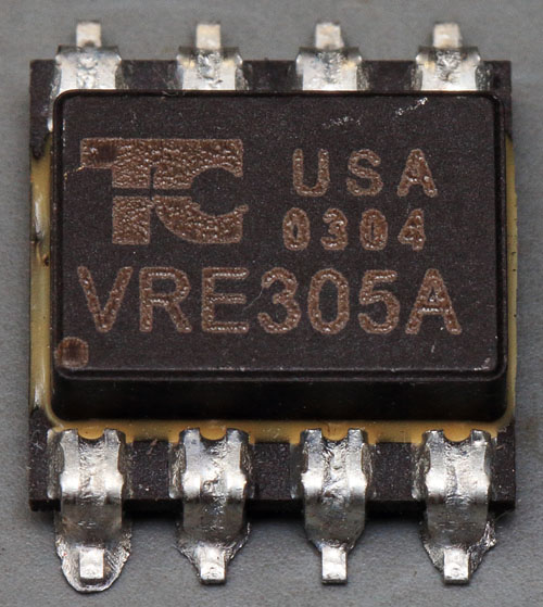
The VRE305A is a voltage reference developed by Thaler Corporation, now sold by Apex. Several variants exist with different output voltages from 2.5V to 10V, different packages and slightly different specifications.

The VRE305A delivers 5V with an initial tolerance of +/-0.5mV max and a temperature drift of 0.6ppm/K max. The long-term drift is 6ppm/1000h typ. The supply voltage must be at least 13.5V.
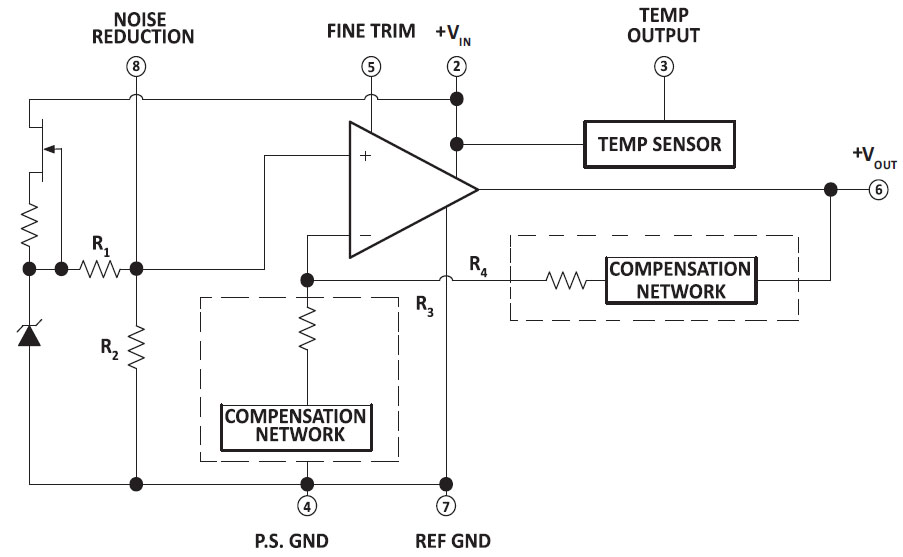


The datasheet contains a schematic that explains the operation of the VRE305A. The basis of the reference voltage is a 6.3V z-diode whose operating current is supplied by a JFET current source. A capacitor can be connected externally at pin 8 to reduce noise.

An opamp sets the desired output voltage with its gain factor. Resistors R3/R4, which define the gain factor, each contain a compensation network. According to the datasheet, this is a mixture of resistors and thermistors set to minimize the temperature drift of the reference voltage. The thermistors each make up just 2% of the total resistance so that they have as little effect as possible on the long-term drift.

Apparently one wanted to avoid setting the output voltage of the different variants by the resistor ratio R3/R4 and therefore integrated the voltage divider R1/R2 between the z-diode and the opamp. Pin 5 allows to adjust the output voltage a little. Other than shown in the schematic, this input influences the inverting input of the opamp. The VRE305A offers an additional ground pin, which allows to tap the reference voltage unloaded.

As will be shown in a moment, the temperature sensor is a simple diode whose operating current is set by a resistor.
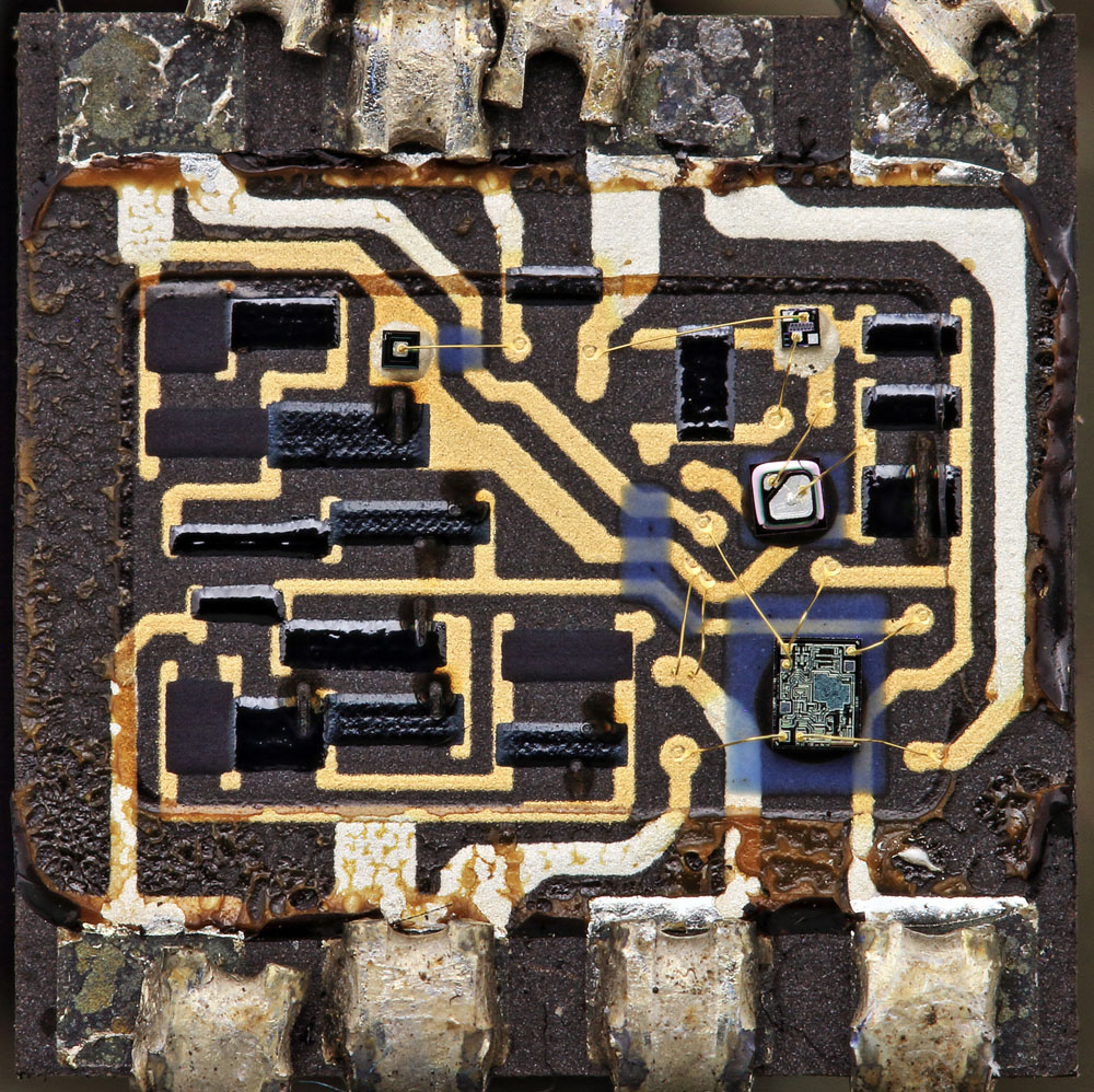
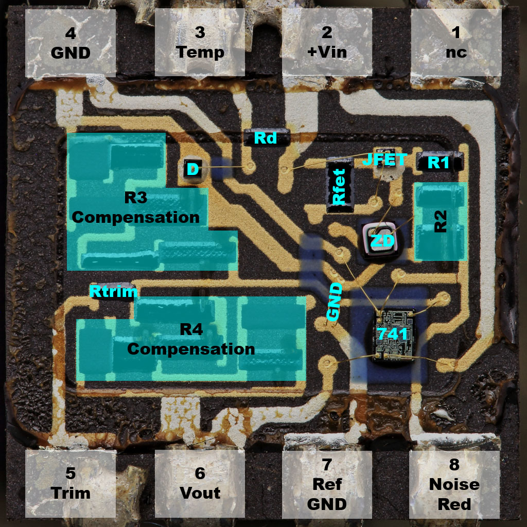


Under the cover there is a hybrid circuit. A large part of the area is taken up by the resistors R3/R4 with their compensation networks. The trim input influences the node between the resistors R3/R4 via the resistor Rtrim. The inverting input of the opamp is connected to this node too. The opamp is a National Semiconductor LM741. It has its own GND feed line.

The reference voltage source is located in the upper right corner of the board. The construction is the same as shown in the datasheet. The resistor R2 is divided into two areas of different size. Apparently these resistors are used to represent the different output voltages with little effort.

Pin 7, which is the GND for the reference voltage, is connected with two bonding wires to the z-diode so that this path is loaded as little as possible by the bias current of the diode.

At the top edge of the board is the diode, which can be used for temperature measurement. The resistor Rd provides the bias current.
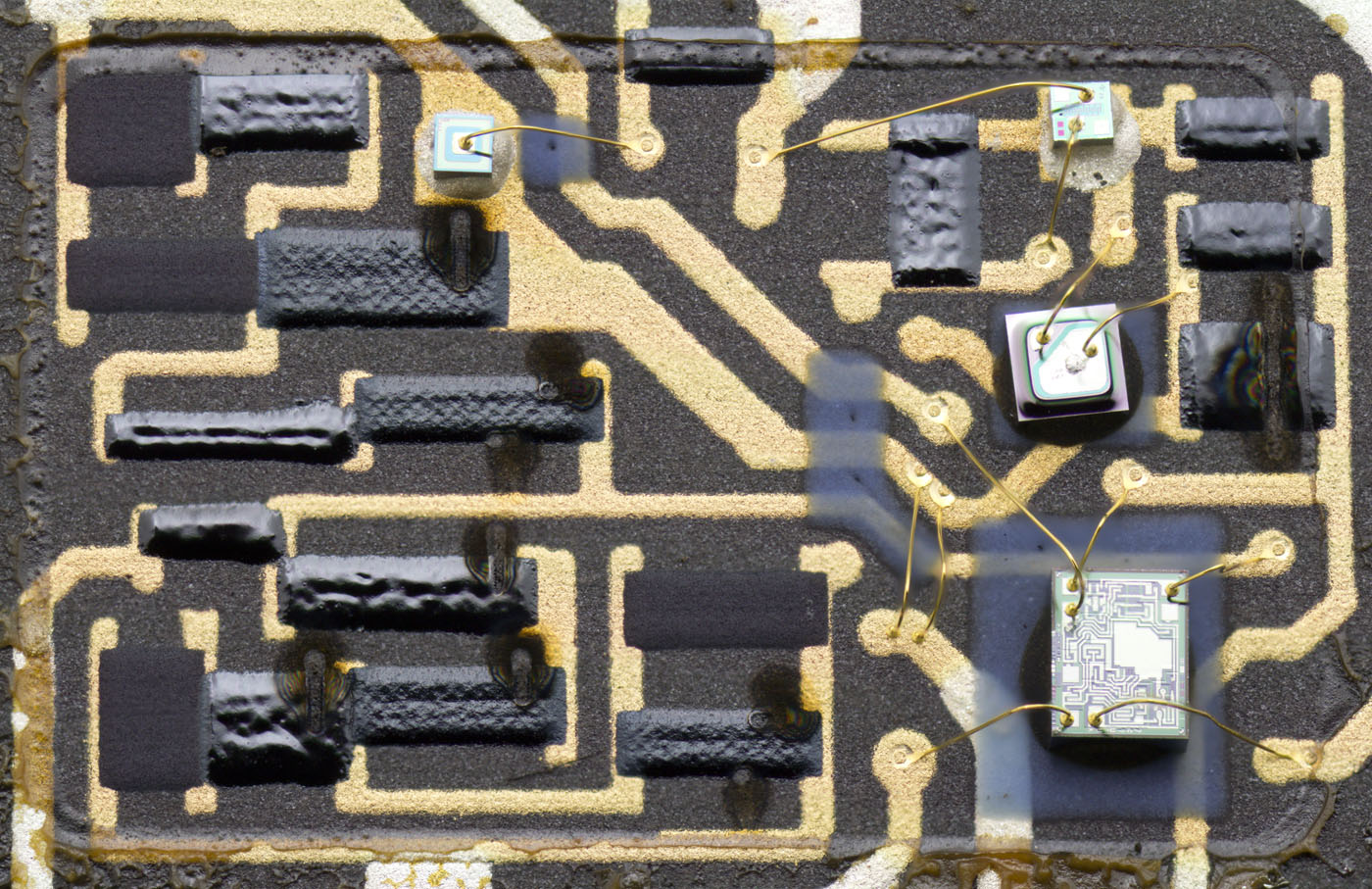


A lot of the resistors were laser tuned.
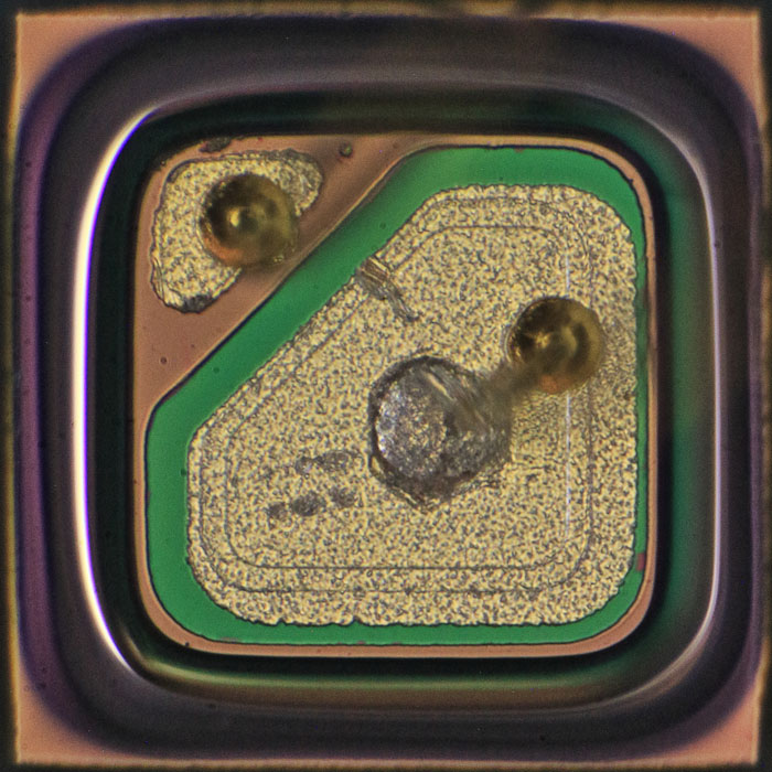


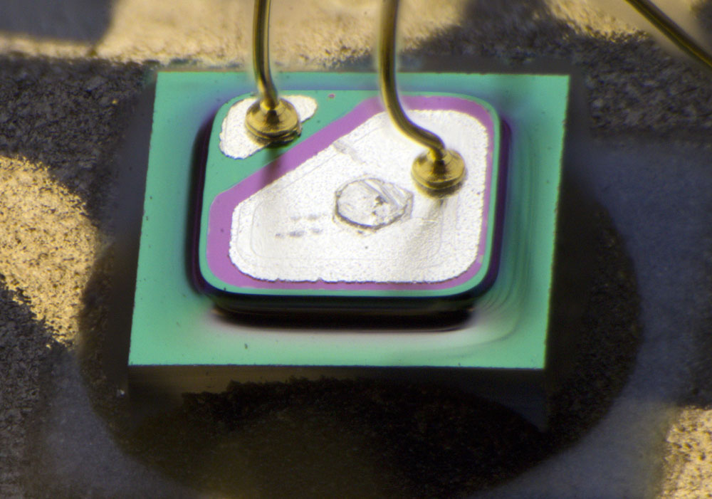
The edge length of the z-diode is 0.69mm. The design with the distinctive MESA structure is also found in the Burr-Brown DAC80 (https://www.richis-lab.de/DAC02.htm#ZD).
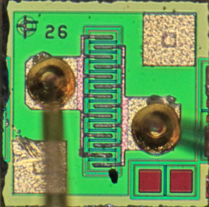


The edge length of the JFET is 0,37mm. The symbol in the upper left corner and the numbers 26 could be a hint to the manufacturer and the transistor type. Can anyone identify this part?

The bondwires feed the source and drain potential. The gate potential reaches the transistor through the substrate. The two bondpads in the corners of the dies would be alternative contact points for the gate potential. The blue elements between the source and drain areas represent the top gate electrode of the JFET. The green area is below the structures and acts as the lower gate electrode.

The test structure in the lower right corner appears to represent a large JFET.


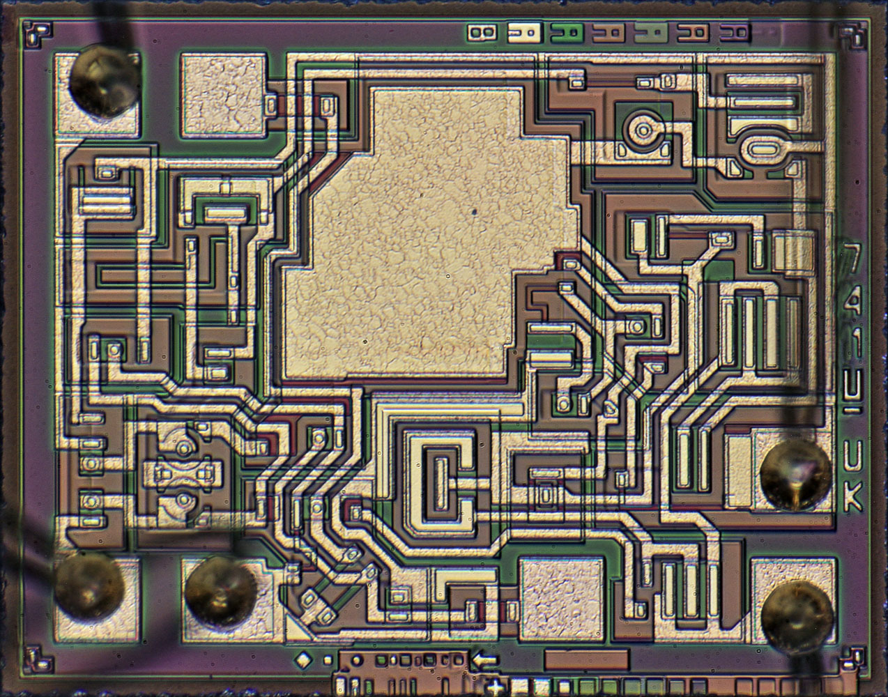
The opamp is a National Semiconductor LM741 (https://www.richis-lab.de/Opamp23.htm). On the right edge of the die there are the numbers 741. As described at the LM741 page the letter U after the numbers 741 is the revision of the design.


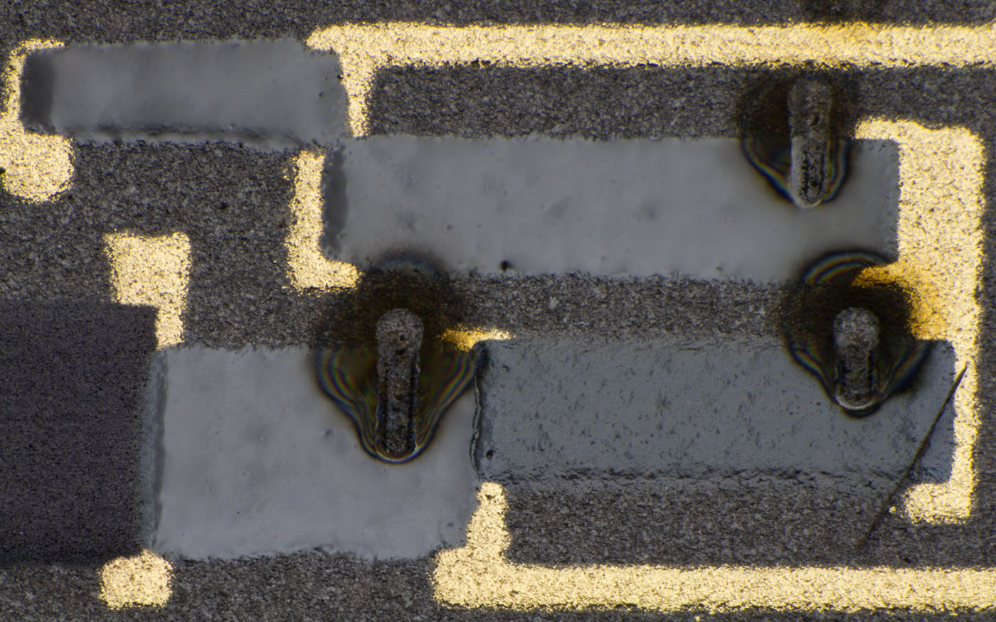
Three different resistor types appear to have been used in the compensation networks. In the bottom row, a resistor mass with a fine granular structure can be seen on the far left. This type of resistor has not been tuned. In the middle is a resistor with a smooth surface and on the right is a material with a more irregular surface. It can be clearly seen that the process of tuning has not only removed resistor mass but also heated a relatively large area of the environment.


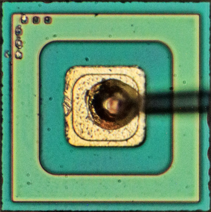
The edge length of the diode used for temperature measurement is 0,36mm. In the upper left corner there are small structures which probably allow to monitor the alignment of the masks and the quality of the manufacturing process.

The inner, darker area must be p-doped. The square that appears in the bond pad is the cutout through which the metal layer contacts the p-doped area. The light green frame must be n-doped and connected to the substrate. The substrate represents the cathode contact of the diode.


https://www.richis-lab.de/REF21.htm

 :-/O
 
The following users thanked this post: SeanB, chickenHeadKnob, Andreas, Vgkid, doktor pyta, BU508A, RoGeorge, iMo, Grandchuck, arcnet

Online Andreas

  • Super Contributor
  • ***
  • Posts: 3309
  • Country: de
Re: More voltage references - die pictures
« Reply #60 on: June 11, 2022, 05:11:00 am »
The edge length of the JFET is 0,37mm. The symbol in the upper left corner and the numbers 26 could be a hint to the manufacturer and the transistor type. Can anyone identify this part?
Hello,

Best guess: one of the two process geometries (N0026S/N0026L) of Interfet:

https://www.interfet.com/geometry-types/

so something like a J304/J305/J210/J211


with best regards

Andreas
« Last Edit: June 11, 2022, 05:14:29 am by Andreas »
 
The following users thanked this post: SeanB, Noopy

Offline NoopyTopic starter

  • Super Contributor
  • ***
  • Posts: 1912
  • Country: de
    • Richis-Lab
Re: More voltage references - die pictures
« Reply #61 on: June 11, 2022, 05:26:57 am »
Thanks Andreas!  :-+

Online iMo

  • Super Contributor
  • ***
  • Posts: 5284
  • Country: ag
Re: More voltage references - die pictures
« Reply #62 on: June 11, 2022, 11:00:11 am »
That VRE305 design looks as it could be easily tried at home :)
0.6ppm/K - hmm..
Readers discretion is advised..
 

Offline NoopyTopic starter

  • Super Contributor
  • ***
  • Posts: 1912
  • Country: de
    • Richis-Lab
Re: More voltage references - die pictures
« Reply #63 on: June 11, 2022, 11:11:12 am »
 :-+

And a good way to get rid of your old 741 opamps.  ;D
 
The following users thanked this post: iMo

Online iMo

  • Super Contributor
  • ***
  • Posts: 5284
  • Country: ag
Re: More voltage references - die pictures
« Reply #64 on: June 11, 2022, 11:27:13 am »
Hi Noopy, I have a couple of old 741 here, but this one is even older..
It waits to cooperate with the KZZ82 voltage reference..  :D
An inch by inch large box with 7 legs..


Readers discretion is advised..
 

Offline NoopyTopic starter

  • Super Contributor
  • ***
  • Posts: 1912
  • Country: de
    • Richis-Lab
Re: More voltage references - die pictures
« Reply #65 on: June 11, 2022, 11:58:12 am »
I have a similar one to decap but I'm not sure how to do it without killing the whole circuit. We will see...  :D

Offline RoGeorge

  • Super Contributor
  • ***
  • Posts: 6843
  • Country: ro
Re: More voltage references - die pictures
« Reply #66 on: June 11, 2022, 12:06:45 pm »


The edge length of the z-diode is 0.69mm. The design with the distinctive MESA structure is also found in the Burr-Brown DAC80 (https://www.richis-lab.de/DAC02.htm#ZD).
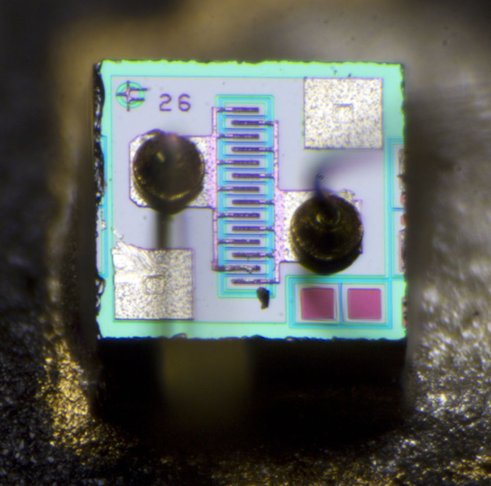
- Brain:  Hei, look!  The far away edge of the die is bigger than the near edge, the die is trapezoidal and distorted!  :scared:
- Chill down brain.  Let's put this transparent measuring ruler above the picture.  See?  They measure equal.
- Brain:  :o!?  Nope.  >:(

 ;D
 
The following users thanked this post: MiDi

Online Kleinstein

  • Super Contributor
  • ***
  • Posts: 14889
  • Country: de
Re: More voltage references - die pictures
« Reply #67 on: June 11, 2022, 01:10:06 pm »
The picture is very likely taken with quite some focus stacking and this can cause some distortions to the image.

It nearly looks like the right bond is already a 2nd try.

The hybird design looks a bid odd: the glue for the cover is in parts on top of resistors.
 

Offline mawyatt

  • Super Contributor
  • ***
  • Posts: 3934
  • Country: us
Re: More voltage references - die pictures
« Reply #68 on: June 11, 2022, 02:00:47 pm »


The edge length of the z-diode is 0.69mm. The design with the distinctive MESA structure is also found in the Burr-Brown DAC80 (https://www.richis-lab.de/DAC02.htm#ZD).

- Brain:  Hei, look!  The far away edge of the die is bigger than the near edge, the die is trapezoidal and distorted!  :scared:
- Chill down brain.  Let's put this transparent measuring ruler above the picture.  See?  They measure equal.
- Brain:  :o!?  Nope.  >:(

 ;D

This is a common result when the lens setup isn't telecentric, meaning the lens apparent magnification doesn't change with distance to subject. What happens is as the lens (or subject) is moved to allow stacking, the distance changes and this changes the apparent magnification and causes distortion in the final rendering.

This type of image distortion becomes a real headache when one is doing Stack & Stitch type work, where multiple images are collected in Z axis (optical), then subject (or lens) is moved in X and/or Y and another set of images collected in Z axis, and so on. Each position in X and Y is stacked in Z, then all results at X and Y are "Stitched" together in a chip panorama.

S&S became popular some time ago with insects, but our pioneering work on S&S chip images reveled the need for better control of the individual image distortions, since the chips can't be "fudged" together when stitching and seamlessly blended as easily as an insect or other non-orthogonal subject. This undesirable effect led to quest for better lens with lower distortion in the frame and better telecentric behavior....read more expensive  :(

Anyway with a near gigiapixel final rendering S&S image blown up the size of a wall, and not showing any appeared image fudging or blended, this required some very special custom lenses setups, fixturing and assemblies. When we pioneered chip imaging starting way back in ~2000, it took over a decade to figure out how to do this and everything was custom designed and built including stepper motor controllers, drivers, rails, lenses, camera interfaces and such, so lots of time and $ spent back then, but now this is straight forward.

Forgot to mention, this shows the how an image with significant depth relative to size is much more prone to lens artifacts (and other effects) than a planar image with little depth.

We know how much work is involved in chip imaging and Noopy's work is amazing and plentiful, so hats off  :-+

Best,   
« Last Edit: June 11, 2022, 02:20:13 pm by mawyatt »
Curiosity killed the cat, also depleted my wallet!
~Wyatt Labs by Mike~
 
The following users thanked this post: RoGeorge, Noopy

Offline NoopyTopic starter

  • Super Contributor
  • ***
  • Posts: 1912
  • Country: de
    • Richis-Lab
Re: More voltage references - die pictures
« Reply #69 on: June 11, 2022, 08:06:57 pm »
The picture is very likely taken with quite some focus stacking and this can cause some distortions to the image.

51 pictures / 1,1GB.  :-+


It nearly looks like the right bond is already a 2nd try.

You talk about the circle in the metal plane, do you?
You can see the same circle on top of the zener in the DAC80 (https://www.richis-lab.de/DAC02.htm#ZD). I assume that´s caused by the layer stack / architecture of the diode.


The hybird design looks a bid odd: the glue for the cover is in parts on top of resistors.

You are right. Seems they had no worries about that.  :-//


...

...

mawyatt has explained it perfectly.  :-+
BUT most of the time I change the focal plane by changing the focus of the lens. So I do change the magnification. Nevertheless there is still some distortion.

Offline razvan784

  • Regular Contributor
  • *
  • Posts: 91
  • Country: ro
Re: More voltage references - die pictures
« Reply #70 on: June 12, 2022, 06:08:52 pm »
Many thanks Noopy for taking your time to document all these devices. Your contributions are highly appreciated - technically, historically as well as artistically.

Regarding the mesa Zeners that seem to be integrated in multiple products by different manufacturers - can anyone speculate on their origin? Were they ever packaged discretely and might they be still available somewhere? They might be interesting to experiment with. I only found this old Motorola patent: https://patents.google.com/patent/US4775643A/en
 
The following users thanked this post: Noopy, arcnet

Offline NoopyTopic starter

  • Super Contributor
  • ***
  • Posts: 1912
  • Country: de
    • Richis-Lab
Re: More voltage references - die pictures
« Reply #71 on: June 12, 2022, 09:41:47 pm »
Many thanks Noopy for taking your time to document all these devices. Your contributions are highly appreciated - technically, historically as well as artistically.

Thanks for your nice words!  :-+
I really enjoy taking these pictures. Nevertheless it is always good to hear that there are people interested in such kind of pictures.


Regarding the mesa Zeners that seem to be integrated in multiple products by different manufacturers - can anyone speculate on their origin? Were they ever packaged discretely and might they be still available somewhere? They might be interesting to experiment with. I only found this old Motorola patent: https://patents.google.com/patent/US4775643A/en

Up to now I have no clue who was behind these zeners.  :-//

Online iMo

  • Super Contributor
  • ***
  • Posts: 5284
  • Country: ag
Re: More voltage references - die pictures
« Reply #72 on: June 13, 2022, 07:04:24 pm »
From that above patent:
"..P+ region 13 is on the order of 3-4 microns and P+ alloy region 22 has a depth of 5-7 microns with the whole substrate 11 having a thickness of about 8 millimeters.."
The biggest zener ever :)
Readers discretion is advised..
 

Offline NoopyTopic starter

  • Super Contributor
  • ***
  • Posts: 1912
  • Country: de
    • Richis-Lab
Re: More voltage references - die pictures
« Reply #73 on: June 26, 2022, 11:02:14 am »


The 1N829A is a temperature compensated Z-diode that can be used as a voltage reference. The manufacturer of the present model is unclear. It was installed in a larger module in 1984 and consequently cannot be younger.

The 1N821 to 1N829 Z-diodes offer two different reference voltages (5.9V-6.5V or 6.2V-6.9V at 7.5mA) and different temperature coefficients. The 1N829A is the best grade in this respect with a temperature coefficient of just 0.0005%/K.


As described in the context of the SZY22 (https://www.richis-lab.de/REF15.htm) a temperature compensated Z-diode consists of a Z-diode and one or more "normal" diodes connected in series. Correctly designed the temperature coefficients of the two diodes compensate each other almost completely.


The red varnish can be scraped off and the typical structure of a diode in a glass housing is revealed.


The largest part of the housing is occupied by the cylinders that contact the die. The die is round about 0,2mm thick.


If you break the glass housing you can expose the actual diode. The edge length of the die is 0,58mm.


A relatively thick metal layer makes it possible to contact the diode directly via the "large" cylinders.

A kind of frame can be seen at the edge of the dies. It seems like the process had some problems in the upper right corner.


Viewed from the side a relatively large gap can be seen on the other side of the diode. In simple diodes such as the SZY23 (https://www.richis-lab.de/REF18.htm) the die lies flat on one side and the substrate directly represents a full-surface contact.


If you remove the die you can see that the bottom (right) has a thick metal surface as contact just like the top (left). A frame structure can be found on the underside too.

The die was damaged during extraction but the structure is still clearly visible.


The design of the 1N829A is hardly surprising. A temperature compensated z-diode basically consists of two antiserially connected diodes. This structure can be realized by introducing p-doping into a n-doped substrate on both sides. This results in an pnp structure in which one diode is operated in "normal mode" and one diode is operated as a Z-diode.

This also explains why two variants of the temperature compensated Zener diode are referred to as "double anode" in the datasheet (1N822 and 1N824). According to the datasheet these diodes meet their specifications in both polarities. Most likely the two diode structures are always built the same way. Depending on the characteristics just a certain polarity is allowed or not.


https://www.richis-lab.de/REF22.htm

 :-/O
« Last Edit: June 26, 2022, 02:05:19 pm by Noopy »
 
The following users thanked this post: SeanB, Andreas, doktor pyta, BU508A, RoGeorge, alm, MiDi, ch_scr, macaba

Offline RoGeorge

  • Super Contributor
  • ***
  • Posts: 6843
  • Country: ro
Re: More voltage references - die pictures
« Reply #74 on: June 26, 2022, 01:36:59 pm »
Why 'double anode', when the die has two cathodes and a single anode, shouldn't that be called a 'double cathode' diode?
 
The following users thanked this post: Noopy


Share me

Digg  Facebook  SlashDot  Delicious  Technorati  Twitter  Google  Yahoo
Smf