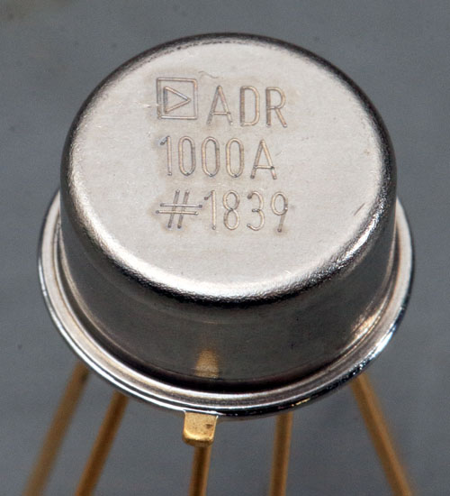
Of course I had to take some pictures of the ADR1000 too.

Special thanks to harerod (
https://www.harerod.de/) for donating the part.

In the ADR1000 pin 4 is connected to the case. In the LTZ1000 (
https://www.richis-lab.de/REF03.htm) the case wasn´t connected to pin 4 directly. There was just a connection through the substrate.
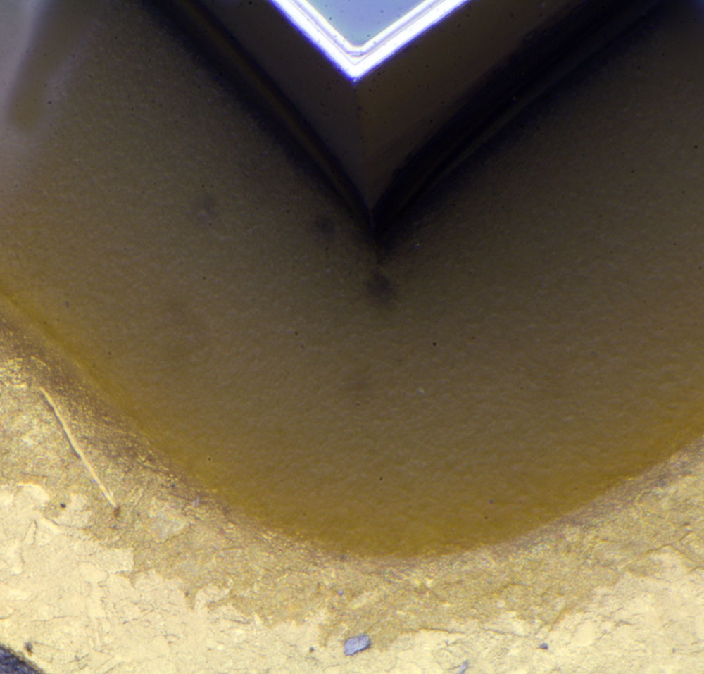
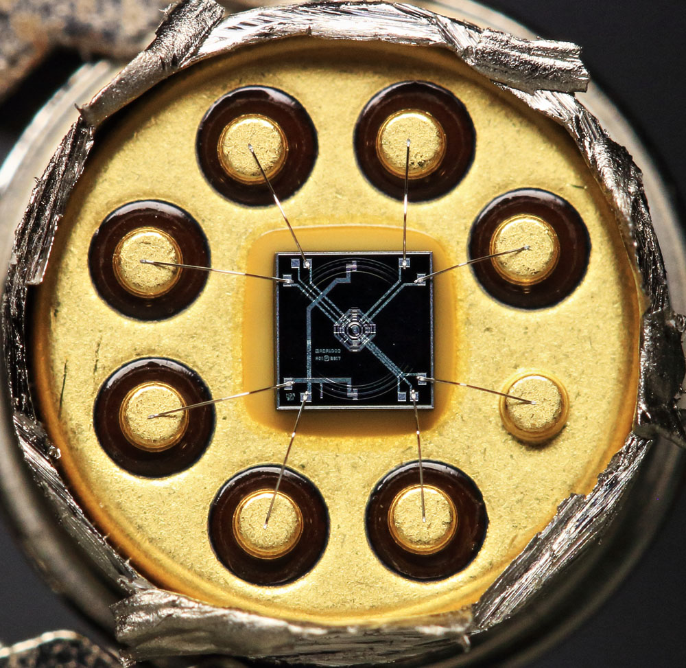
The die attache is done with some glue like material.
LTZ1000 was soldered which gave you a temperature resistance of 80K/W.
LTZ1000A was glued with some special fluffy polymer you can see in the LT1088 too (
https://www.richis-lab.de/LT1088.htm). The temperature resistance was risen to 400K/W.
For the ADR1000 216K/W had to be good enough.
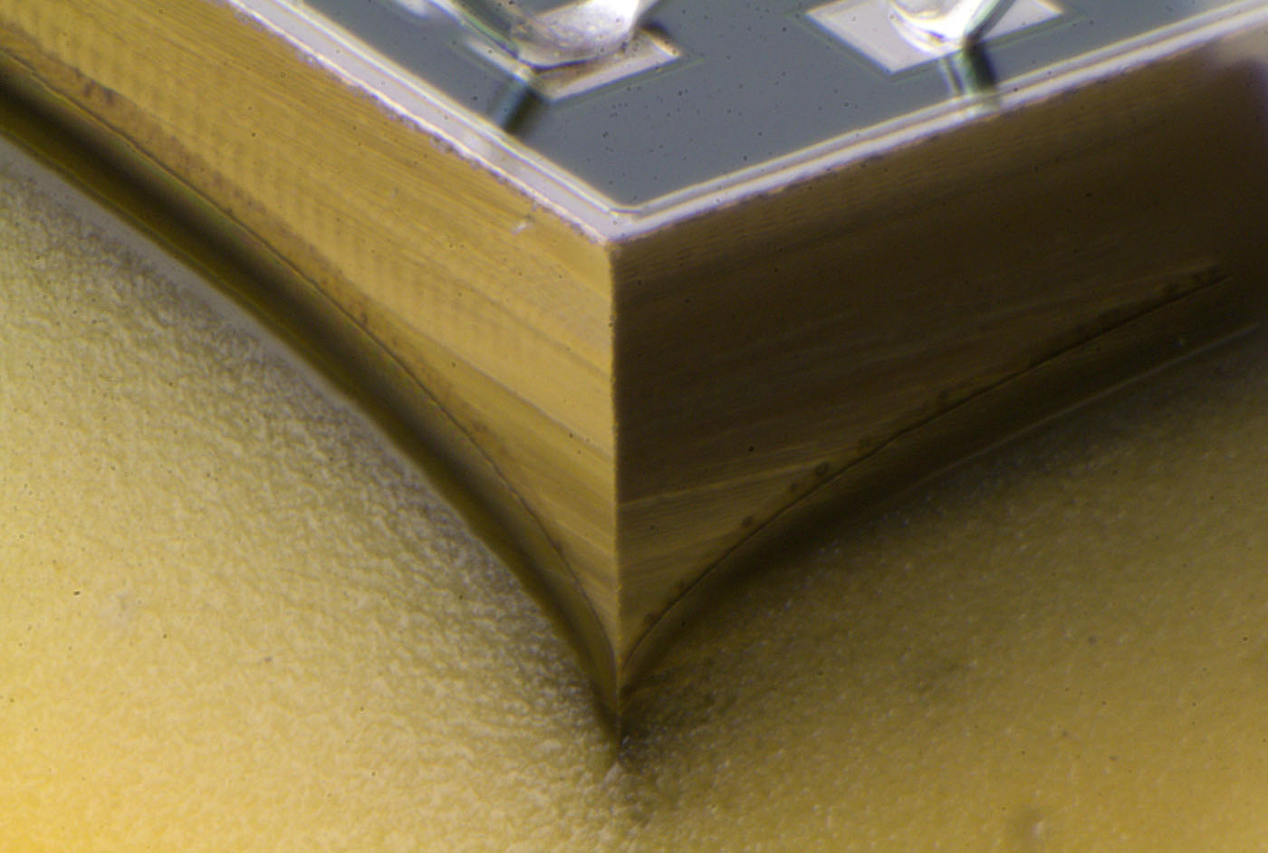
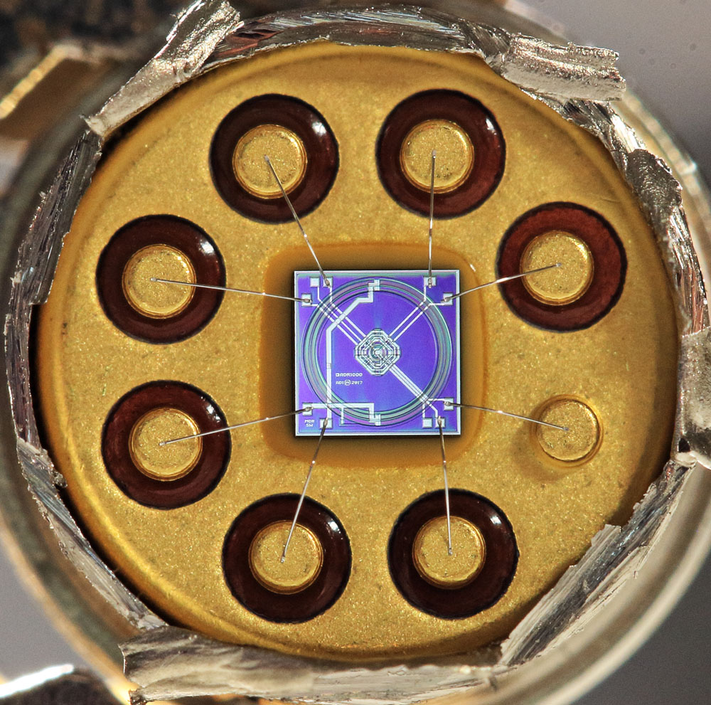
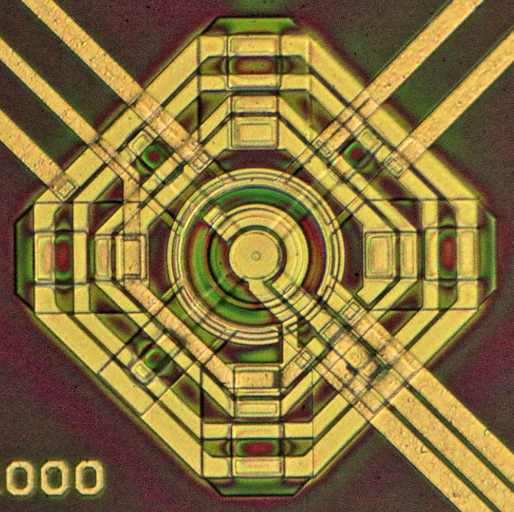
A very clean edge! Perhaps it´s normal. Perhaps they expended effort to get cleaner edges since impurities due to sawing of the wafer can worsen the stability?
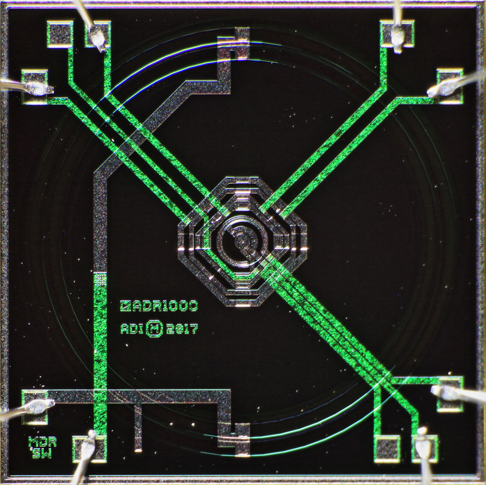
Analog applied two layers of metal.
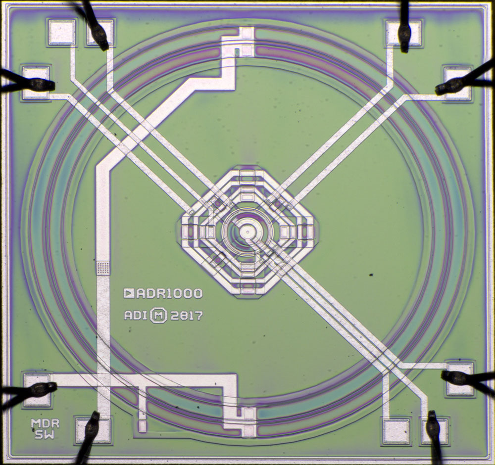
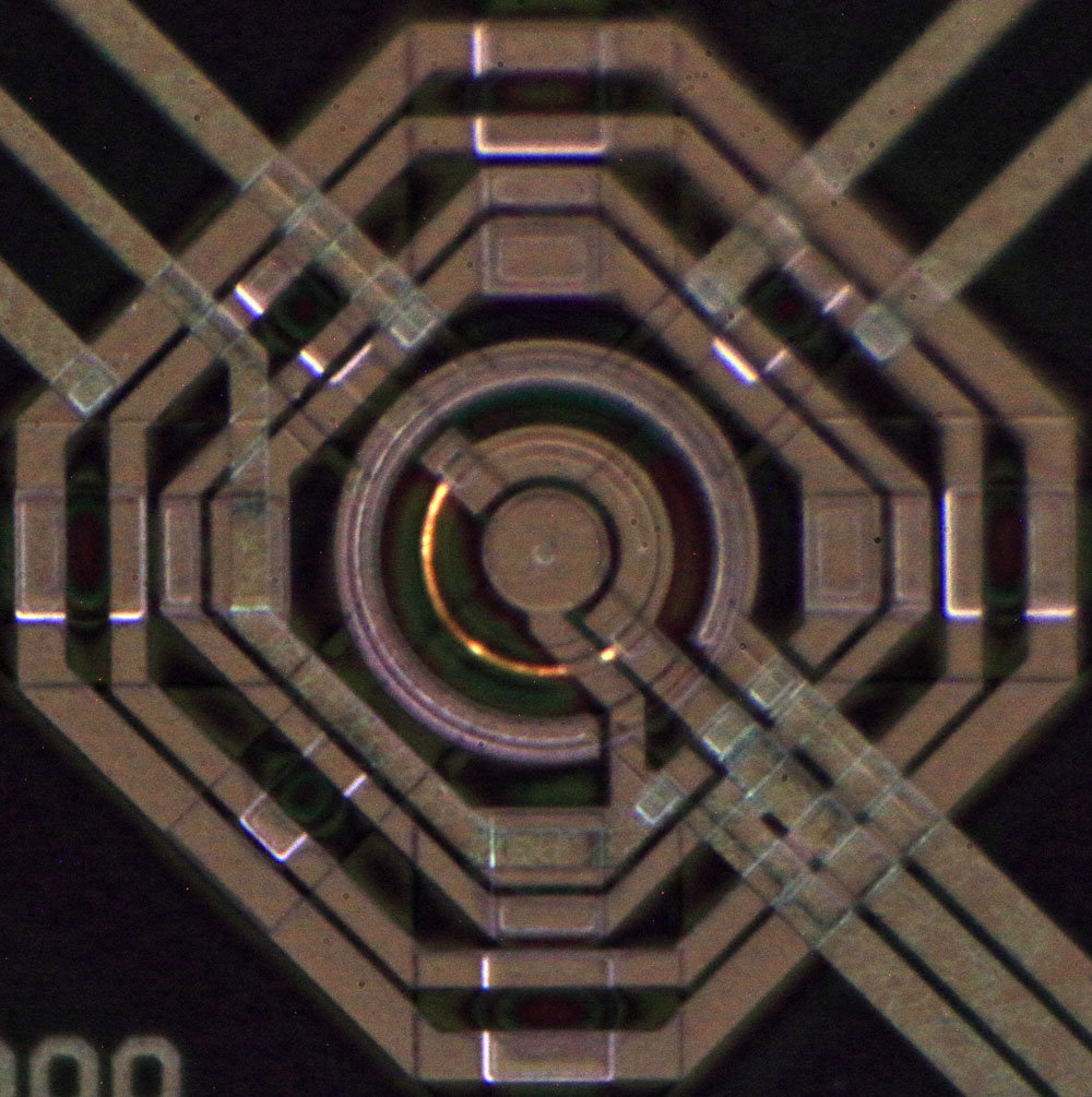
ADR1000 is quite similar to the LTZ1000 but the heater structure is much simpler, no more spare structures.
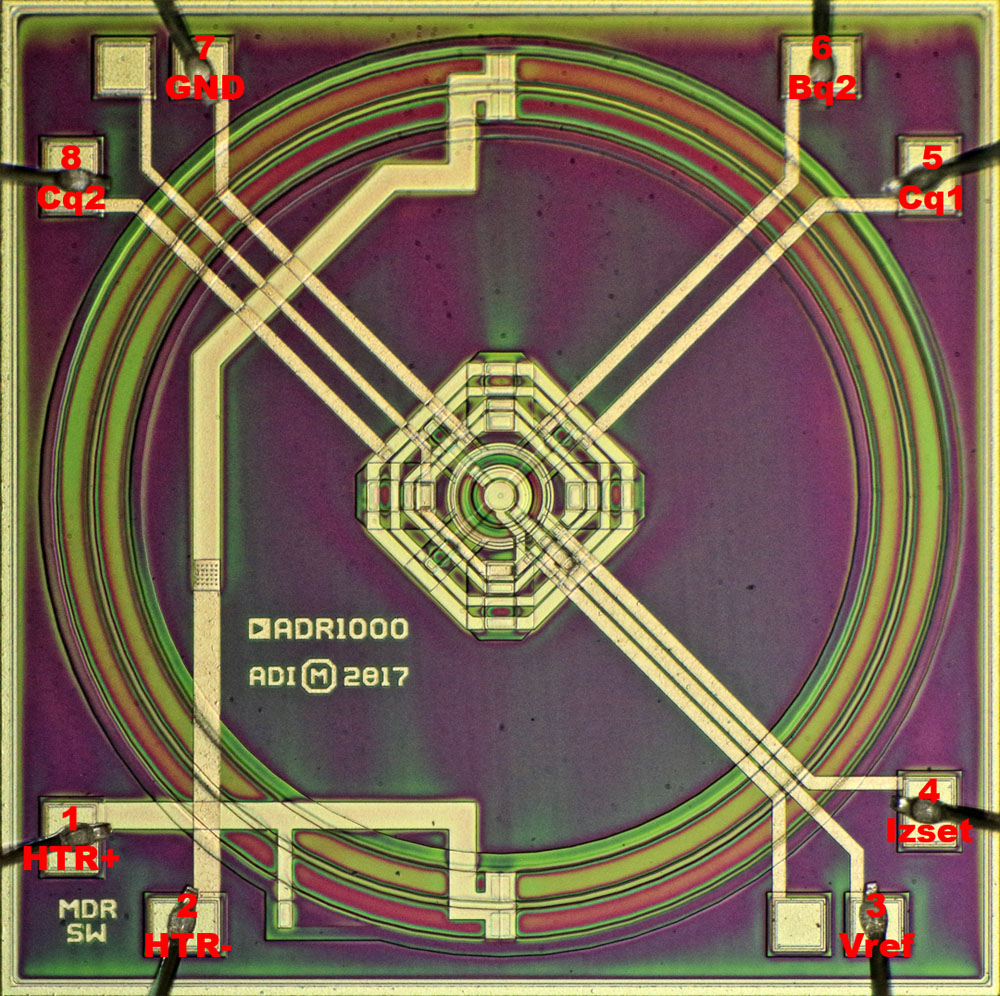
Let´s take a closer look at the circuit. There are two additional bondpads leading to the reference circuit.
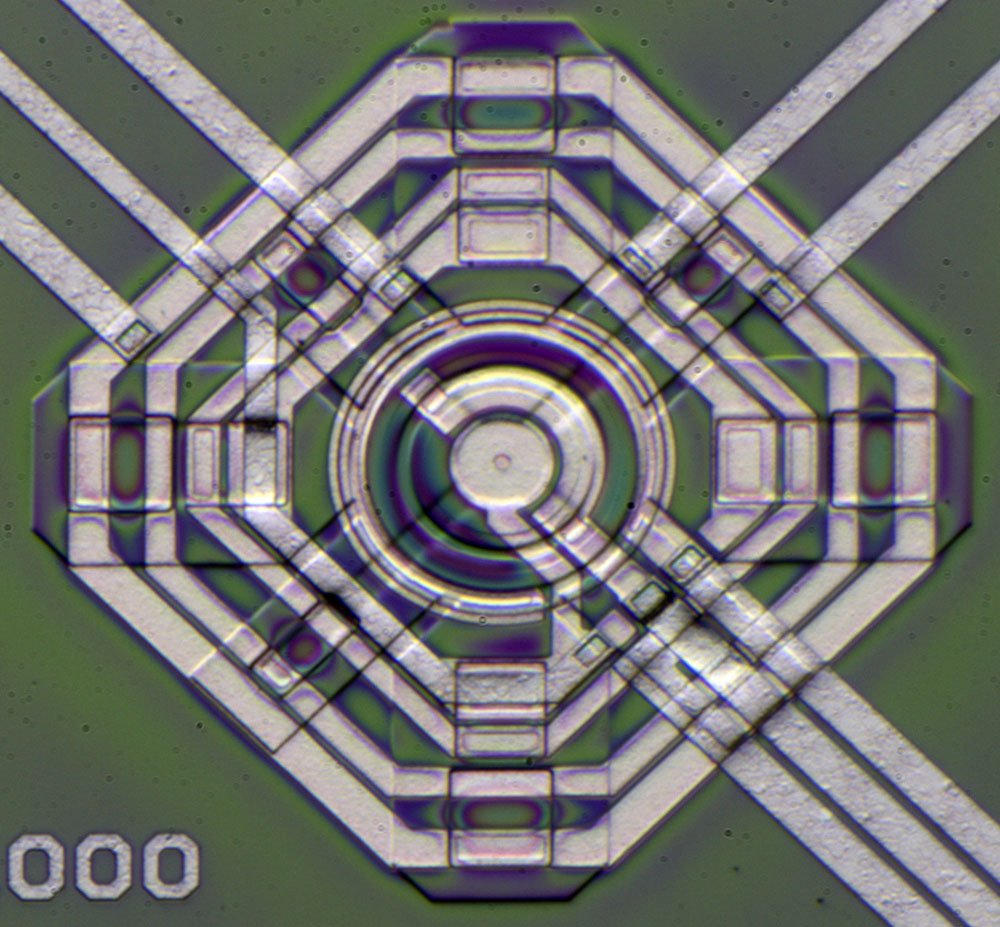
With the two metal layers the circuit is a little harder to read...
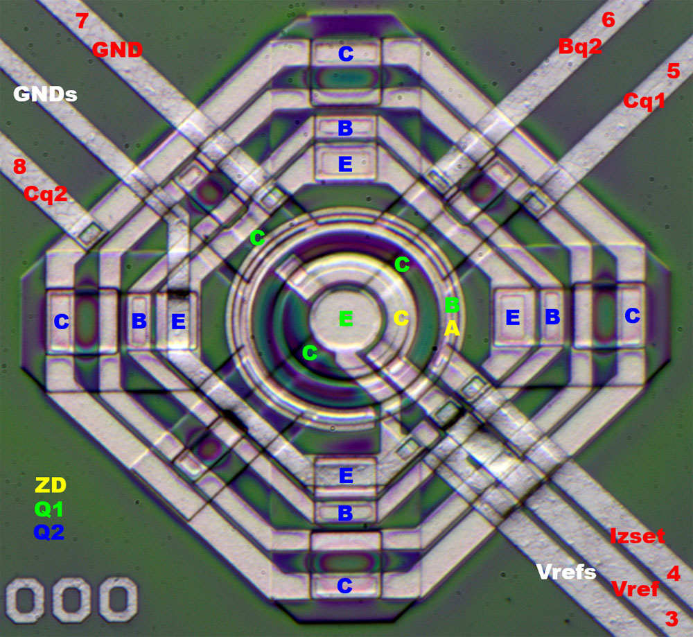
The active parts are the same as in the LTZ1000 but here we have the possibility of a 4-wire-connection! VREF and GND are connected a second time directly at the zener-transistor-combo so the bias current and the traces conducting the current don´t interfere with the reference voltage. The sense traces are connected to the two unused bondpads.
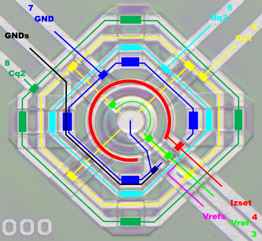
Trying to clarify the connections.
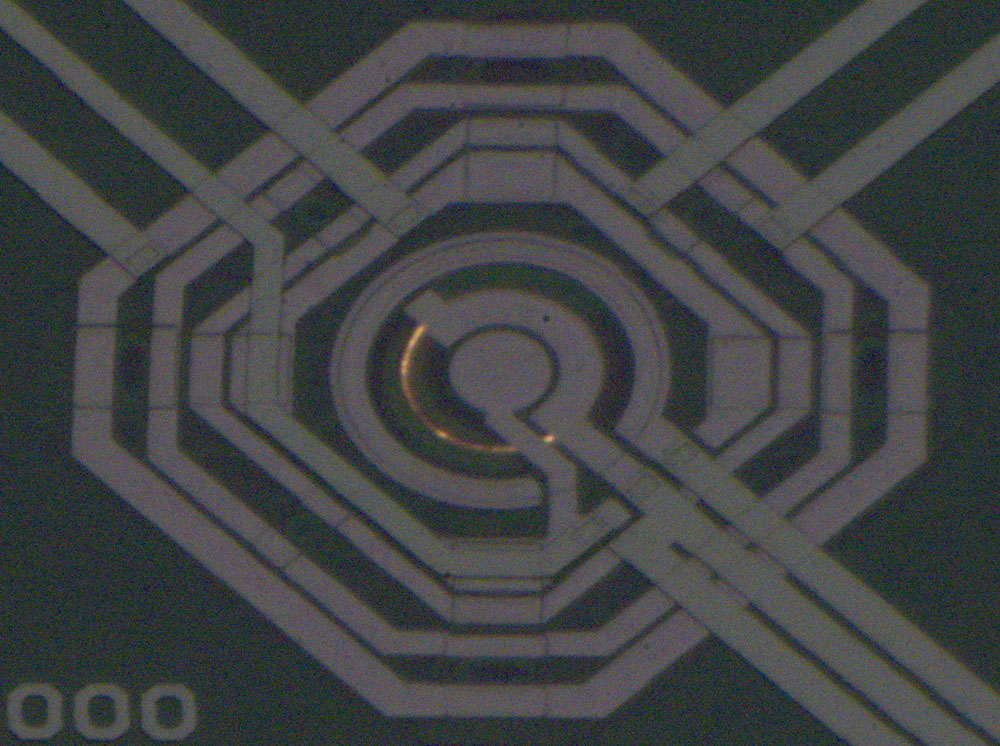
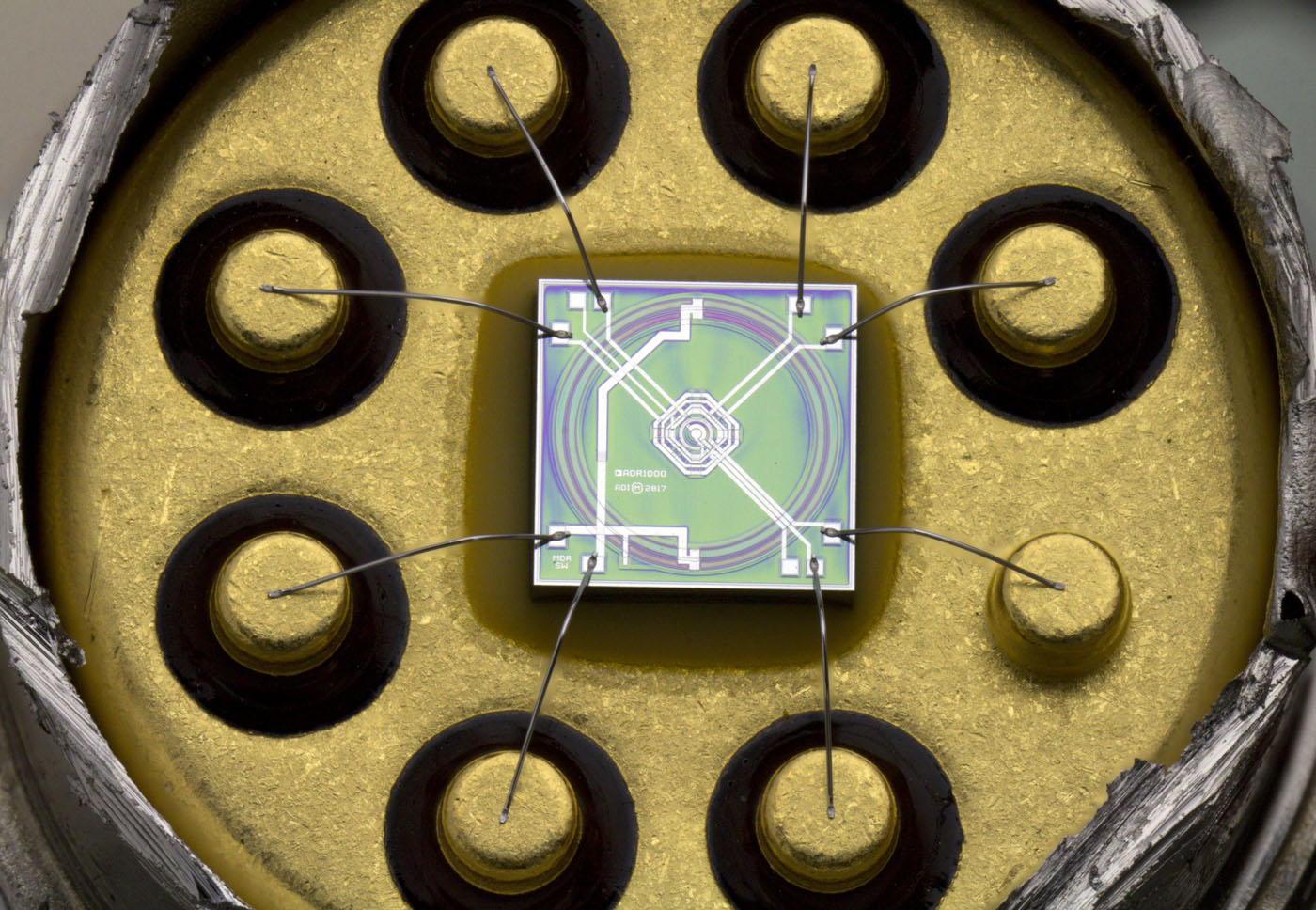
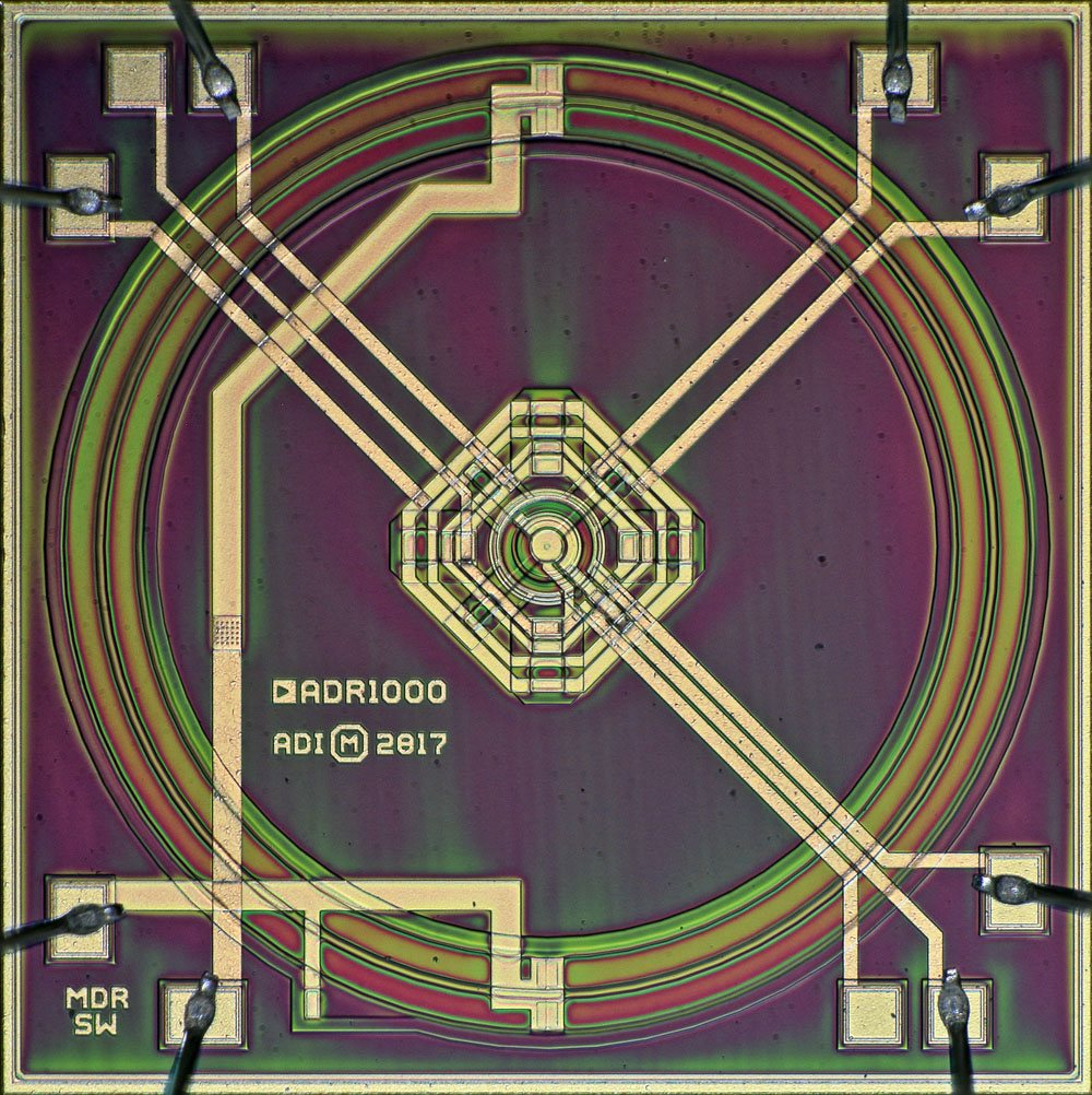
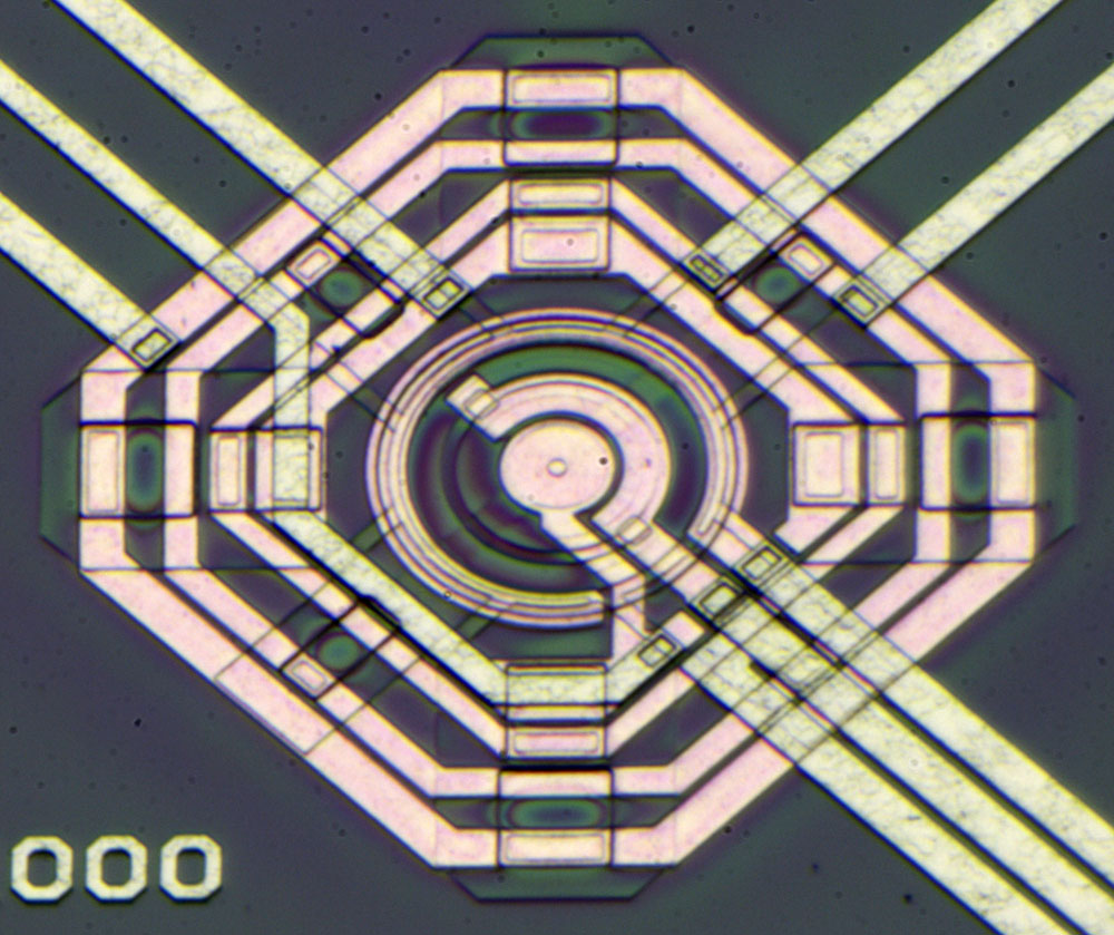
And of course I had to light it up (5mA).
It looks like the light is more uniform than in the LTZ1000. Perhaps here we see one reason for the lower noise figure? A more uniform structure in the buried zener?
https://www.richis-lab.de/REF19.htm 


