A long time ago I have taken some pictures of the LM399 and the MAC199 (
https://www.eevblog.com/forum/projects/lm399-die-analysis/msg2875790/#msg2875790) and tried to analyze the circuit. Now that I have a ADR1399 I first have to do an update on the LM399 and the MAC199. Putting the update in this topic here seems to be sensible.
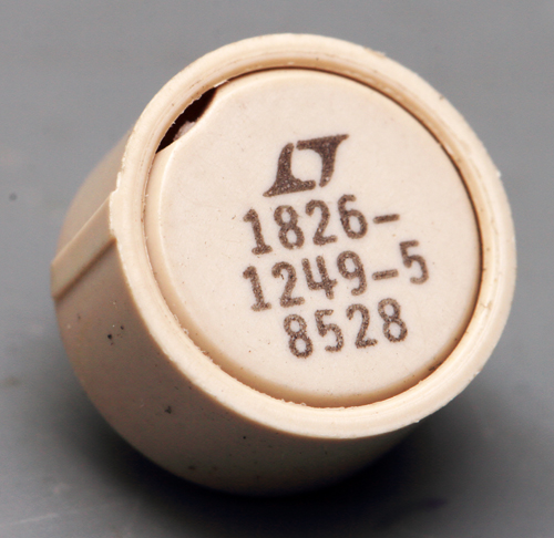
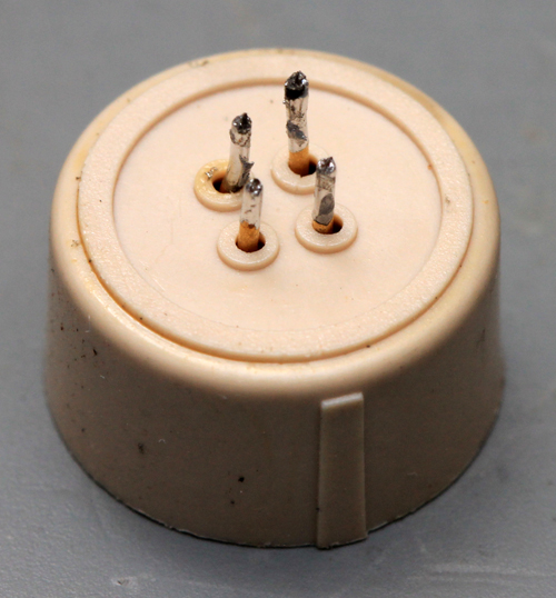
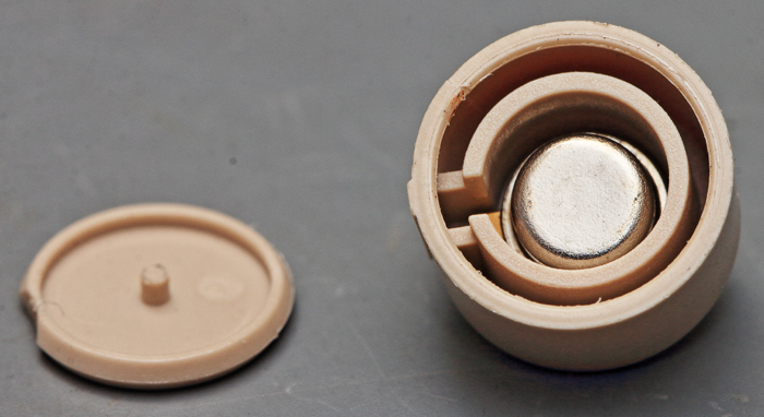
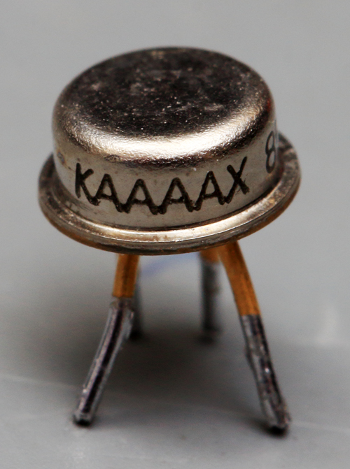
Well you know the package.
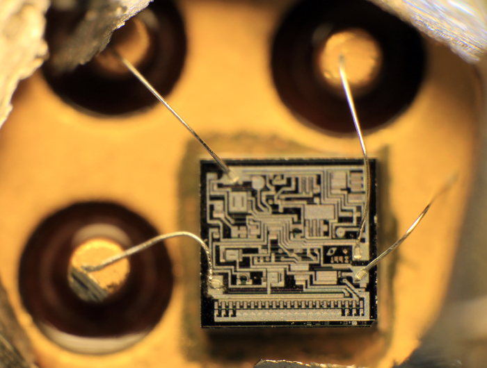
Quite a big die for the small TO-46 package. (Yes, that´s an old picture.

)
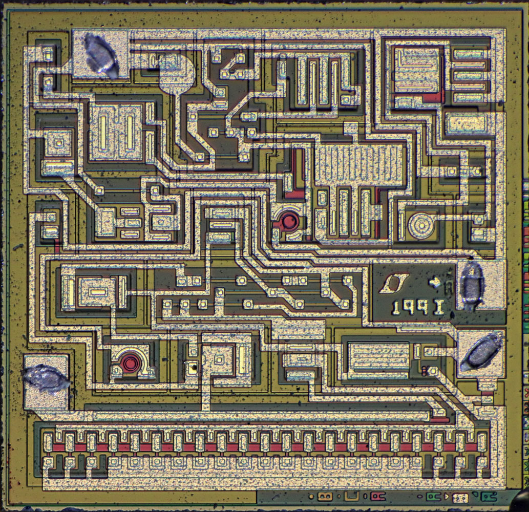
This picture is a little better than the old one. 199I stands for LM199, the variant with a higher temperature rating.
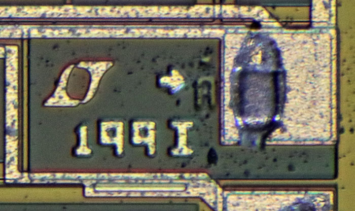

At the lower edge there are the revisions of six masks. One more revision marking is near the bondpad of pin 1. The arrow highlights bondpad 1.
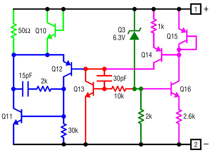
The LM399 is a shunt regulator. The power part (blue) is built with a sziklai pair. The RC prevents oscillations. The 50R (green) is the emitter resistor for the sziklai pair. It is protected by Q10. If there is to much current flowing through the resistor the transistor opens a bypass.
Q3 (dark green) is the reference, the buried zener. The current necessary for the zener is determined by the 2k resistor.
The red part drives the sziklai pair. If the voltage across the terminals of the LM399 increases, the voltage across the 2k resistor is increasing, increasing the current through Q13, increasing the current through the sziklai pair and finally reducing the voltage across the terminals of the LM399. The RC prevents oscillations.
The pink part is a feedback biasing Q13. A voltage higher than 6,9V at the LM399 terminals gives you more current flow through Q13 and more current through Q16 too. The current mirror Q14/Q15 feeds the current into the node Q12/Q13 working against Q13 sinking current to lower the voltage across the LM399. This is probably for biasing Q13 into an ideal operating point. But it´s interesting that the bias increases with increasing deviation of the voltage across the LM399.

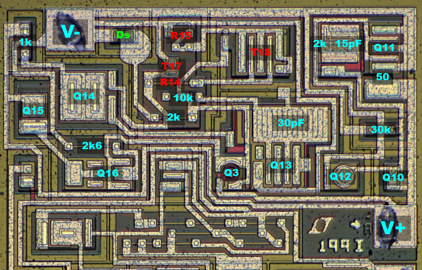
The shunt regulator is in the upper part of the die. In addition to the parts in the schematic you can find the diode between heater and regulator ground (green) and some more parts at the upper edge of the die (red).
The 10k at the base of Q13 can be tuned.
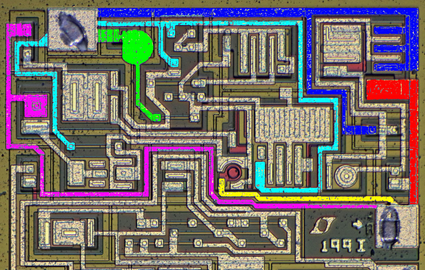
A nice starpoint supply.

The shunt regulator is connected to red/blue. The zener is supplied by yellow/green and the rest of the circuit is connected to pink/cyan.
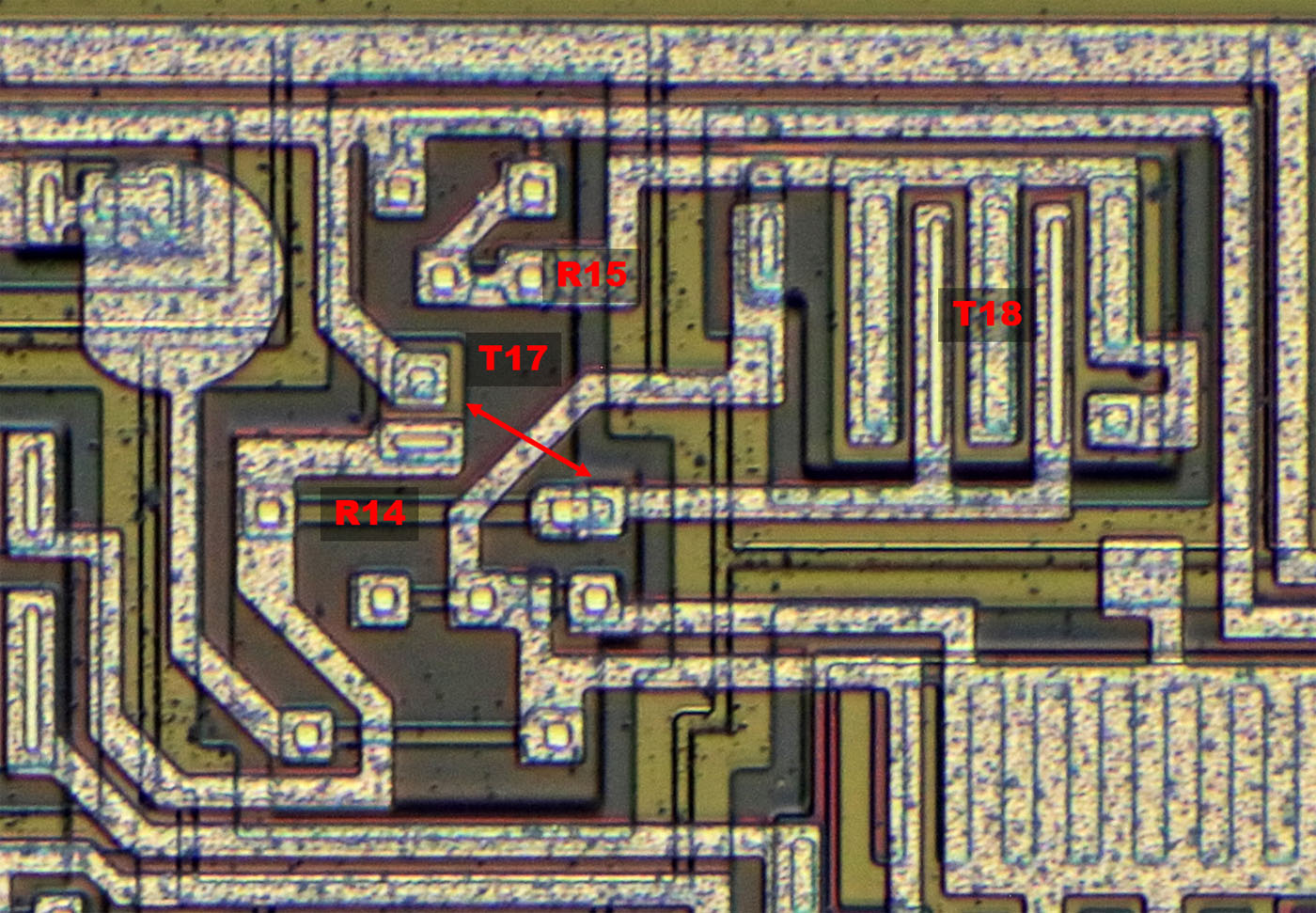
Here you can see the additional circuit. T17 is hard to recognize. The right contact of the resistor R14 connects to the n-doped well too and acts as a collector for T17.
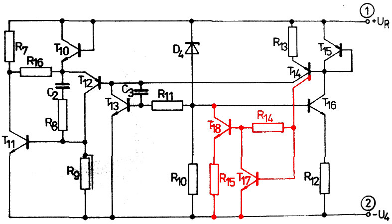
Tesla has copied the LM399 (MAC199). In the schematic of the MAC199 you can find the additional circuit (red). It looks like it is an additional current sink for the zener. T17 does some current limiting.
I have no idea why they integrated this circuit.

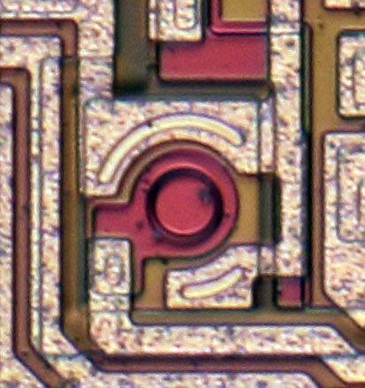
The buried zener diode…
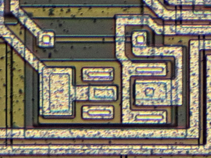
The transistor Q16 is interesting. It seems it has a big and a small collector contact, four base contacts (two of them connected) and one emitter contact. A lot of options…
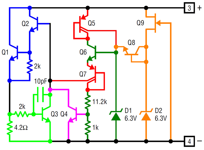
The Darlington pair Q1/Q2 (blue) is the heater. The green circuit is an overcurrent limiter.
The dark green circuit generates a reference current for the two current mirrors (red). Q7 biases the driver circuit. Q4 (pink) is the temperature sensor. With a higher temperature Vbe drops drawing more current of Q7 and reducing the current trough the Darlington stage.
Q5 supplies D1 with a constant current. The orange circuit supplies a voltage at start-up. Q8 isolates the start-up circuit as soon as the reference circuit is active.
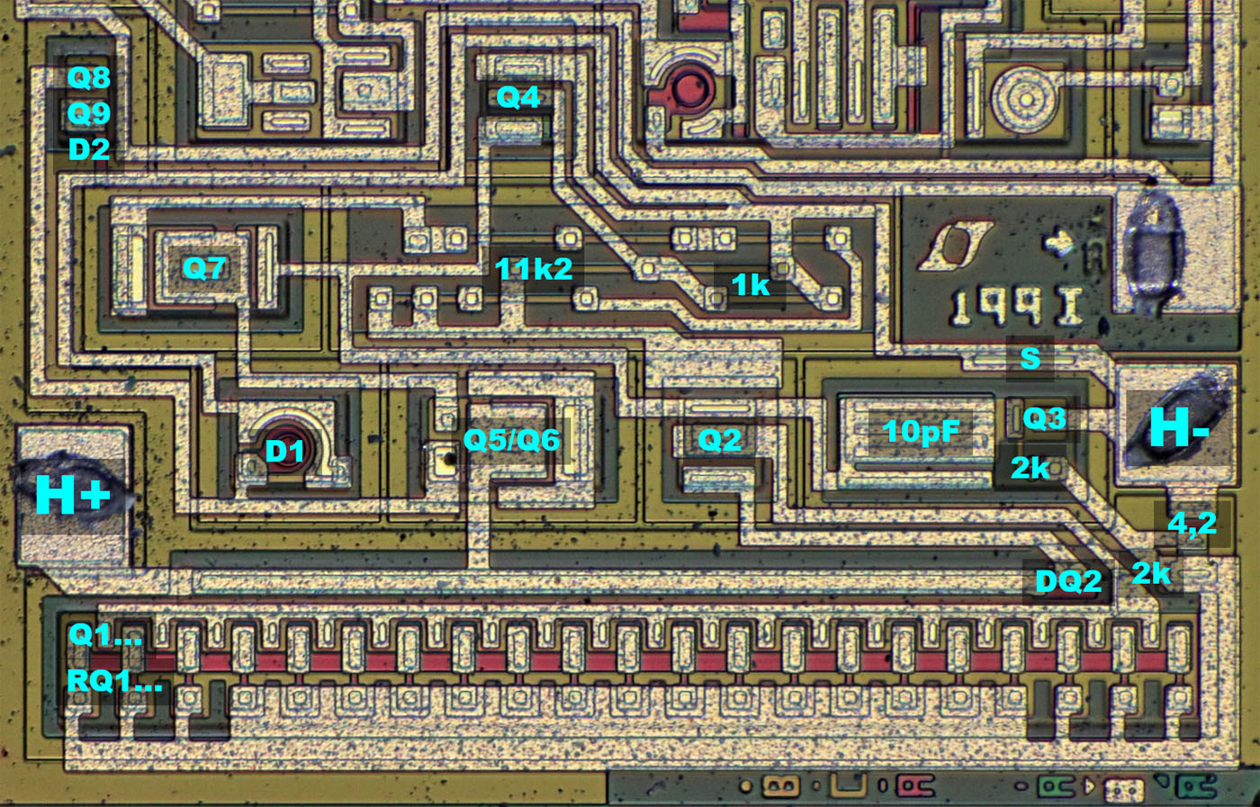
At the lower edge there is the big transistor Q1 which consists of 21 transistors. It has to dissipate up to 5,5W. The 4R2 resistor of the current limiting circuit can be adjusted.
In the heater circuit you can find the diode ZD2 above the transistor Q2. The MAC199 schematic shows this diode. It lowers the potential of the transistor Q2 so it´s easier to drive it.
The temperature sensor Q4 is near the reference zener. The voltage divider 11k2/1k allows a lot of different connections which moves the desired temperature.
The combination Q8/Q9/D2 is integrated quite efficient.

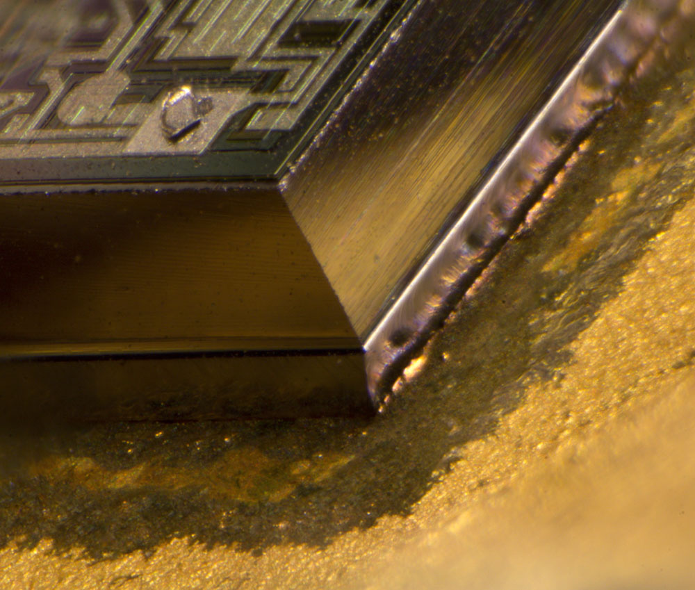
In the first place I guessed the die is placed on an additional layer that protects the reference circuit from mechanical stress. Today I assume the rough edge is due to breaking of the wafer after sawing the upper part.
https://www.richis-lab.de/REF02.htm 