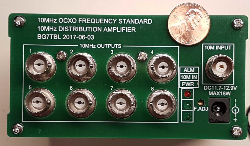
Recently, I purchased an inexpensive 10 MHz distribution amplifier on Ebay (fig. 1 - NB: the penny is there to give an indication of size. For those unfamiliar with US pennies, they are about 18 mm in diameter). I tested the unit and discovered it had a defect (channel 2 output a 430 mV sine wave, whereas all others output a 3.3V sine wave). During the process of investigating what was the problem in consultation with the seller, I opened it up and took some photos. Ultimately, the seller and I could not come to an agreement how much discount of the original price I should receive to fix the amplifier (which was advertised as brand new), so I shipped it back to him for a refund.
Figure 1

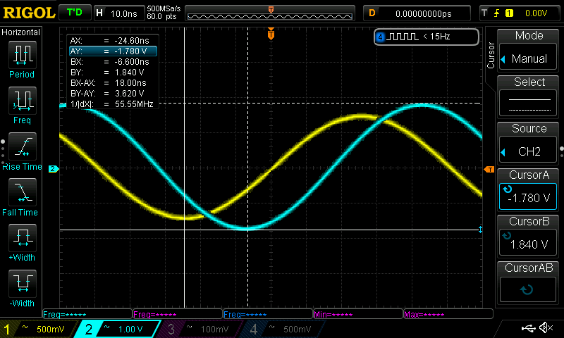
However, I thought readers of this forum might be interested in the characteristics of the unit and what it looks like inside the case. Fig. 2 shows the input to the amplifier (yellow trace) and the output signal on channel 1 (blue trace). Notice that the input is 1.5 V P-P and there is a phase shift between the input and output of 18 ns. Since the period of a 10 MHz signal is 100 ns, the phase shift is about 65 degrees. This shift is probably due to delays through signal preprocessing components, including an inverting buffer suitable for driving a 50 ohm load (see below).
Figure 2

Fig. 3 shows the same two signals with the measurement cursors bracketing the output signal, which is 3.62V P-P.
Figure 3

Fig. 4 shows the phase shift on channel 5, which is 17.6 ns. This represents 63 degrees of phase shift. Consequently, the phase shift varies by several degrees on each channel, even when those channels are roughly in phase.
Figure 4

Fig. 5 shows the phase shift on channel 3, which is 67.8 ns. This is 244 degrees of phase shift. It appears that channel 3 is 180 degrees out of phase with an additional 65 degrees due to delays through the inverting buffer.
Figure 5

During the negotiation between the seller and me, I obtained from him a partial schematic of the board. Since I do not have his permission to post that image, I have reproduced some of it using LTSpice. This is shown in figure 6 (ignore the component identifiers, since they do not correspond with the board identifiers, which are shown in the next figure).
Figure 6

Fig. 7 shows the bottom of the PC board. The input sine wave arrives on the left side, is filtered then converted from a sine wave to a square wave (according to
glarrson post) and then fed to a 74LVC2G04 buffer. The output of the buffer is filtered to obtain a sine wave and the result presented at the BNC connector of the associated channel.
Figure 7

The schematic is fairly unremarkable, the only somewhat interesting point being the use of the 74LVC2G04, which sources a high current signal sufficient to drive a 50 ohm load. There is nothing in the schematic that suggests why 4 channels are over 180 degrees out of phase with the other 4 channels. I attempted to trace the signal on the photo of the PC board bottom from input to output channels in order to identify the reason for the phase shift, but was unsuccessful.