Hi all,
This is my first topic, but I've been a lurker for some time, and been watching eevblog since 2008. I enjoy teardowns and understanding how things work quite a bit and I take a lot of pictures and whatnot. I was talking to a friend and they recommended that I start posting them here for others to enjoy so that's what I'm doing now. I have some devices that I wasn't able to find any teardowns of and some have very little info at all.
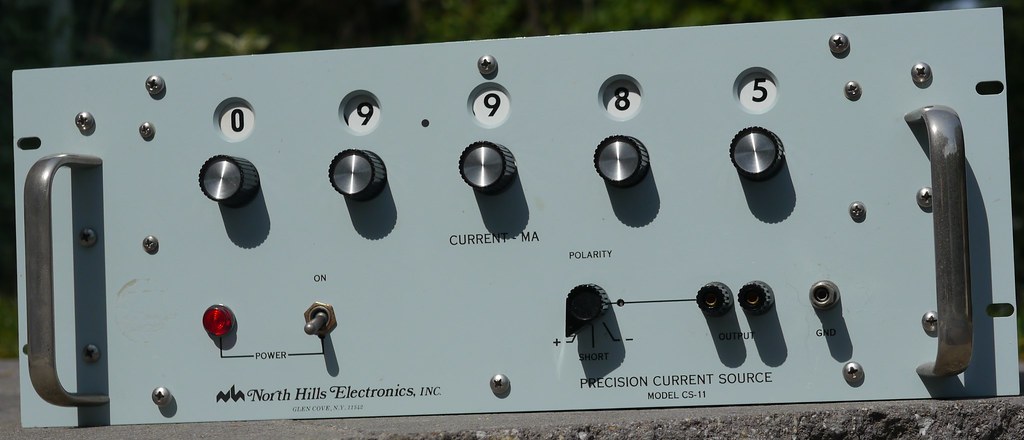
The first is a "north hills" CS-11 Precision current source. This is a huge and very old school unit. Unfortunately I wasn't able to find any manual for this online. I'm about 3/4 the way done writing the schematic and will post that here when it's ready. It has 5 decades and can go from 1 uA to 99.999 mA. Using it with my DMM, it seems to be pretty close to that, but I'm waiting to take some better measurements. This unit is from 1988 according to one of the voltage regulators, but the other IC's are from 1983-86 so I imagine it was in production for several years.
I'm still thinking up a good workflow for posting pictures, so I've got this as a 1024*440 pixel preview that you can click on for full resolution. All my photos are CC-BY so feel free to share with attribution.
Despite being quite large, this unit is very lightweight due to being mostly empty space inside.
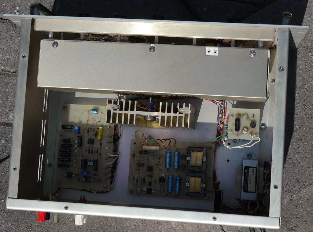
Inside you can see very old school construction. The unit is broken up into logical blocks and they are connected together with a really nice wire loom with cable ties. At the top of the frame is the shielded box with the big rotary switches and resistors in it.
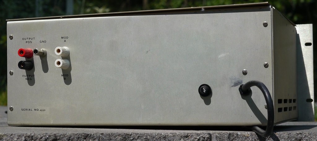
Even the rear is quite sparse with an additional output and a fuse. I don't know what the "mod" jacks do, but we'll have a better idea once I finish with my schematic.
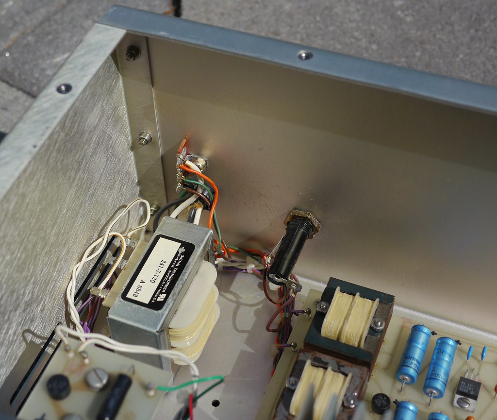
After the fuse and the switch, power comes in through this transformer which looks to be the newest thing in this unit.
Basic and very old school regulation: diode bridge, enormous capacitor. It still takes about 10 seconds to discharge the capacitor, even with that resistor there.
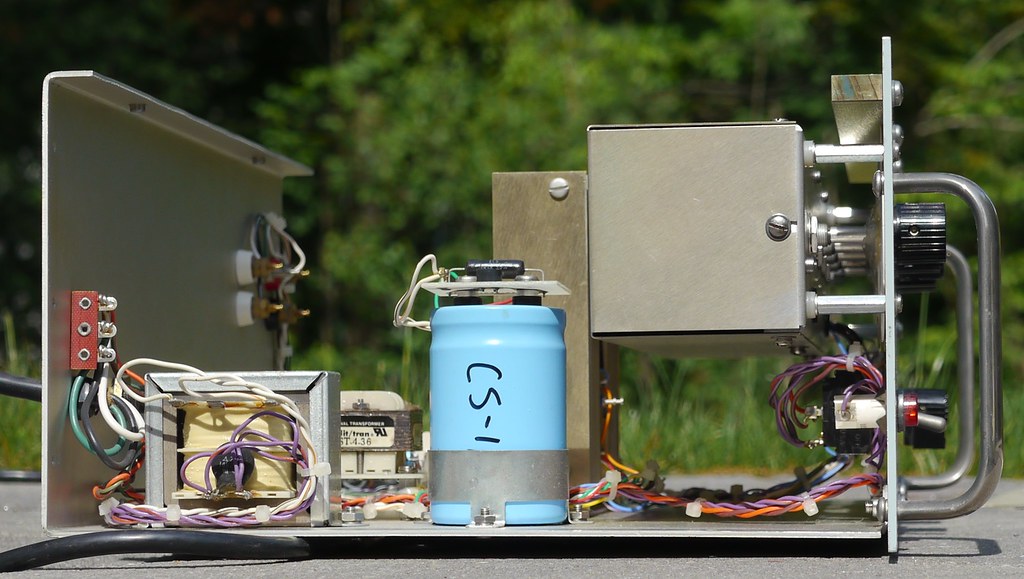
I really like the enclosure that this has, because it's very easy to work with, especially after you take the sides off. You can see the main capacitor here and it's labeled with the model number of the unit. It's a Mallory 250 V unit. Only 85C, but it doesn't really get that hot in the enclosure. It's in the MFD range, but I didn't take it out of it's holder to see what exact value.
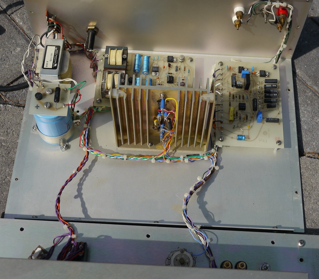
Here I have taken the front panel off to better show off the insides. It comes apart very easily. You can see those two transistors on the large heatsink and the circuitry is built off them from turrets. Was this to keep the leakage down so this unit can get it's 1 uA resolution or just a product of the times? This picture is very useful to see where all the bits of the cable loom go and how nicely they are connected together. The lower transistor is an IRF332 and the upper one is a 2n5250 (I think, my picture isn't very clear)

close up of transistor wiring. I love how bright and festive the colors are. The "crust" is flux residue that I plan to clean off next time I have the alcohol out.
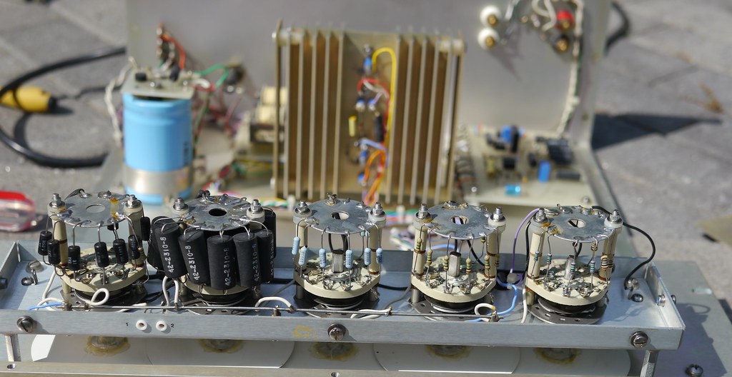
Box of resistors opened! Here you see the resistors connected to the ranging switches. You can also see the digit on the switch is just hot glued to the shaft. A few of the 10 M resistors on the left are different and look newer. Perhaps this was repaired once? You can also see the test points at the lower left here, which can be accessed when the box is closed.
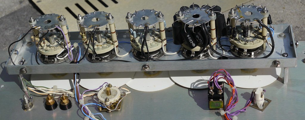
Back of the range resistors. You can also see the outputs on the lower left, the polarity switch in the middle and on the right are the power switch and power lamp. There are only 3 wires going to the resistors. the blue with white stripe, the purple with white stripe and the brown, which is coaxial. The big expensive looking ones are only on the first 2 ranges and the rest are more normal resistors. Maybe the 10 M on the left and 1M next to it for the lowest ranges precision doesn't matter as much as for the higher ranges.
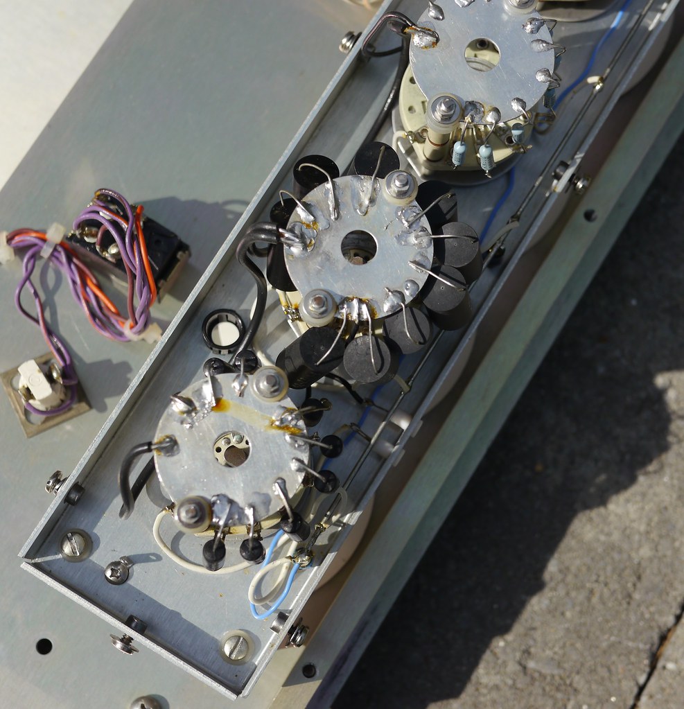
Top of the ranges. You can see how they barely managed to cram those resistors in there, and the soldering work is good to look at. Having soldered to metal, I know how hard it is, so I cut them some slack, but it's not exactly even and they didn't clean off the flux later.
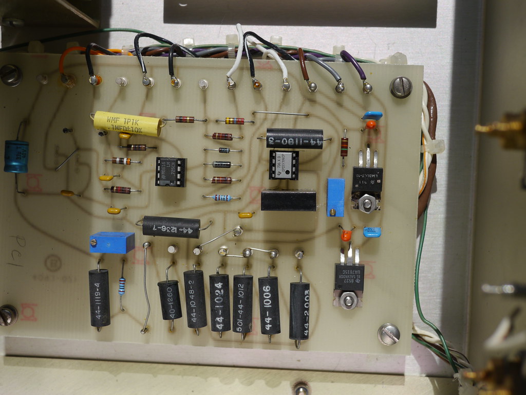
Back to the inside, this is the board I'm making a schematic for now. Since it's a 1 layer PCB it's not hard. I'm still not sure about the component right below the OP07, there is no marking on it at all. Right now the guess is that's a zener diode in a thermal box. I'm still not sure why two of those resistors have been shorted out
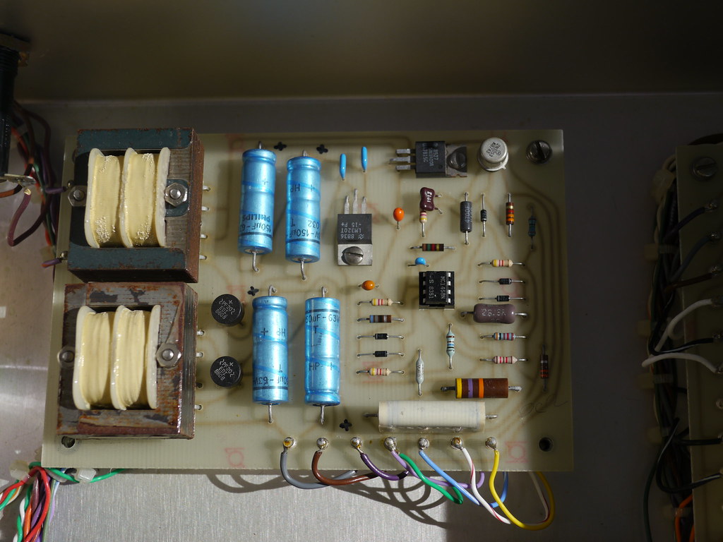
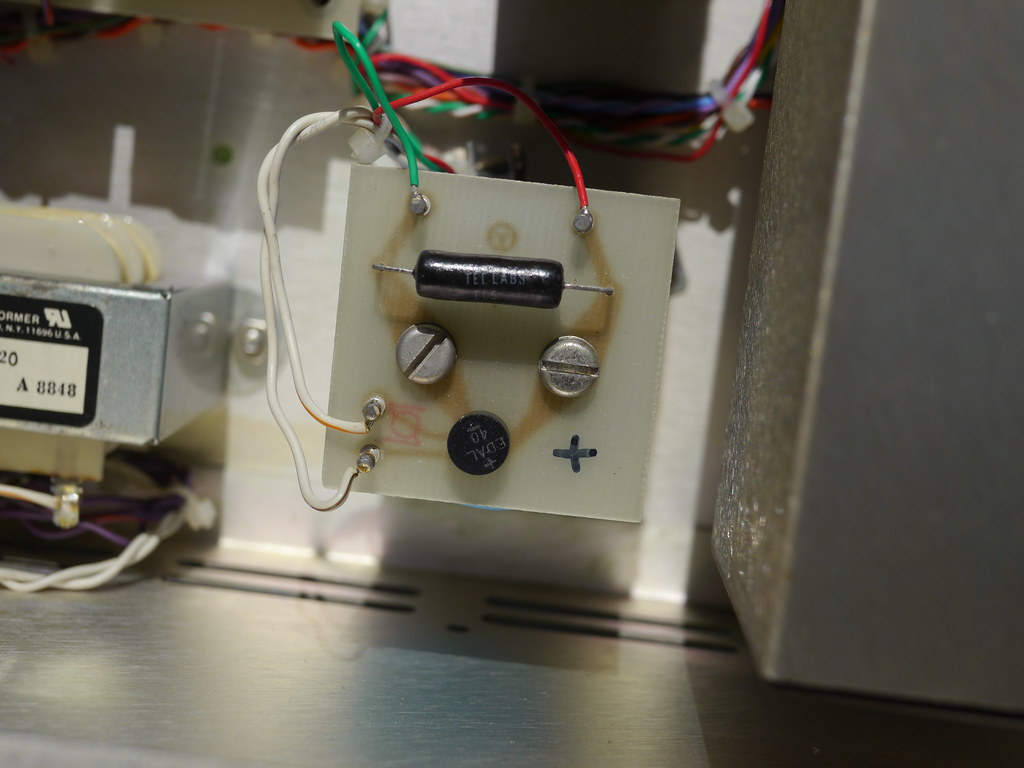
Here's the power supply for the unit. It's pretty high voltage, over 100V. I like how the capacitor polarity is labeled on the PCB by hand. I'll measure what's going on a bit better soon
tm. Yes that is rust on the transformers.
I'll post the schematic and wiring once I get done with it. Let me know here if you have any questions. The full album of photos can be found here.
https://www.flickr.com/photos/dork_vader/albums/72157666604137483/ I have some other devices that I've taken apart and I'll post about them in time. I also have some others that I haven't uploaded to flickr yet. Most of the test equipment is towards the bottom.
I was going to post my kikusui PMC35-2 but the photos are terrible so I will have to reshoot them again. It's a huge pain to take apart though.
Cheers!


