
The ГT906 (GT906) is a germanium power transistor that can block up to 75V. Maximum collector current is 10A. Up to 15W can be dissipated through the package. The temperature of the die must remain below 75°C. The cutoff frequency is 30MHz.
You can´t identify the manufacturer.

The second line could be a date code (1981).
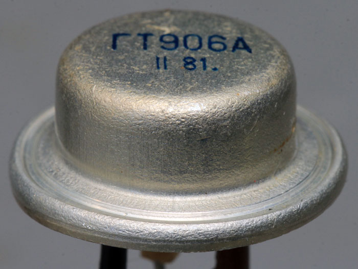

The pin holes looks a little sloppy.

A dry agent.
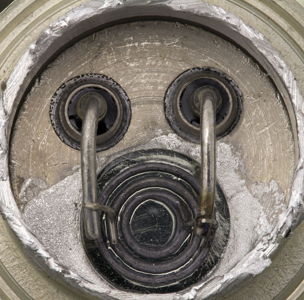

That´s an interesting pin conduct.

The design of the GT906 looks similar to the Philips AU103 (
https://www.richis-lab.de/Bipolar03.htm). The diameter of the germanium disk is round about 6,8mm. There are three solder circles that are connected with the pins.


The inner and the outer ring are connected to the base pin. The ring in the middle is connected to the emitter pin.
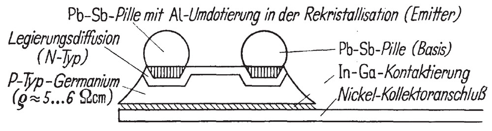
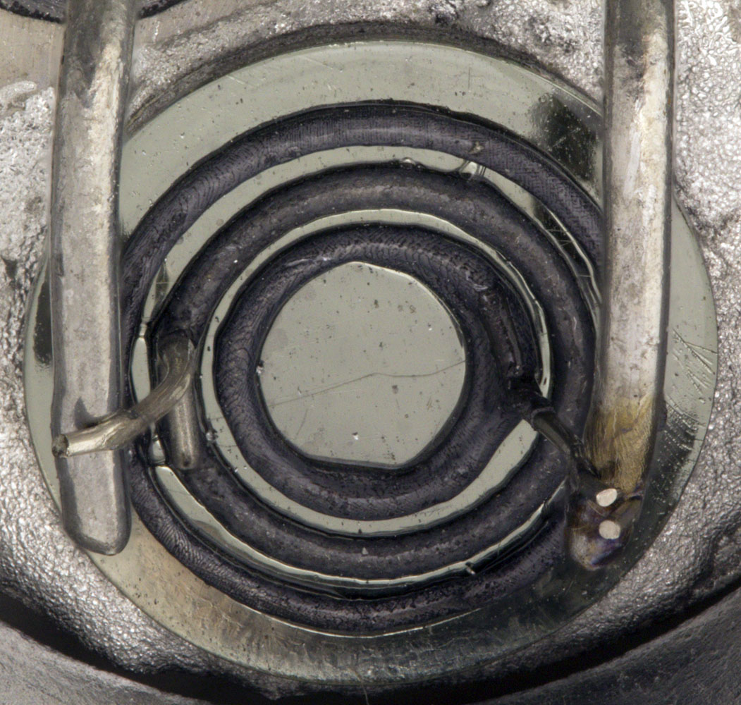
The GT906 is a post-alloy diffused transistor (PADT). The picture above shows how the structures of the transistor probably look like. It is taken from "Einführung in die Physik des Transistors" written by W.W. Gärtner.
You start with a p-doped slice that is the collector. Then you put Pb-Sb on the slice where you want to get a base contact and Pb-Sb-Al where you want to get the emitter contact. After a heat treatment these elements are alloyed with the germanium slice. Since Sb diffuses faster than Al you always have a n-doped layer (Sb) under the p-doped emitter area (Al).

Sometimes PADTs are manufactured in two steps and there is a diffusion process before the alloying. The diffusion brings an initial base layer into the slice. It seems like this was done a lot with HF transistors like the 2N1561 (
https://www.richis-lab.de/Bipolar17.htm).
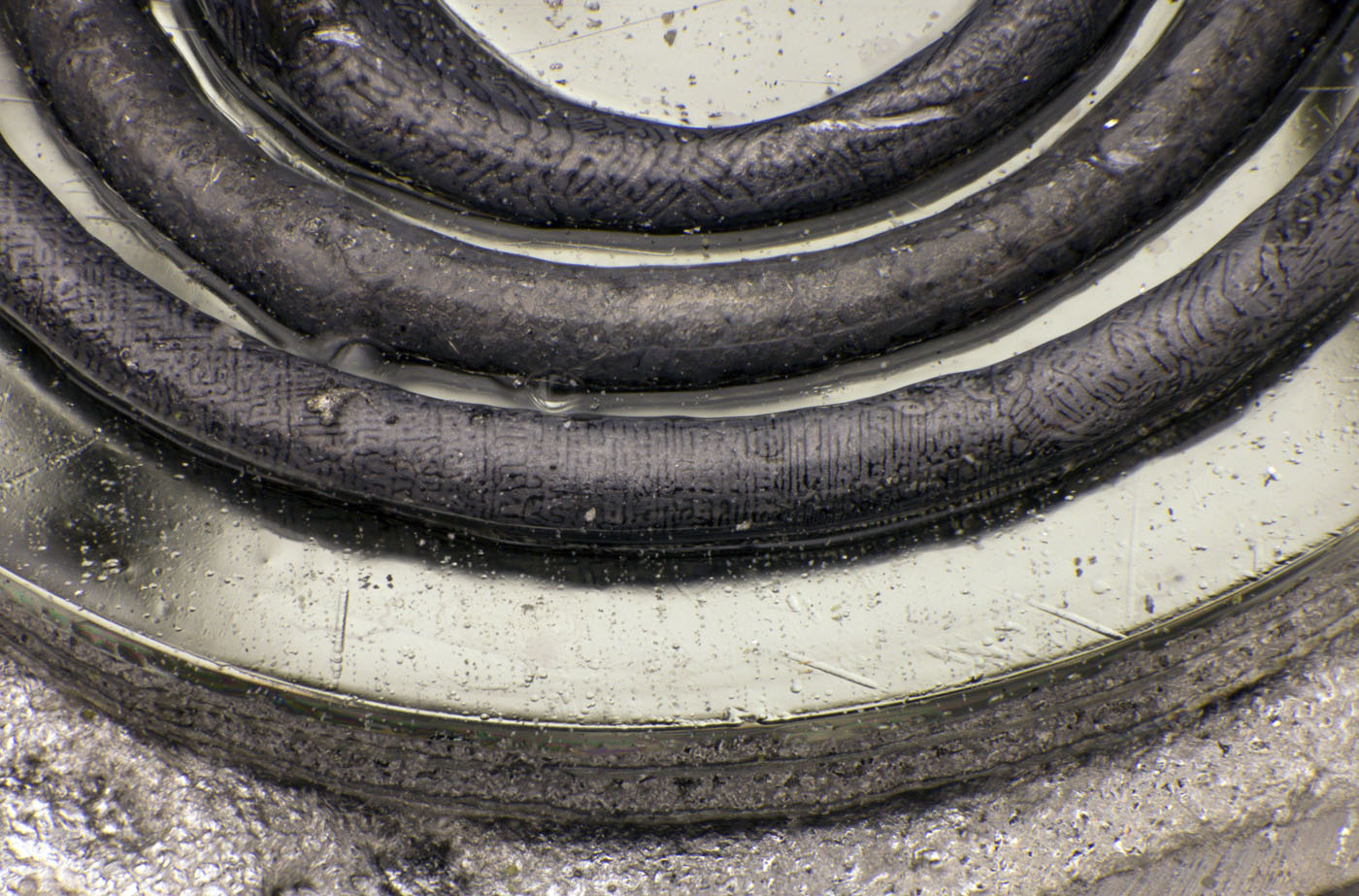
Base and emitter ring have to be located as near as possible to get low resistances to the active area.
You can see the different structures of the rings probably due to the different materials.
Looks like there is a transparent protective coating on top of the die.

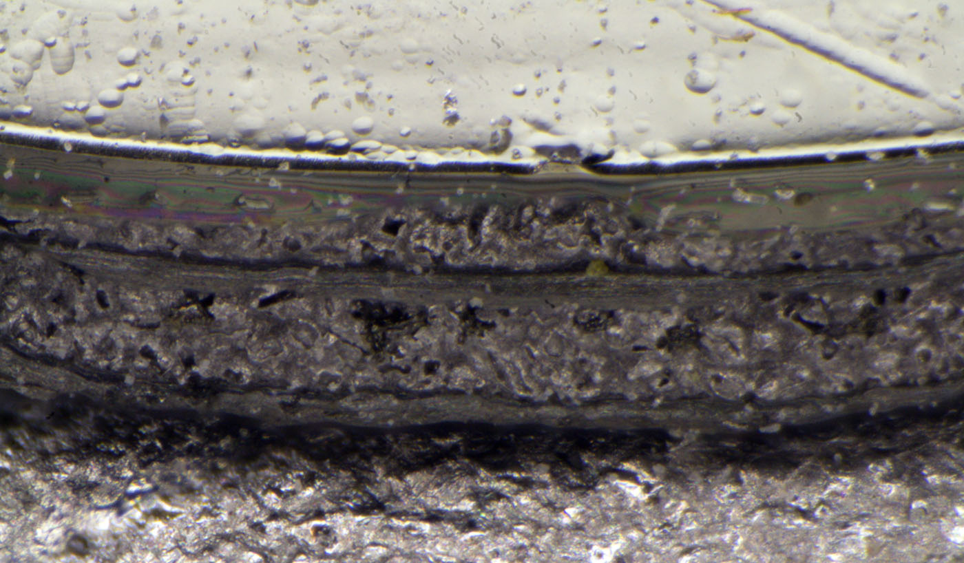
The thickness of the germanium slice is only round about 20µm. It is placed on a carrier with a height of 0.3mm.
The germanium slice must be very thin so the collector resistance doesn´t get too high. If we assume a specific resistance of 5Ωcm as shown in the book above, a diameter of 6,8mm and a thickness of 20µm gives you a path resistance of 28mΩ. At the maximum current of 10A you get 2.8W of power loss in this area!
https://www.richis-lab.de/Bipolar84.htm 
In addition I have updated:
2N1561
https://www.richis-lab.de/Bipolar17.htmAU103
https://www.richis-lab.de/Bipolar03.htm


