Author Topic: Transistors - die pictures  (Read 257098 times)

0 Members and 8 Guests are viewing this topic.

Offline NoopyTopic starter

  • Super Contributor
  • ***
  • Posts: 1895
  • Country: de
    • Richis-Lab
Re: Transistors - die pictures
« Reply #225 on: October 06, 2020, 06:24:56 pm »

I have taken a look into different *44H*-transistors.


D44H11


Decapping was a bit hot...  ::)


D44H8


It seems the D44H8 (specified for lower voltages) is the same as the D44H11. Perhaps ST does some binning and the higher quality is specified for higher voltages...


KSE44H11


On Semi (Fairchild) uses a different structure.
Don´t know why they integrated these holes in the metal layer...  :-//


In the KSE44H11 you can´t find a pn junction. I also wasn´t able to show some light in breakdown mode.
With a closer look at the emitter metal contact we find two steps. One is the contact to the emitter area. Perhaps the second step is the pn-junction. But why did ON hide it under the metal?   :-//


https://www.richis-lab.de/Bipolar21.htm


The Transistors were donated by exe.  :-/O
 
The following users thanked this post: exe, justanothername

Offline exe

  • Supporter
  • ****
  • Posts: 2622
  • Country: nl
  • self-educated hobbyist
Re: Transistors - die pictures
« Reply #226 on: October 06, 2020, 09:07:24 pm »
Niice, although I'm still not sure which one is better :).

Concerning the metal layer over the pn junction, Could it be to spread the heat?
 

Offline NoopyTopic starter

  • Super Contributor
  • ***
  • Posts: 1895
  • Country: de
    • Richis-Lab
Re: Transistors - die pictures
« Reply #227 on: October 06, 2020, 09:13:54 pm »
Concerning the metal layer over the pn junction, Could it be to spread the heat?

In my view that´s unlikely. The metal is only above the boundary of the pn-junction. Most of the junction is underneath the emitter.

Offline NoopyTopic starter

  • Super Contributor
  • ***
  • Posts: 1895
  • Country: de
    • Richis-Lab
Re: Transistors - die pictures
« Reply #228 on: October 19, 2020, 08:05:50 pm »

Do you know the 2N3553?


RCA first sold this Power-HF-Transistor in 1966.
The 2N3553 combines a ft of 500MHz with a continous collector current of 0,33A (1A peak, 40V).


Two bondwires for the emitter and two bondwires for the base. Probably that´s for low inductance and good current distribution.


The 2N3553 uses a multi emitter structure for low base resistance and fast switching.
RCA had this design patented: US3434019A


Lights on!  8)
Breakdown of the base-emitter-junction occurs at -6,5V (datasheet: -4V).
The light is quite uniform. In normal conduction mode an even current distribution is very important. Otherwise a high current in one transistor could cause thermal runaway.
But there is one transistor (center, left side) in which you can see only a line. There has to be an imperfection.  :-/O


More pictures here:
https://www.richis-lab.de/Bipolar22.htm

 :popcorn:
 
The following users thanked this post: Wolfgang, RoGeorge, Miyuki, serg-el

Offline NoopyTopic starter

  • Super Contributor
  • ***
  • Posts: 1895
  • Country: de
    • Richis-Lab
Re: Transistors - die pictures
« Reply #229 on: October 23, 2020, 09:47:35 pm »


Westinghouse 156-043, that´s an old power ransistor!
(40V 15A)


That´s an interesting potting. It seem´s to be clear with some brownish stuff added in the area of the die...  :-//


A hometaxial transistor.  :-+


Base-Emitter-Breakdown!  ;D (1,5A)
It seems that the structures are quite inhomogeneous. The right side of the die shows almost no light.


More pictures here:
https://www.richis-lab.de/Bipolar23.htm

 :-/O
 
The following users thanked this post: exe, SilverSolder, Wolfgang

Offline exe

  • Supporter
  • ****
  • Posts: 2622
  • Country: nl
  • self-educated hobbyist
Re: Transistors - die pictures
« Reply #230 on: October 24, 2020, 09:56:27 am »
That's another brand I've never heard of. Looking in up in wikipedia, it seems they were quite big back in the day, until dissolved in other companies.
 

Offline NoopyTopic starter

  • Super Contributor
  • ***
  • Posts: 1895
  • Country: de
    • Richis-Lab
Re: Transistors - die pictures
« Reply #231 on: October 24, 2020, 10:52:44 am »
Westinghouse is known for old big generators, all kind of old power distribution, nuclear reactors and much more.
But till this one I haven´t seen a Westinghouse transistor too.  8)

Offline NoopyTopic starter

  • Super Contributor
  • ***
  • Posts: 1895
  • Country: de
    • Richis-Lab
Re: Transistors - die pictures
« Reply #232 on: October 28, 2020, 01:35:21 pm »
Let´s look at a big darlington built in the "Gleichrichterwerk Stahnsdorf": SU510
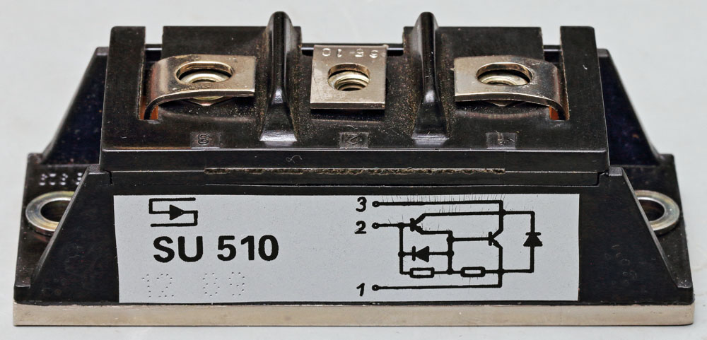


800V / 30A / 250W
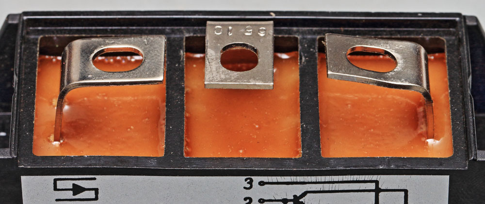


Without screws you can simply slide out the top cover.
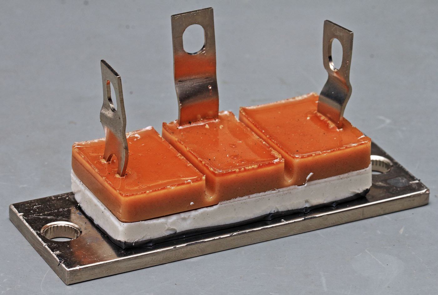


Under the black case there is a white silicone similar to "normal" silicone protecting the semiconductors.
On the bottom there is a thin black layer. I assume the black layer just had to hold the case during assembly and applying the white potting.
On top there is a brownish hard potting. Obviously this material protects the silicone since the top of the case is virtually open.
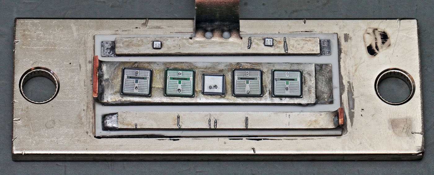


Cutting the metal sheet contacts you can remove the brown part. The silicone potting had to be removed with patience. On thin layers silicone remover can help.
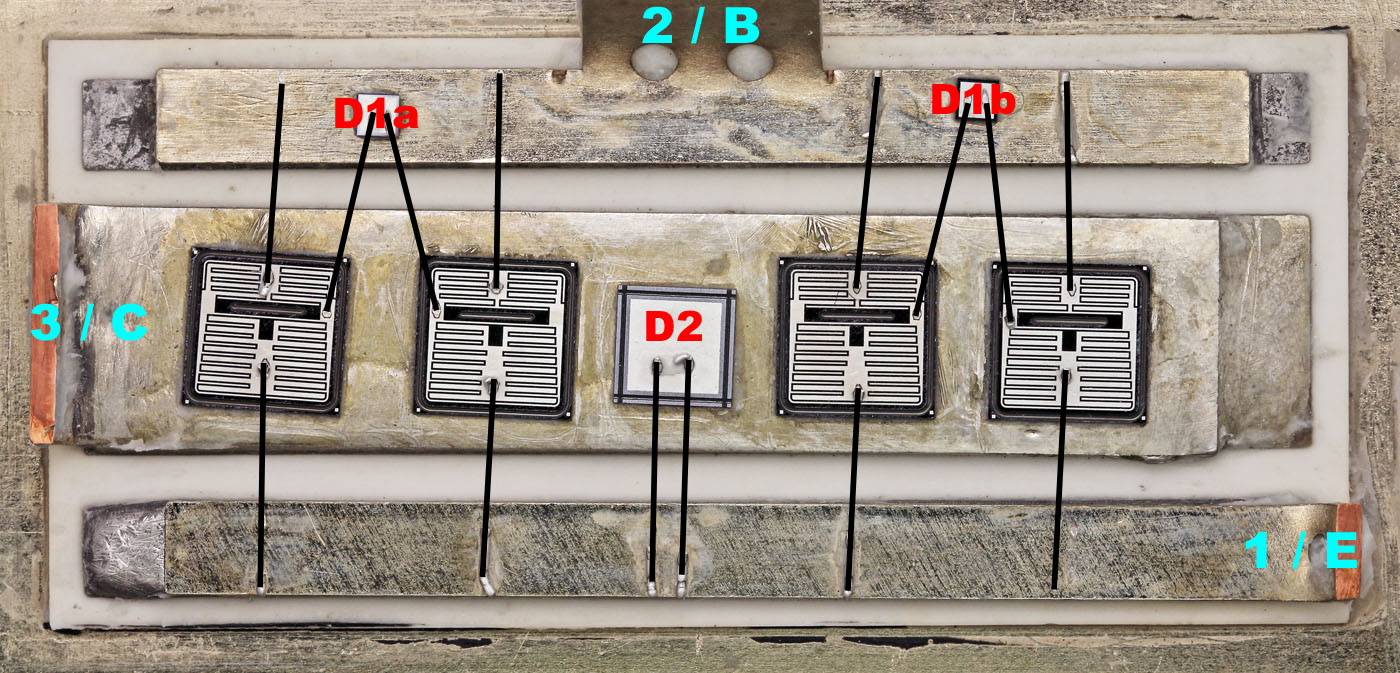


In the package there are four Darlington-Dies and a large freewheeling diode. Two small diodes are connected in parallel to the base emitter junction of the driver transistor for faster switch off.
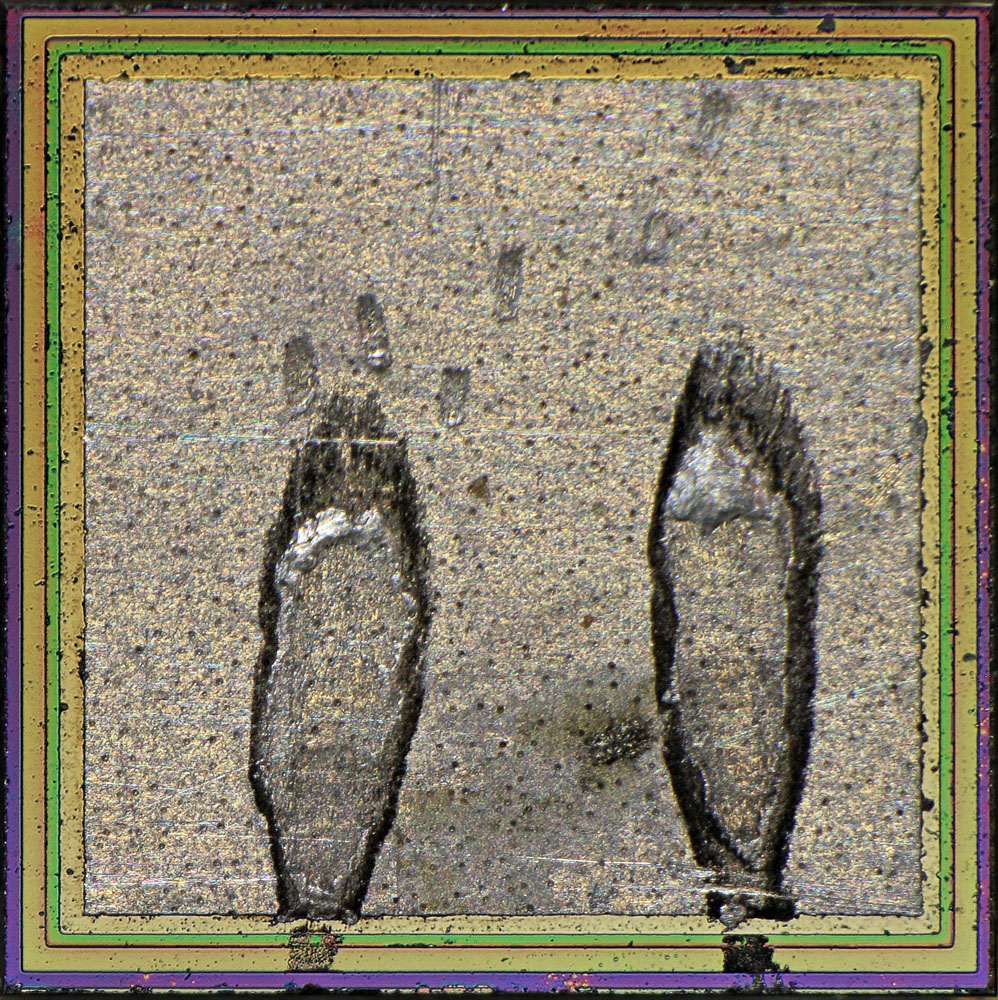


The small diodes own only small structures at the edges because they don´t have to withstand high voltages.
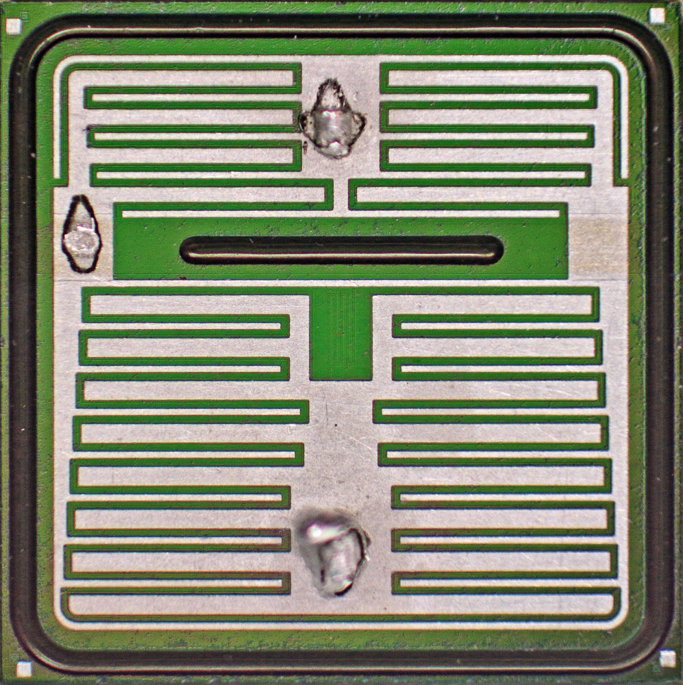
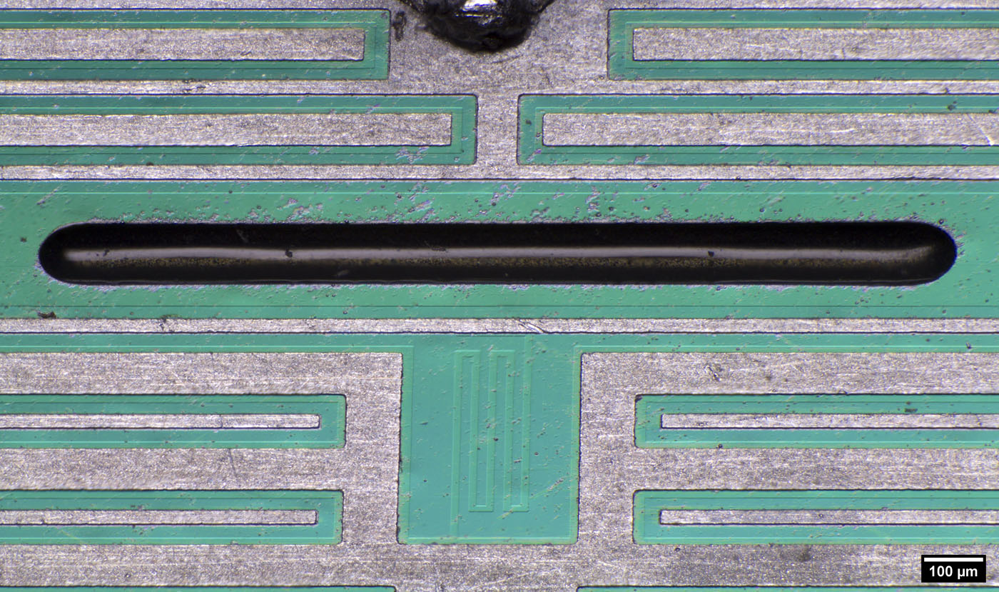


The darlington transistor die is quite interesting. In the upper area there is the driver transistor. In the lower area there is the power transistor. Between these transistors they etched a trench. I wonder what exactly is the purpose of this trench. It somehow has to isolate the two transistors.
In the middle of the die you can see the resistor connected between base and emitter of the power transistor.
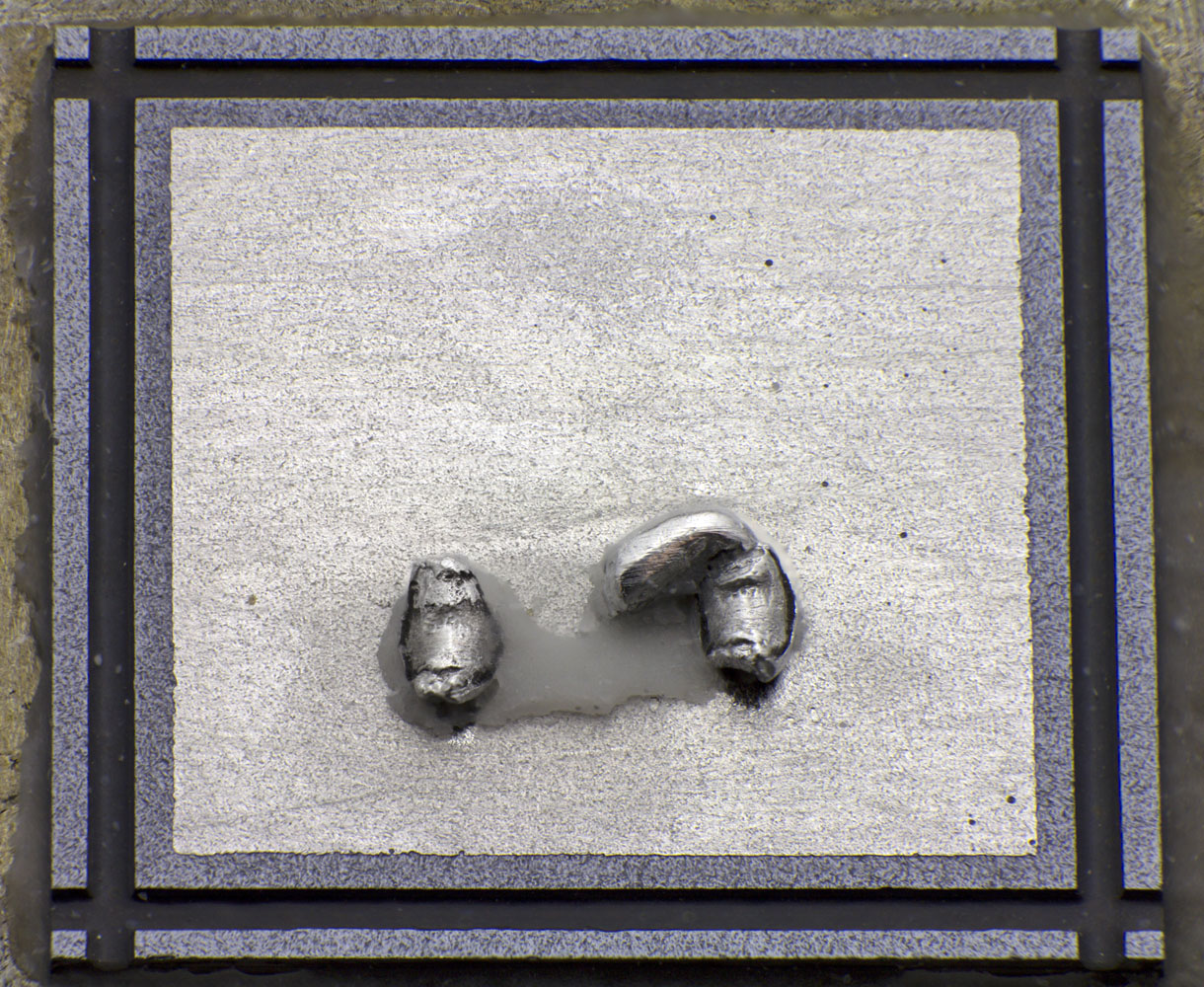


The freewheeling diode has to withstand the full voltage and because of that has etched edges to reduce leakage current.


More pictures here:

https://richis-lab.de/Bipolar24.htm

 :-/O
 
The following users thanked this post: exe, SilverSolder, Miyuki

Offline NoopyTopic starter

  • Super Contributor
  • ***
  • Posts: 1895
  • Country: de
    • Richis-Lab
Re: Transistors - die pictures
« Reply #233 on: November 01, 2020, 06:02:30 pm »


I took a closer look into a Westinghouse 1561-0403 (50V/15A). I wanted to see how similar it is to the 156-043 (40V/15A).


The 1561-0403 also has this yellow-brown potting but here it is more homogenous.
And Westinghouse used some years after the 156-043 a smaller die although the 1561-0403 can withstand higher voltages. Interesting...


The base-emitter breakdown is also very inhomogenous (1A).


https://www.richis-lab.de/Bipolar25.htm

 :-/O
 
The following users thanked this post: exe

Offline NoopyTopic starter

  • Super Contributor
  • ***
  • Posts: 1895
  • Country: de
    • Richis-Lab
Re: Transistors - die pictures
« Reply #234 on: November 06, 2020, 10:46:10 pm »


Have you ever heard of Greaves?  :-//


We find a small modern die in the package.


The transistor is shorted between collector and emitter.


But hey, the base-emitter-junction is good enough for some light (1A)!  ;D


https://www.richis-lab.de/2N3055_12.htm

 :-/O
 
The following users thanked this post: exe

Offline NoopyTopic starter

  • Super Contributor
  • ***
  • Posts: 1895
  • Country: de
    • Richis-Lab
Re: Transistors - die pictures
« Reply #235 on: November 17, 2020, 12:53:25 pm »
Today I have a IGBT for you: IXYS IXGH48N60C3D1


Different packages but same internal construction / dies.


On the left we see the IGBT. On the right we see the freewheeling diode.


The IGBT is 7,2mm x 6,1mm


Potential steering to manage the high voltage.


In the gap between the two metal areas you can spot the traces conducting the gate current under the emitter area.


The freewheeling diode is 6,6mm x 4,2mm.


Probably there is also potential steering but they have put some black stuff on this area.


https://www.richis-lab.de/Bipolar26.htm


By the way I have done some sorting:
Here you can find the bipolar silicon transistors: https://www.richis-lab.de/Transistoren.htm
Here you can find the bipolar germanium transistors: https://www.richis-lab.de/Transistoren_Ge.htm
Here you can find the FETs: https://www.richis-lab.de/Transistoren_FET.htm

 :popcorn:
 
The following users thanked this post: exe, RoGeorge, Miyuki

Offline exe

  • Supporter
  • ****
  • Posts: 2622
  • Country: nl
  • self-educated hobbyist
Re: Transistors - die pictures
« Reply #236 on: November 20, 2020, 12:29:52 pm »
Wow, those igbt and diode are quite large.
 

Offline Miyuki

  • Frequent Contributor
  • **
  • Posts: 907
  • Country: cz
    • Me on youtube
Re: Transistors - die pictures
« Reply #237 on: November 20, 2020, 12:59:06 pm »
Wow, those igbt and diode are quite large.
It must be huge when
IC25 TC = 25°C (Limited by Leads) 75 A

So bond wires are weaker than die itself  >:D
 

Offline NoopyTopic starter

  • Super Contributor
  • ***
  • Posts: 1895
  • Country: de
    • Richis-Lab
Re: Transistors - die pictures
« Reply #238 on: November 20, 2020, 07:09:25 pm »
Wow, those igbt and diode are quite large.
It must be huge when
IC25 TC = 25°C (Limited by Leads) 75 A

So bond wires are weaker than die itself  >:D

Oh yes, current needs silicon area!  :-+ 8)


Let´s take a look at an older transistor again:


Siemens AD148, a Ge-PNP-transistor: 26V, 3,5A, 0,45MHz


I assume this white powder absorbs humidity.


That´s an interesting colour...  :o ;D 8)
Siemens used one plate for base and emitter connection which is cut after production. We have seen that in the Siemens 2N3055 too: https://www.richis-lab.de/2N3055_01.htm


Here you can see the ring electrode connecting the Ge-plate acting as base.
The whole transistor is placed on a socket.
On top of the base you can spot a edged pit with some plating. I assume that´s indium to form the emitter.
The emitter is connected with something like tin.


https://www.richis-lab.de/Bipolar27.htm


 :-/O
 
The following users thanked this post: SilverSolder, RoGeorge, Miyuki

Offline SilverSolder

  • Super Contributor
  • ***
  • Posts: 6126
  • Country: 00
Re: Transistors - die pictures
« Reply #239 on: November 20, 2020, 08:27:31 pm »

Some of these pictures are quite beautiful and wouldn't look out of place at an art exhibition, LOL!  :D
 

Offline NoopyTopic starter

  • Super Contributor
  • ***
  • Posts: 1895
  • Country: de
    • Richis-Lab
Re: Transistors - die pictures
« Reply #240 on: November 21, 2020, 06:08:29 am »

Some of these pictures are quite beautiful and wouldn't look out of place at an art exhibition, LOL!  :D

Thanks!  8)
Till know I only have a calender: https://www.meinbildkalender.de/richis-lab
Next "merchandise project" is a LTZ1000 coffee pot.  :D
 
The following users thanked this post: SilverSolder, sandalcandal

Offline floobydust

  • Super Contributor
  • ***
  • Posts: 7492
  • Country: ca
Re: Transistors - die pictures
« Reply #241 on: November 21, 2020, 07:32:32 am »
Apparently tin whiskers are a problem with old germanium transistors, causing short circuits.
NASA failure analysis of vintage radio transistors OC170 and AF114: https://nepp.nasa.gov/whisker/anecdote/af114-transistor/2005-Brusse-tin-whiskers-AF114-transistors.pdf
 
The following users thanked this post: HB9EVI, Noopy

Offline NoopyTopic starter

  • Super Contributor
  • ***
  • Posts: 1895
  • Country: de
    • Richis-Lab
Re: Transistors - die pictures
« Reply #242 on: November 21, 2020, 08:27:02 am »
Thanks for the hint!   :-+
I will take a closer look at the next germanium transistor. Would be nice to take pictures of some whiskers!  :-/O

Offline NoopyTopic starter

  • Super Contributor
  • ***
  • Posts: 1895
  • Country: de
    • Richis-Lab
Re: Transistors - die pictures
« Reply #243 on: November 25, 2020, 07:37:29 am »
Today I have a Motorola 2N2081 for you:


Germanium-PNP-Powertransistor: 45V, 15A, 170W (@25°C), but a quite low ft of 5kHz...  ???


The 2N2081 has an additional base contact in the middle of the die like the AU103 (https://www.richis-lab.de/Bipolar03.htm).


Nice!  8)


Some more pictures here:

https://www.richis-lab.de/Bipolar28.htm

 :-/O
 
The following users thanked this post: SilverSolder, Wolfgang, RoGeorge

Offline exe

  • Supporter
  • ****
  • Posts: 2622
  • Country: nl
  • self-educated hobbyist
Re: Transistors - die pictures
« Reply #244 on: November 25, 2020, 08:14:39 am »
ft of 5kHz...

That's the slowest transistor I've seen! I see a plastic cover on collector (?) pin. Did it come in original packaging?
 

Offline NoopyTopic starter

  • Super Contributor
  • ***
  • Posts: 1895
  • Country: de
    • Richis-Lab
Re: Transistors - die pictures
« Reply #245 on: November 25, 2020, 08:39:05 am »
The small pin is for locating base and emitter and holding the transistor in place while tightening the nut.
The plastic cap ensures insulation to the heatsink. You put something like mica under the transistor but the pin needs some extra insulation.

The datasheet states min 5kHz. But nevertheless that´s quite low.
I noticed that in contrast the AU107, also a Ge-Powertransistor, has a quite high ft of 10MHz.
Perhaps the 2N2081 has a lower doping level reducing it´s speed. The datasheet states a quite high maximum die temperature of 110°C. For the AU107 you find 90°C. Perhaps that was the tradeoff.  :-//

Offline Miyuki

  • Frequent Contributor
  • **
  • Posts: 907
  • Country: cz
    • Me on youtube
Re: Transistors - die pictures
« Reply #246 on: November 25, 2020, 09:35:59 am »
Why did they use a whole round crystal for transistors back then?
Is it some property of germanium that it can't be processed like silicon on bigger crystal and then cut to dies or just wasn't the technology to produce bigger crystal back then?
 

Offline NoopyTopic starter

  • Super Contributor
  • ***
  • Posts: 1895
  • Country: de
    • Richis-Lab
Re: Transistors - die pictures
« Reply #247 on: November 25, 2020, 12:40:54 pm »
Sorry, I´m no expert regarding the manufacturing of these old transistors.
Perhaps someone else knows more?

PS: First appearance of the 2N2018 was 1961 as far as I was able to trace it back.

Online RoGeorge

  • Super Contributor
  • ***
  • Posts: 6775
  • Country: ro
Re: Transistors - die pictures
« Reply #248 on: November 25, 2020, 03:25:04 pm »
Why did they use a whole round crystal for transistors back then?
Is it some property of germanium that it can't be processed like silicon on bigger crystal and then cut to dies or just wasn't the technology to produce bigger crystal back then?

I'm not an expert either, but recently bumped into this documentary about the beginning of the semiconductors technology (this one is about Japan).  There are four parts, and the first one is especially about Ge transistors.
https://www.eevblog.com/forum/chat/fun-for-nerds/msg3297026/#msg3297026

It will not explicitly answer your questions, but will let you make an idea about the zeitgeist of the electronic industry back then.
 
The following users thanked this post: Miyuki

Offline Miyuki

  • Frequent Contributor
  • **
  • Posts: 907
  • Country: cz
    • Me on youtube
Re: Transistors - die pictures
« Reply #249 on: November 27, 2020, 11:58:22 am »
It will not explicitly answer your questions, but will let you make an idea about the zeitgeist of the electronic industry back then.
It kinda explains it
They are Alloy transistor
So they are manufactured this way and size, not cut after manufacture
Interesting


Share me

Digg  Facebook  SlashDot  Delicious  Technorati  Twitter  Google  Yahoo
Smf