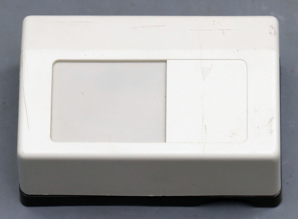
The IR 6 is a passive infrared motion detector from Telenorma. It requires a supply voltage between 10,5V and 15V. In addition to the alarm output, the IR 6 offers tamper protection, where a control loop is interrupted when you open the housing. On the front side there is only an inconspicuous white window transparent to infrared radiation.
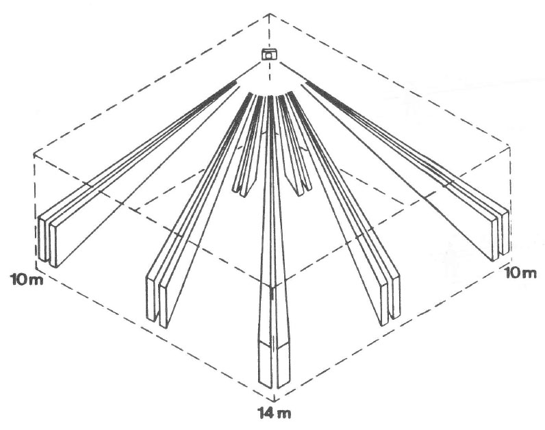
The datasheet shows the detection ranges of the sensor. Five areas extend in the horizontal plane over an opening angle of 90°. The range depends on the angle at which the sensor is mounted on the wall and is up to 14m. At close range, the IR 6 has two additional detection zones.
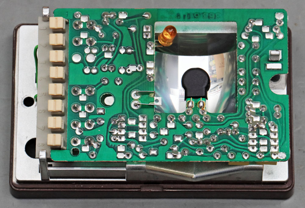
If you remove the cover, you can see the back of a circuit board. The module has been rotated by 180° here. The contact strip is on the left, and a window on the right provides an entry point for infrared radiation. The tamper protection is located in between. A pin fixed in the cover presses there through a hole in the board onto a metal part which closes the loop of the tamper protection.
The orange LED is a so-called walk test indicator. According to the datasheet, it is not visible through the housing, but can also be unplugged. This ensures that no unauthorized person can test the detection range.
Infrared sensors for motion detectors usually offer very few, usually only two elements. The desired resolution over a large area is achieved using Fresnel lenses or concave mirrors. These optical elements ensure that the irradiation on the sensor changes relatively strongly, even if only a small heat source moves through the room.
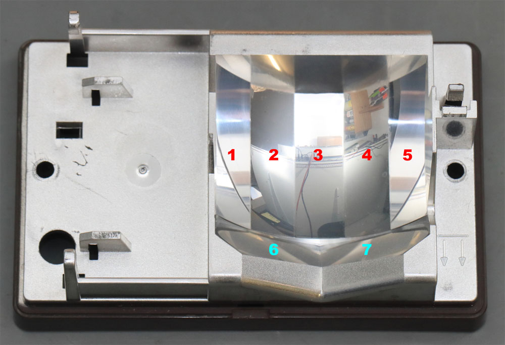
If the circuit board is removed, the concave mirror becomes visible, which in the case of IR 6 directs the incoming infrared radiation to the sensor and thus defines the detection areas. Areas 1-5 are the more far-reaching zones. Surfaces 6 and 7 collect the infrared radiation from the near range.
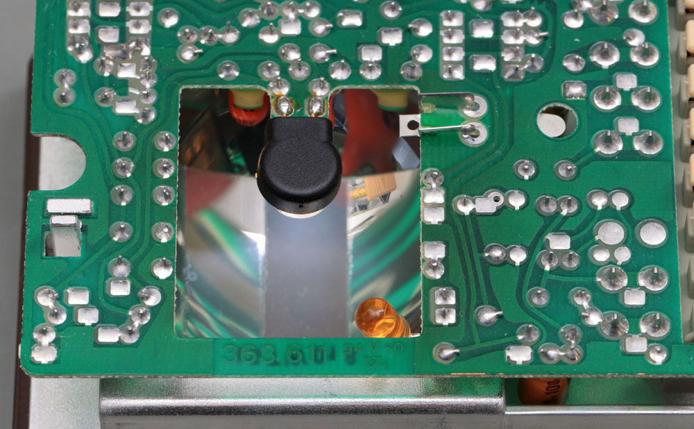
Turned by 180° again, the transition from the wide-range to the close-range reflectors can be clearly seen through the cutout in the pcb. The actual sensor is located under the black element.
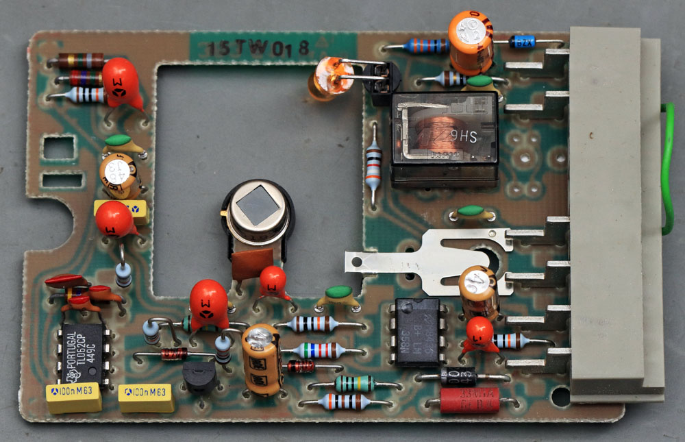
The circuit is not too complex. Usually the signals of the sensor are actively filtered and amplified. Approximately in the center you can see the metal element of the tamper protection and above it the relay that switches the output of the motion detector.
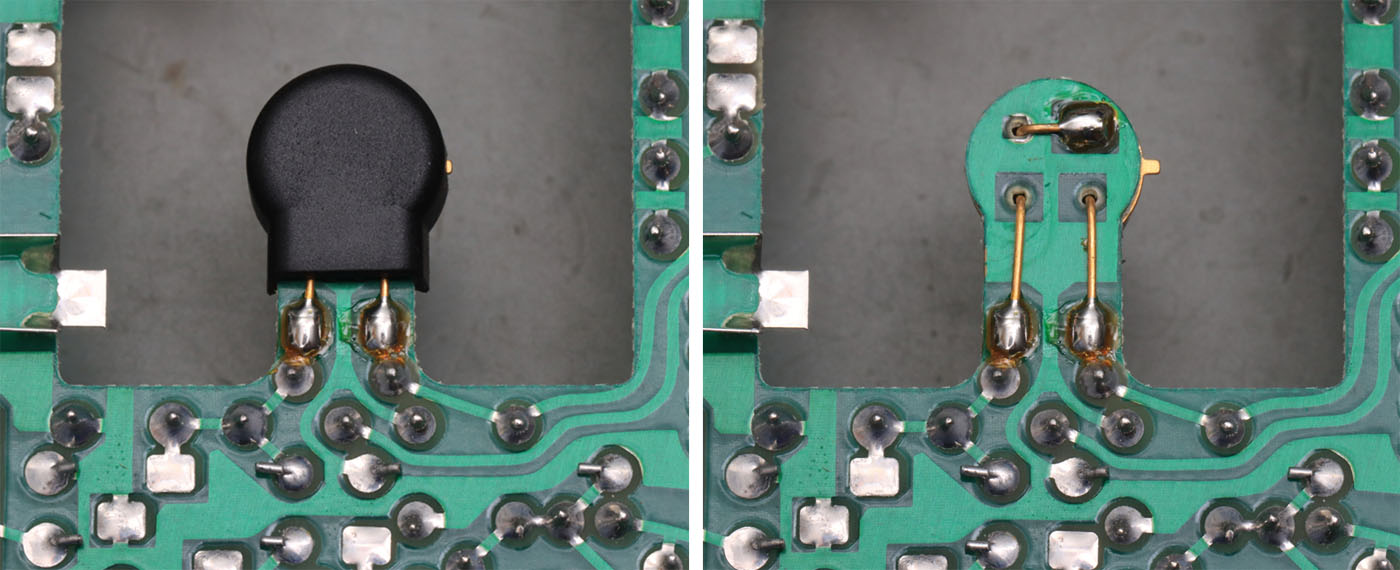
The sensor is covered with a plastic element on the back. Perhaps this ensures that no infrared radiation falls on the pins and generates inhomogeneous heating. Such sensors are extremely sensitive and it is quite conceivable that an inhomogeneous heating of the pins already generates a problematic interference signal.
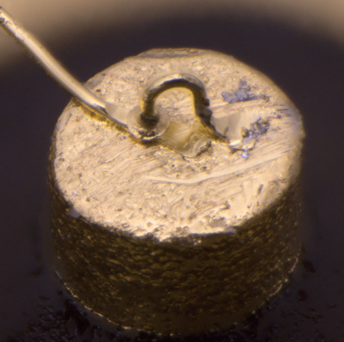
The sensor lies directly on the circuit board. However, you must not heat the sensor elements too much. The datasheet recommends to leave the pins at least 6,35mm long. This explains why the pins are bent downwards and soldered further away of the sensor.
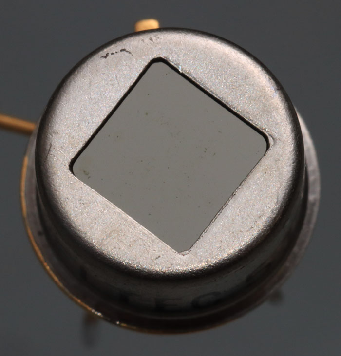
On the front side there is a square window with a filter element.
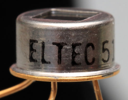
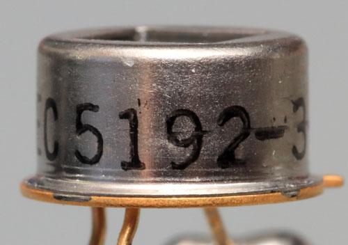
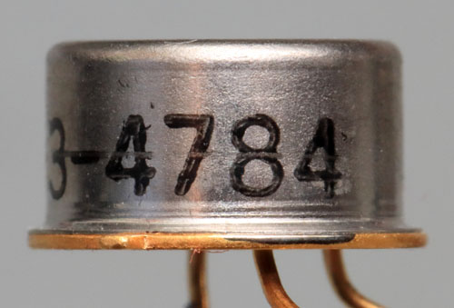
The labeling on the side shows that it is the Dual IR detector 5192 from Eltec. The number 3 behind the designation shows which filter is located in front of the sensor. 3 stands for the silicon filter, which allows wavelengths between 6µm and 25µm to pass. A total of 35 different filters are available. 4784 seems to be a date code.
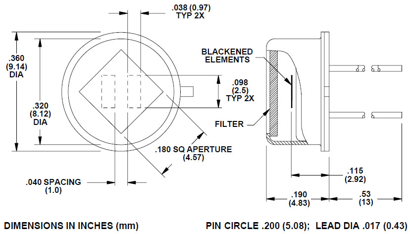
The datasheet shows that there are two sensor elements in the housing.
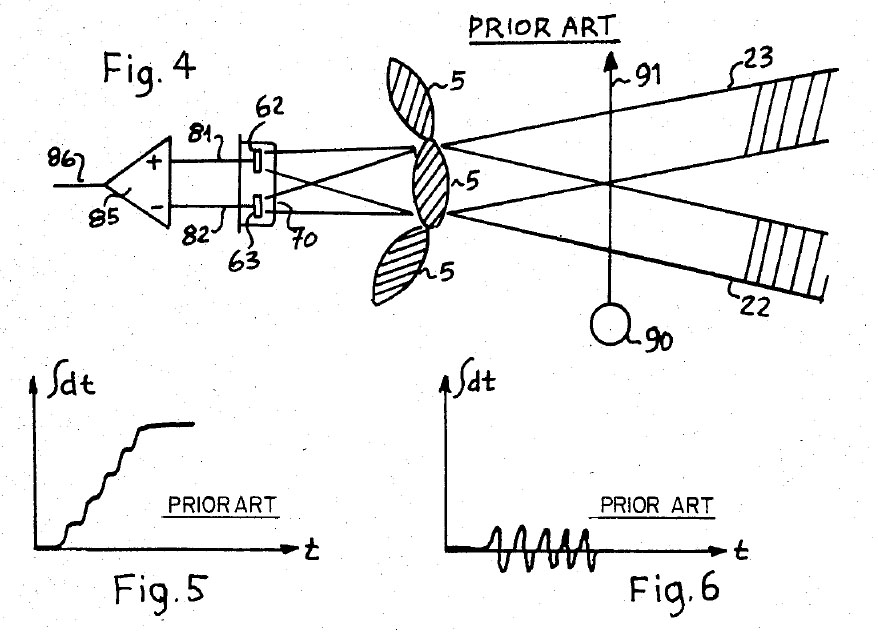
In the datasheet, reference is made to patent US4523095, whose illustrations make it easier to understand how the sensor works. If only a single pyroelectric element were used as a sensor, a warm body in the detection range would just cause the output signal to increase (Fig. 5).
In contrast, the arrangement and interconnection of two pyroelectric elements and the evaluation via a differential amplifier results in an oscillating signal when passing through the detection areas (Fig. 6). This signal is easier to evaluate.
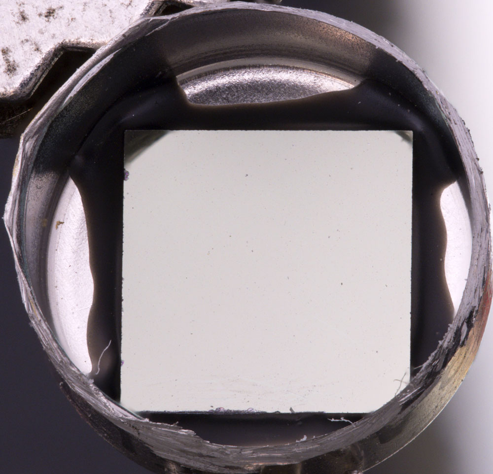
If you open the housing, you can take a look at the glued-in filter element.
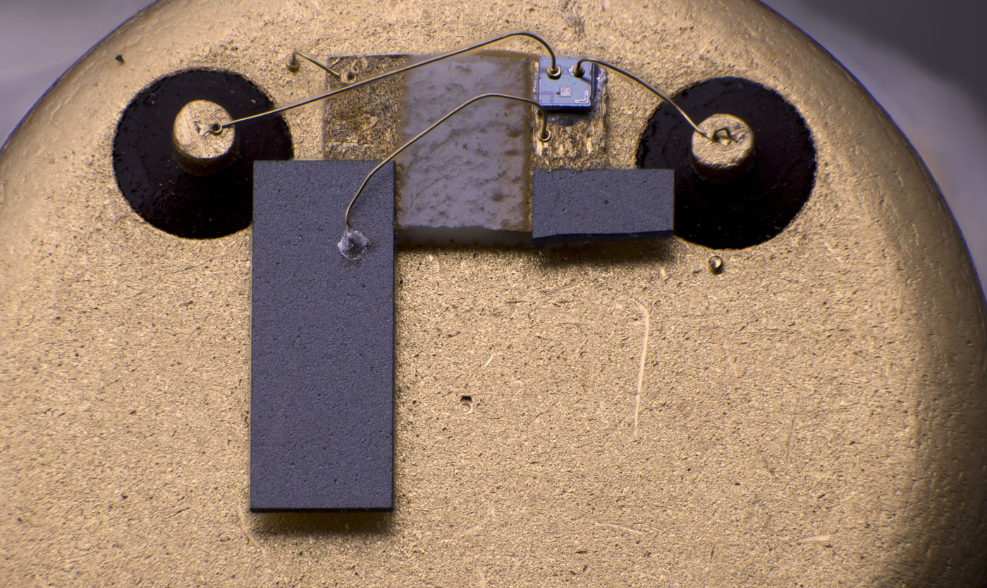
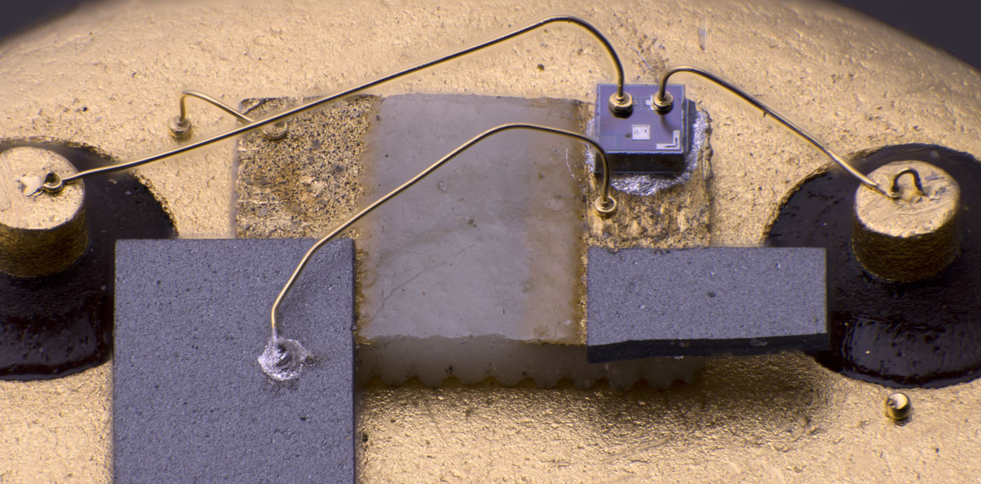
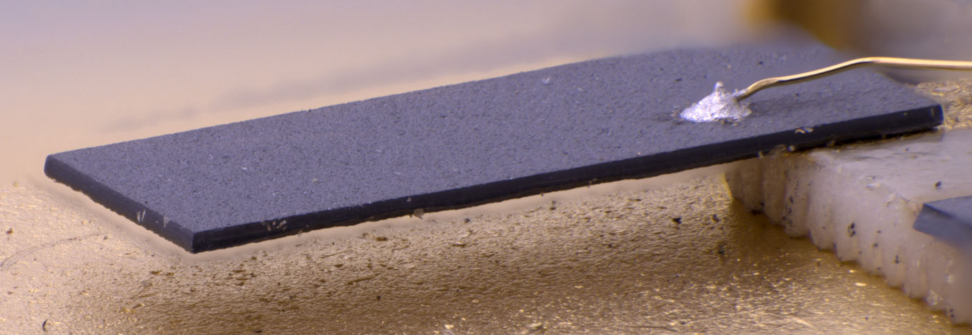
The two pyroelectric elements are mounted on a ceramic carrier. It can be seen that the right element is broken off. The damage could have occurred when opening the case. However, the module in question was discarded because its functionality was unreliable. This suggests that the element had already broken off before.
So-called security bonds were used on the connecting pins. A ball bond is supposed to secure the wedge bond.
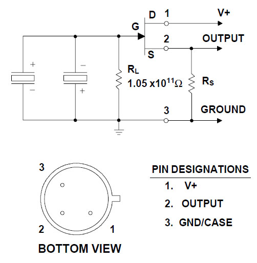
The datasheet shows how the sensor works. The two pyroelectric elements are connected antiparallel and are guided to the gate of a JFET. This interconnection ensures that when an infrared beam changes from one element to the other, the polarity of the signal is reversed. The JFET represents the differential amplifier shown in the patent above. The value of the resistor R_L is extremely high at 105GΩ. Such a high value is necessary because the pyroelectric elements have a very high internal resistance.
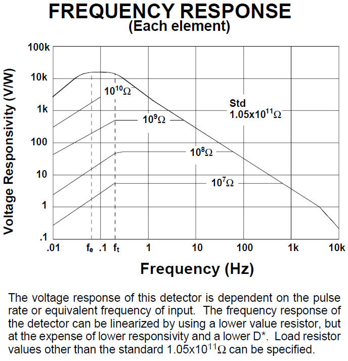
It seems that the sensor can be obtained with lower resistance values. Since R_L discharges the capacity of the sensor, a lower value has a positive effect on the bandwidth. At the same time, however, the sensitivity is reduced.
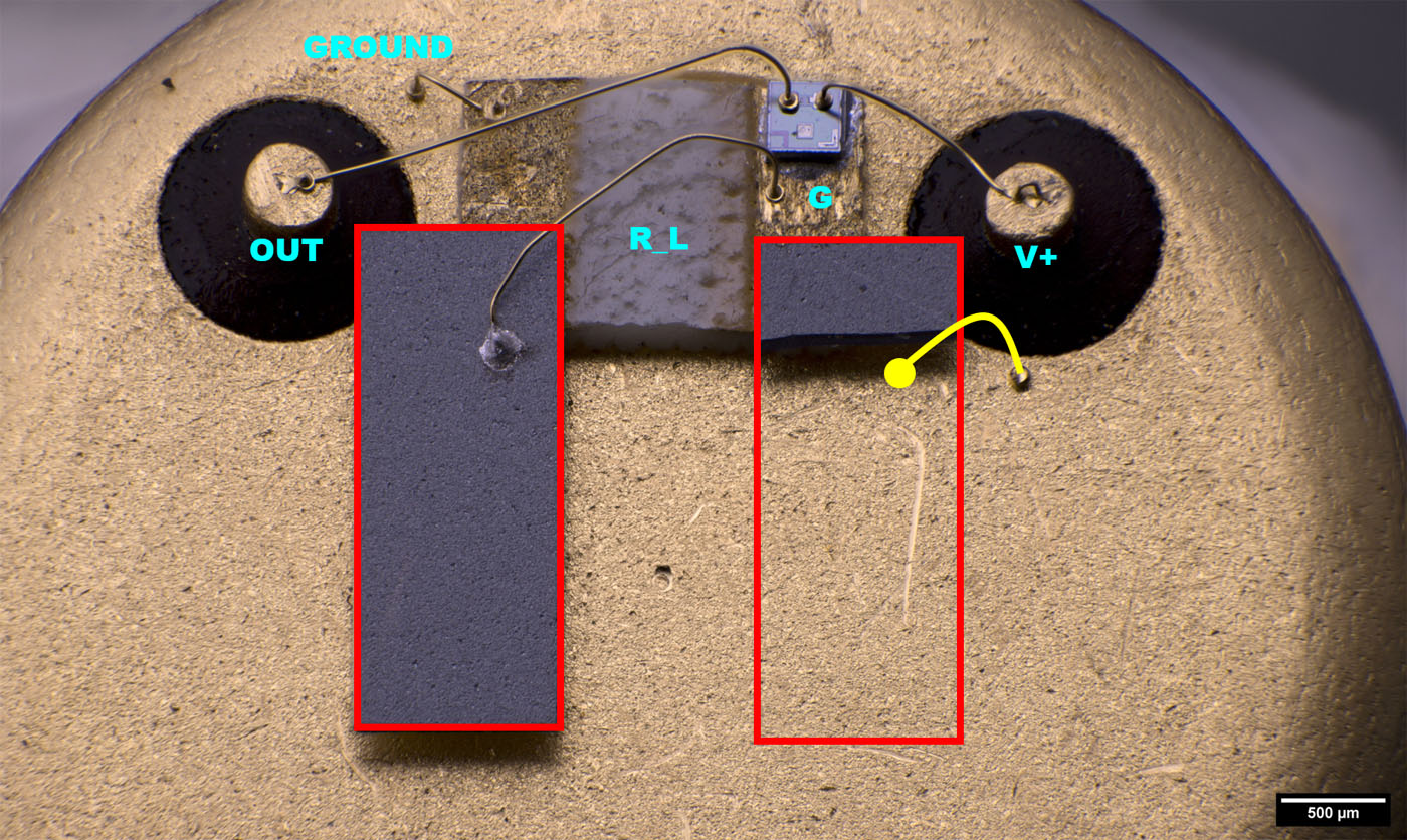
With the background of the operation one can interpret and extrapolate the structures. On the left pyroelectric element, the top is connected to the gate of the JFET. On the right element, the bottom side is directly connected to the gate potential due to the attachment. It can be assumed that the top was connected to the rest of the ball bond on the right of the element (yellow). The extremely high resistance thick film resistor is applied to the ceramic support between the gold contacts.
The significance of the imprint between the thermoelectric elements remains open. It does not appear to be a proper wedge bond. It also lacks the security bond. This suggests that it was not a functional element. Perhaps it is a remnant of the manufacturing process.
Pyroelectric elements can be manufactured from different materials. On Eltec's website, only lithium tantalate is ever mentioned.
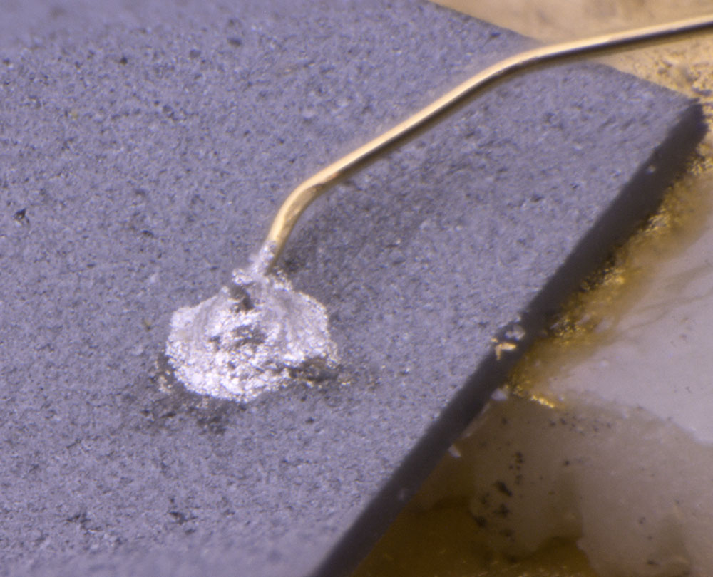
Since it was not possible to bond on the pyroelectric material, the bondwire was soldered.
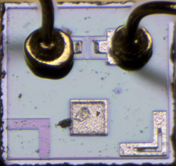
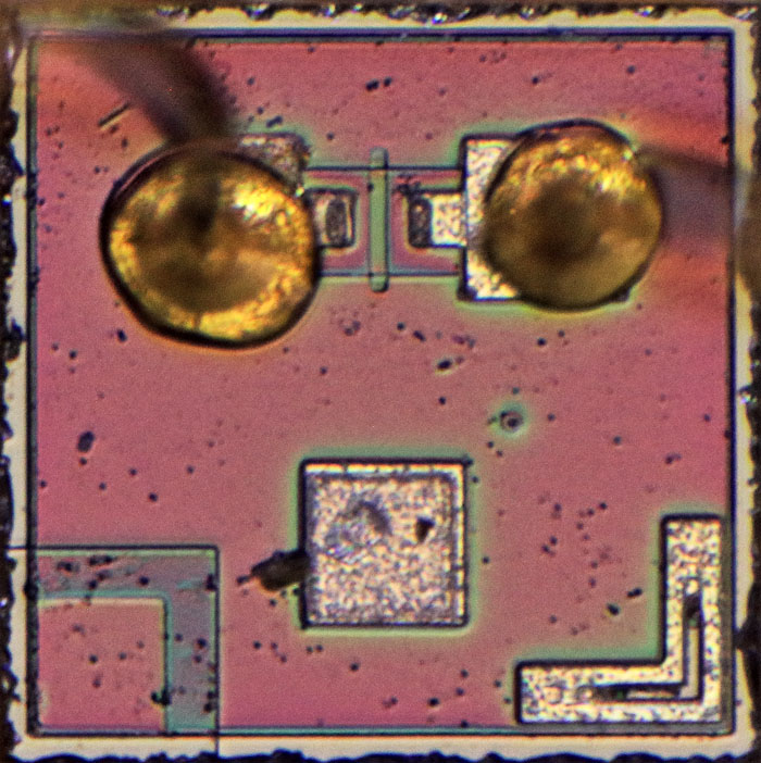
The edge length of the JFET is 0,35mm. The mode of operation can be seen clearly. The two adjacent bondpads contact a wide n-doped strip, which is located in a p-doped area. A thin p-doped strip is deposited on the wide strip, forming an n-doped channel surrounded by p-doped regions over its complete circumference.
Inside the sensor, the gate potential is supplied from below through the substrate. The free bondpad in the lower area offers the possibility to supply the gate potential alternatively via a bondwire.
https://www.richis-lab.de/Opto18.htm 


