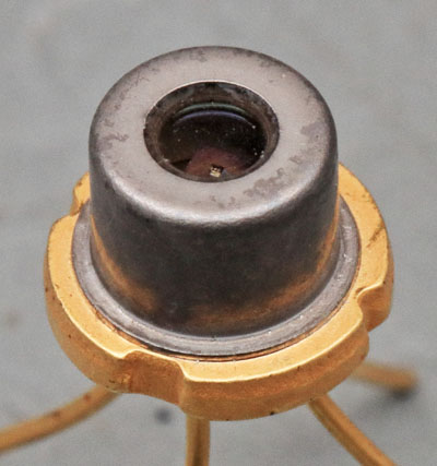
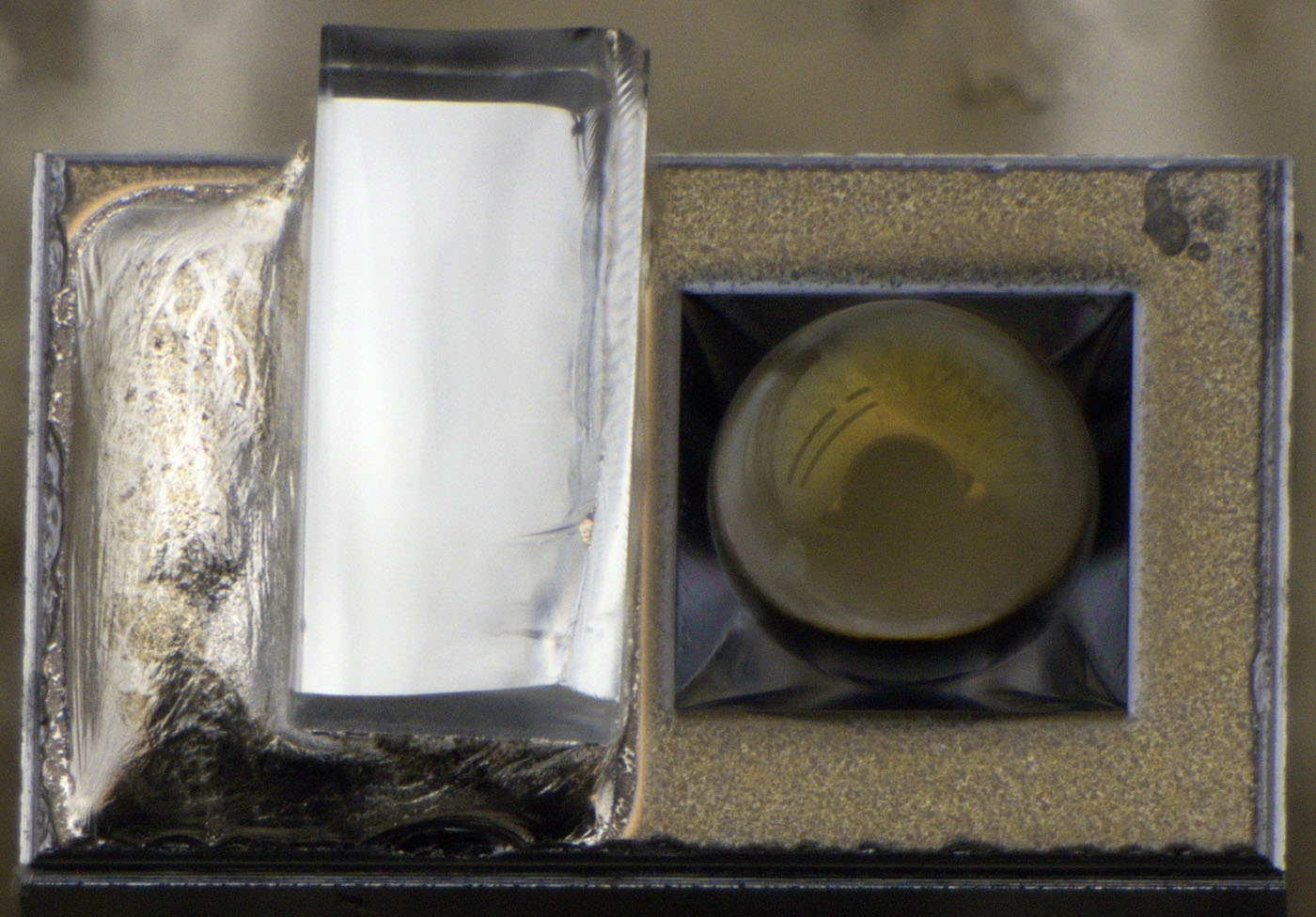
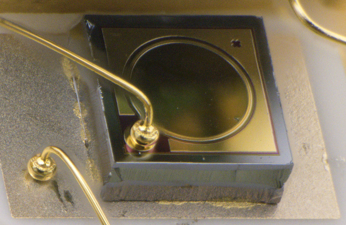
Here you can see a laser module manufactured by Siemens. It is designed to couple a light output of up to 10mW with a wavelength of 1330nm into a glass fiber.
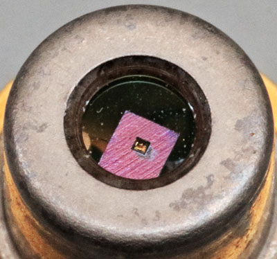
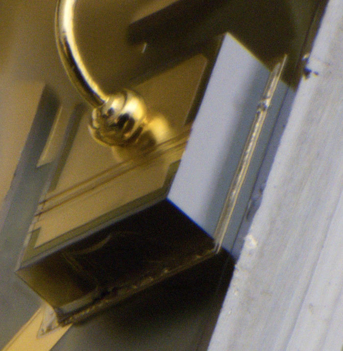
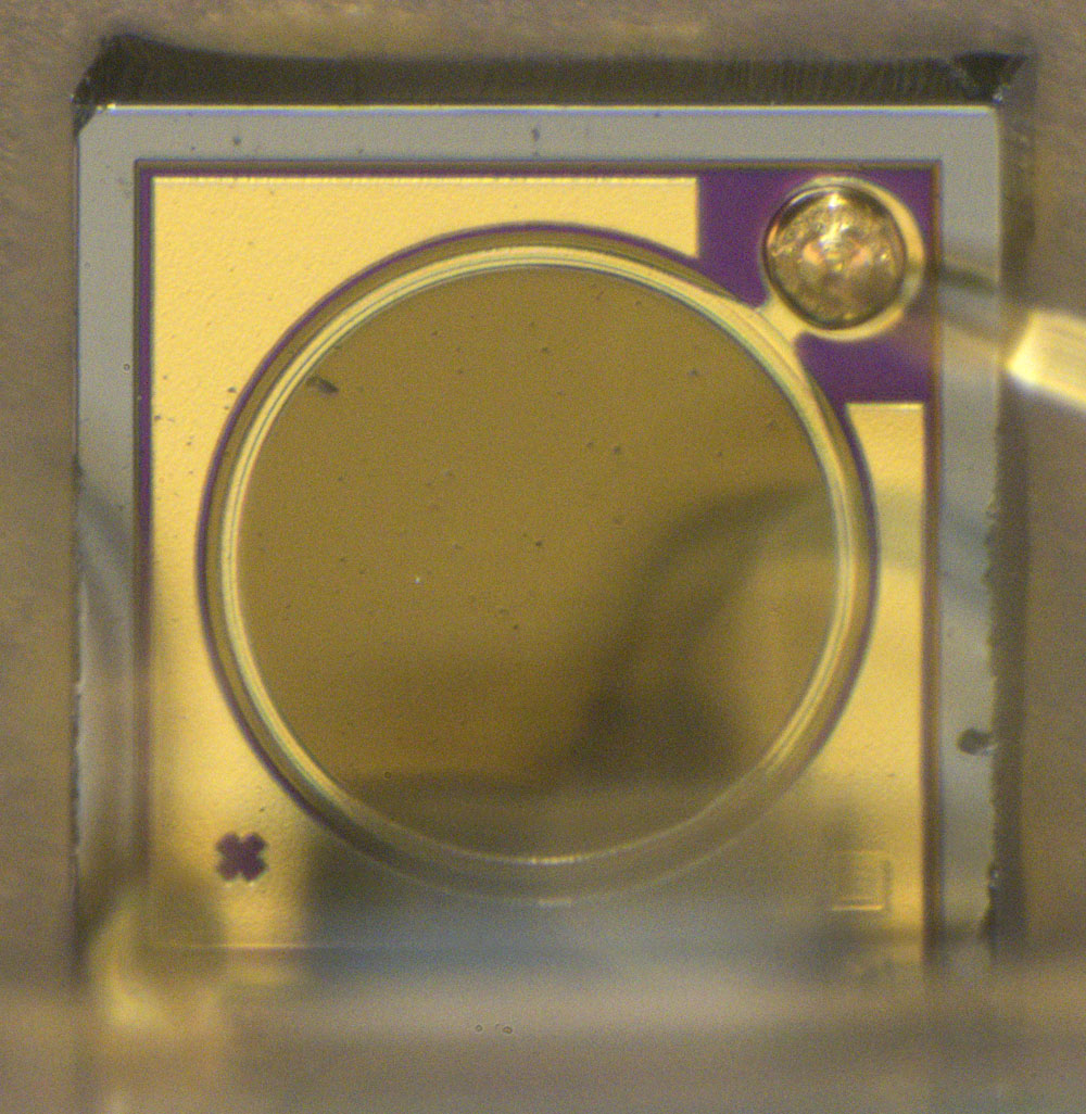
The optical window allows a view inside the package. The structures that can be seen there appear unusual for a laser diode at first glance.
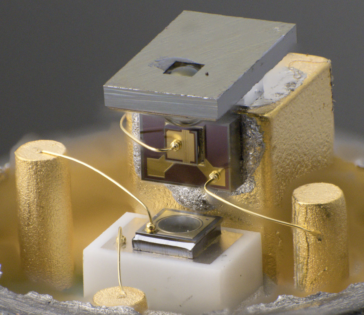
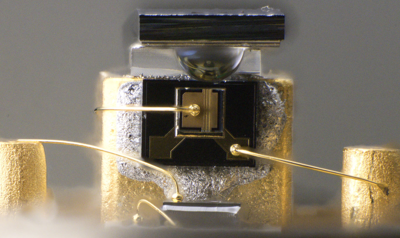
If you open the package, it becomes clear what the top element is. The strip is a carrier for a lens that improves the coupling of the laser light into the glass fiber. A similar element is connected directly to the glass fiber in the IR-LED VQ130 (
https://www.richis-lab.de/Opto16.htm#Linse). The actual laser diode is located under the lens and a photodiode is placed underneath, which makes it possible to determine the current light output. In contrast to the low-cost laser module (
https://www.richis-lab.de/Opto20.htm), the photodiode is insulated from the housing with a ceramic carrier.
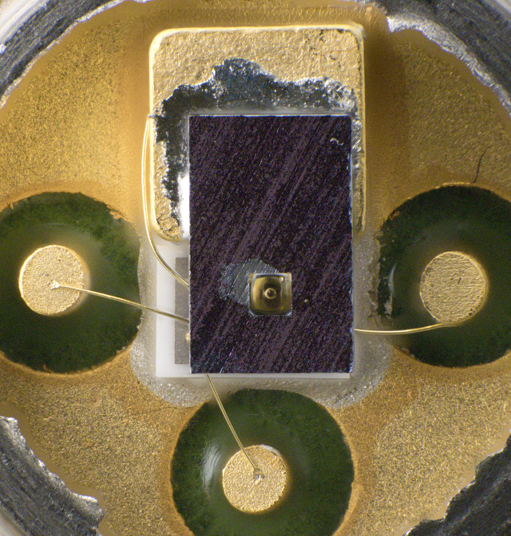
The carrier of the lens appears to be made of silicon. The square through which the laser beam emerges has an edge length of 0,27 mm.
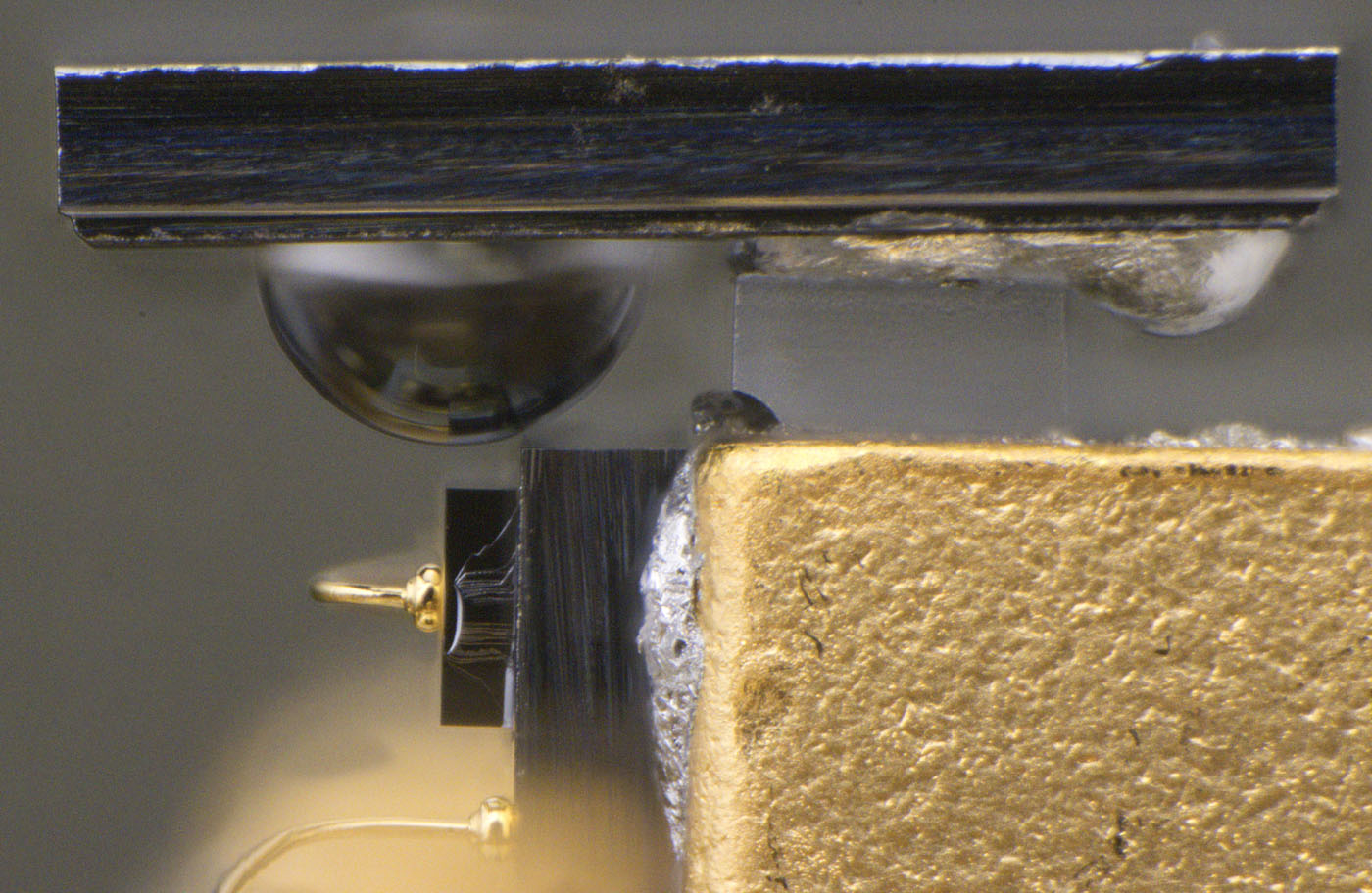
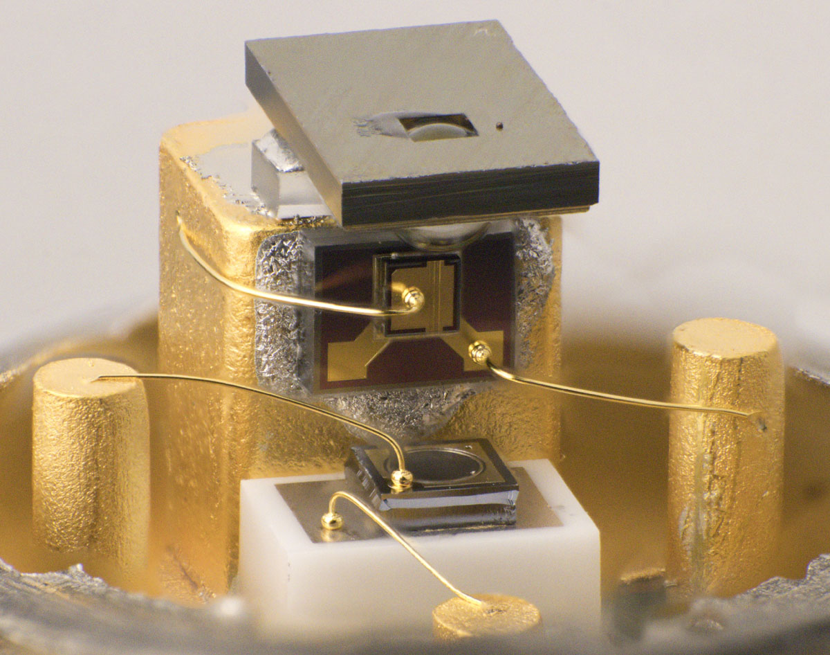
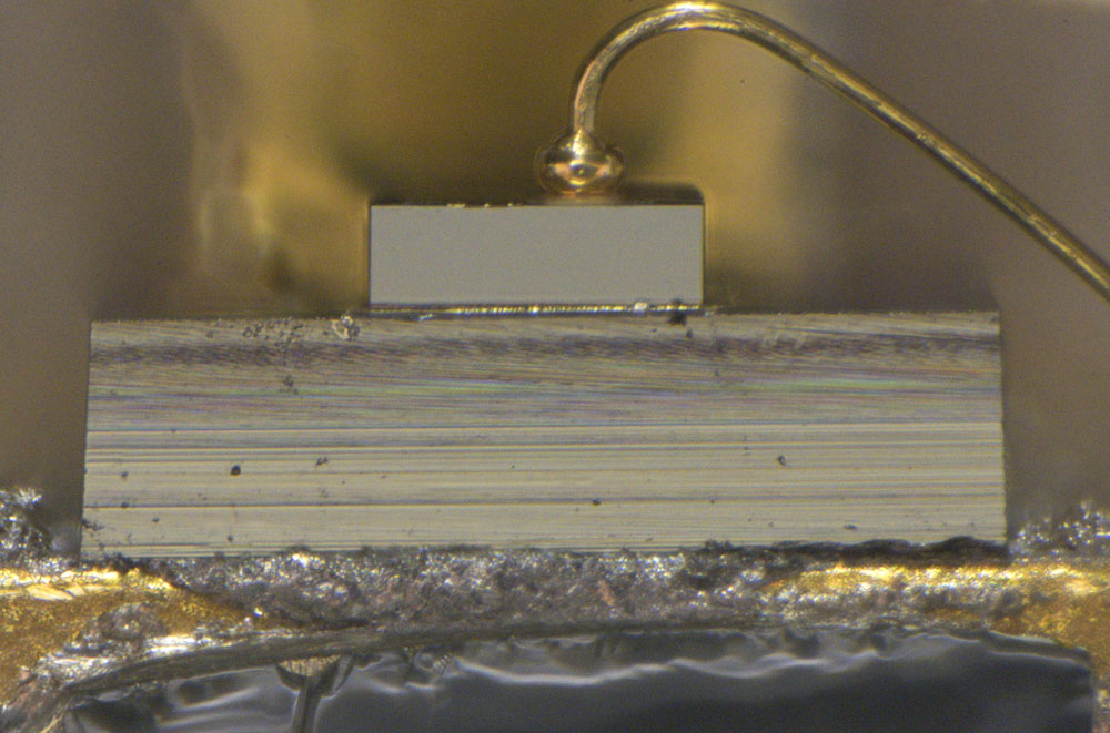
The lens carrier is attached to the protruding element of the package with a transparent block, which also carries the laser diode. The distance between the lens and the laser diode is just 30µm.
The lens has a diameter of 0,5 mm and was inserted from below into an indentation in the carrier.
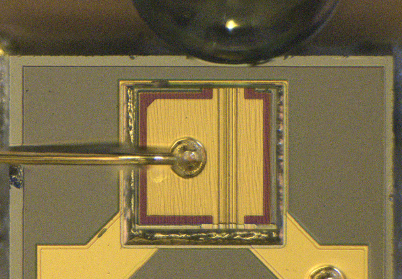
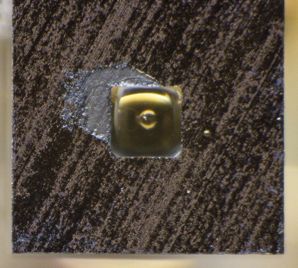
The laser diode is a typical edge emitter. It is located on a carrier and has an edge length of 0,3 mm. The laser diode in the low-cost laser module (
https://www.richis-lab.de/Opto20.htm) has a smooth surface and generates the laser beam on the underside. The laser diode shown here is more similar to the laser diodes in the Kyocera 910-00011-IT (
https://www.richis-lab.de/Opto14.htm), where the laser channel is visible on the upper side. It is a 40µm wide structure. At higher currents, as in the Kyocera module, the current is usually supplied and drained via the metal layer. In this case, the metal layer only represents one potential of the supply voltage and the circuit is closed via the substrate.
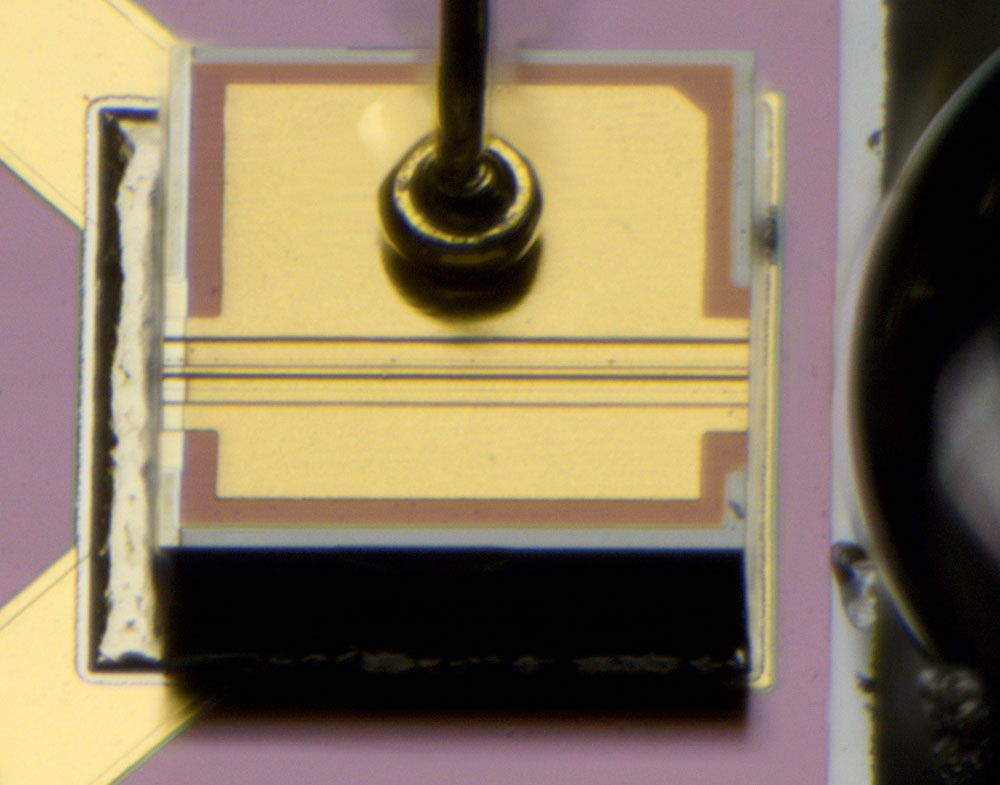
While the sides of the laser diode have broken edges, the front is polished so that the laser light can escape as efficiently as possible. This is clearly evident when compared to the surface structure of the carrier.
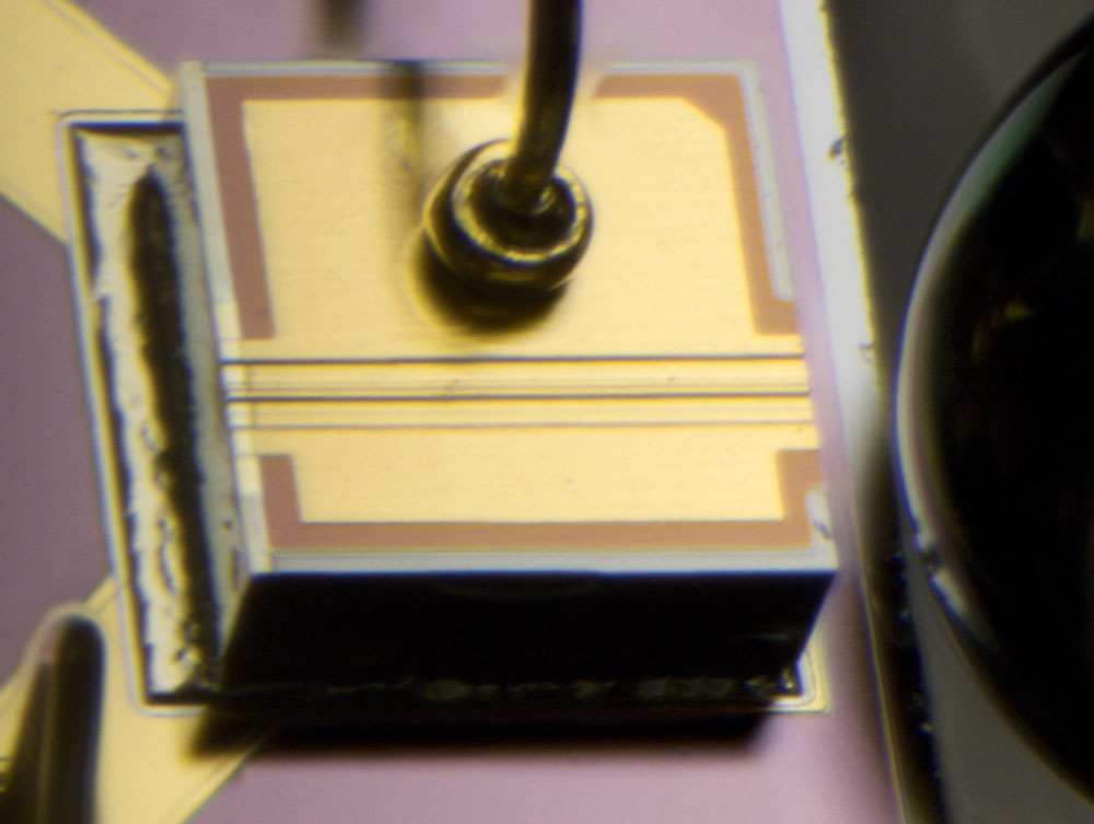
The lower side of the laser diode is difficult to image. It appears to be very smooth, which is only logical as it is the second reflective surface of the laser. In the area of the laser structures, a bright layer extends beyond the edge. It remains unclear what the purpose of this layer is.
A small part of the laser light leaves the laser diode at the rear end and hits the photodiode placed there. The current flow through the photodiode can be used to determine the current output power of the laser.
https://www.richis-lab.de/Opto25.htm 


